
This page intentionally left blank

BUILDING
SCIENTIFIC
APPARATUS
Fourth Edition
Unrivalled in its coverage and unique in its hands-on
approach, this guide to the design and construction of
scientific apparatus is essential reading for all scientists and
students in the physical, chemical, and biological sciences
and engineering.
Covering the physical principles governing the opera-
tion of the mechanical, optical and electronic parts of an
instrument, the fourth edition contains new sections on
detectors, low-temperature measurements, high-pressure
apparatus, and updated engineering specifications. There
are over 400 figures and tables to permit specification of
the components of apparatus, many new to this edition.
Data on the properties of materials and components used
by manufacturers are included. Mechanical, optical, and
electronic construction techniques carried out in the labo-
ratory, as well as those let out to specialized shops, are also
described. Step-by-step instruction, supported by many
detailed figures, is given for laboratory skills such as sol-
dering electrical components, glassblowing, brazing,
and polishing.
john h. moore is Professor Emeritus at the University of
Maryland. He is a Fellow of the American Physical Society and
the American Association for the Advancement of Science.
His research has included plasma chemistry, high-energy electron
scattering, and the design and fabrication of instruments for use in
the laboratory and on spacecraft.
christopher c. davis is Professor of Electrical and Com-
puter Engineering at the University of Maryland. He is a Fellow of
the Institute of Physics, and a Fellow of the Institute of Electrical and
Electronics Engineers. Currently his research deals with free space
optical and directional RF communication systems, plasmonics,
near-field scanning optical microscopy, chemical and biological
sensors, interferometry, optical systems, bioelectromagnetics, and
RF dosimetry.
michael a. coplan is Professor and Director of the Chem-
ical Physics Program at the University of Maryland. He is a Fellow of
the American Physical Society and has research programs in space
science, electron scattering, and neutron detection.
sandra c. greer is Professor Emerita of Chemistry and Bio-
chemistry and Professor of Chemical and Biomolecular Engineer-
ing at the University of Maryland and is now Provost and Dean of
the Faculty at Mills College in Oakland, California. She is a Fel-
low of the American Physical Society and the American Associ-
ation for the Advancement of Science, and recipient of the
American Chemical Society Francis P. Garvan–John M. Olin
Medal.
Building Scientific Apparatus covers a wide range of topics
critical to the construction, use, and understanding of sci-
entific equipment. It serves as a reference to a wealth of
technical information, but is also written in a familiar style
that makes it accessible as an introductory text. This new
edition includes updates throughout, and will continue to
serve as a bookshelf standard in laboratories around the
world. I never like to be too far from this book!
Jason Hafner, Rice University, Houston, Texas
For many years, Building Scientific Apparatus has been the
first book I reach for to remind myself of an experimental
technique, or to start learning a new one. And it has been
one of the first references I’ve recommended to new stu-
dents. With valuable additions (e.g. tolerances table for
machining, formula for aspheric lenses, expanded infor-
mation on detector signal-to-noise ratios, solid-state
detectors...) and updated lists of suppliers, the newest
addition will be a welcome replacement for our lab’s
well-thumbed previous editions of BSA.
Brian King, McMaster University, Canada
I like this book a lot. It is comprehensive in its coverage of
a wide range of topics that an experimentalist in the phys-
ical sciences may encounter. It usefully extends the scope
of previous editions and highlights new technical develop-
ments and ways to apply them. The authors share a rich
pool of knowledge and practical expertise and they have
produced a unique and authoritative guide to the building
of scientific apparatus. The book provides lucid descrip-
tions of underlying physical principles. It is also full of
hands-on advice to enable the reader to put these principles
into practice. The style of the book is very user-friendly
and the text is skillfully illustrated and informed by numer-
ous figures. The book is a mine of useful information
ranging from tables of the properties of materials to lists
of manufacturers and suppliers. This book would be an
invaluable resource in any laboratory in the physical sci-
ences and beyond.
George King, University of Manchester
The construction of novel equipment is often a prerequi-
site for cutting-edge scientific research. Jack Moore and
his coauthors have made this task easier and more effi-
cient by co ncentrating several careers’ worth of equip-
ment-building experience into a singl e volume – a
thoroughly revised and updated edition of a 25-year-old
classic. Covering areas ranging from glassblowing to
electron optics and from temperature controllers to
lasers, the invaluable information in this book is destined
to save years of collective frustration for students and
scientists. It is a ‘‘must-have’’ on the sh elf of every
research lab.
Nicholas Spencer, Eidgeno
¨
ssische Technische
Hochschule, Zu
¨
rich.
This book is a unique resource for the beginning experi-
menter, and remains valuable throughout a scientist’s
career. Professional engineers I know also own and enjoy
using the book.
Eric Zimmerman, University of Colorado at Boulder,
Colorado

BUILDING
SCIENTIFIC
APPARATUS
Fourth Edition
John H. Moore F Christopher C. Davis F Michael A. Coplan,
with
a chapter by Sandra C. Greer

CAMBRIDGE UNIVERSITY PRESS
Cambridge, New York, Melbourne, Madrid, Cape Town, Singapore,
São Paulo, Delhi, Dubai, Tokyo
Cambridge University Press
The Edinburgh Building, Cambridge CB2 8RU, UK
First published in print format
ISBN-13 978-0-521-87858-6
ISBN-13 978-0-511-58009-3
© J. Moore, C. Davis, M. Coplan, and S. Greer 2009
2009
Information on this title: www.cambrid
g
e.or
g
/9780521878586
This publication is in copyright. Subject to statutory exception and to the
provision of relevant collective licensing agreements, no reproduction of any part
may take place without the written permission of Cambridge University Press.
Cambridge University Press has no responsibility for the persistence or accuracy
of urls for external or third-party internet websites referred to in this publication,
and does not guarantee that any content on such websites is, or will remain,
accurate or appropriate.
Published in the United States of America by Cambridge University Press, New York
www.cambridge.org
eBook
(
EBL
)
Hardback
To our families

CONTENTS
Preface xiii
1
MECHANICAL DESIGN AND
FABRICATION
1
1.1 Tools and Shop Processes 2
1.1.1 Hand Tools 2
1.1.2 Machines for Making Holes 2
1.1.3 The Lathe 4
1.1.4 Milling Machines 7
1.1.5 Electrical Discharge Machining (EDM) 9
1.1.6 Grinders 9
1.1.7 Tools for Working Sheet Metal 10
1.1.8 Casting 10
1.1.9 Tolerance and Surface Quality for Shop Processes 12
1.2 Properties of Materials 12
1.2.1 Parameters to Specify Properties of Materials 13
1.2.2 Heat Treating and Cold Working 14
1.2.3 Effect of Stress Concentration 16
1.3 Materials 18
1.3.1 Iron and Steel 18
1.3.2 Nickel Alloys 20
1.3.3 Copper and Copper Alloys 21
1.3.4 Aluminum Alloys 22
1.3.5 Other Metals 22
1.3.6 Plastics 23
1.3.7 Glasses and Ceramics 24
1.4 Joining Materials 25
1.4.1 Threaded Fasteners 25
1.4.2 Rivets 28
1.4.3 Pins 29
1.4.4 Retaining Rings 29
1.4.5 Soldering 30
1.4.6 Brazing 31
1.4.7 Welding 33
1.4.8 Adhesives 34
1.4.9 Design of Joints 34
1.4.10 Joints in Piping and Pressure Vessels 37
1.5 Mechanical Drawing 39
1.5.1 Drawing Tools 39
1.5.2 Basic Principles of Mechanical Drawing 40
1.5.3 Dimensions 44
1.5.4 Tolerances 46
1.5.5 From Design to Working Drawings 48
1.6 Physical Principles of Mechanical Design 49
1.6.1 Bending of a Beam or Shaft 50
1.6.2 Twisting of a Shaft 52
1.6.3 Internal Pressure 52
1.6.4 Vibration of Beams and Shafts 54
1.6.5 Shaft Whirl and Vibration 55
1.7 Constrained Motion 57
1.7.1 Kinematic Design 57
1.7.2 Plain Bearings 59
1.7.3 Ball Bearings 60
1.7.4 Linear-Motion Bearings 61
1.7.5 Springs 62
1.7.6 Flexures 63
Cited References 66
General References 66
Chapter 1 Appendix 68
vii

2
WORKING WITH GLASS 76
2.1 Properties of Glasses 76
2.1.1 Chemical Composition and Chemical Properties of Some
Laboratory Glasses 76
2.1.2 Thermal Properties of Laboratory Glasses 77
2.1.3 Optical Properties of Laboratory Glassware 78
2.1.4 Mechanical Properties of Glass 78
2.2 Laboratory Components Available in
Glass
78
2.2.1 Tubing and Rod 78
2.2.2 Demountable Joints 79
2.2.3 Valves and Stopcocks 80
2.2.4 Graded Glass Seals and Glass-to-Metal Seals 81
2.3 Laboratory Glassblowing Skills 81
2.3.1 The Glassblower’s Tools 81
2.3.2 Cutting Glass Tubing 82
2.3.3 Pulling Points 83
2.3.4 Sealing Off a Tube: The Test-Tube End 84
2.3.5 Making a T-Seal 85
2.3.6 Making a Straight Seal 87
2.3.7 Making a Ring Seal 87
2.3.8 Bending Glass Tubing 88
2.3.9 Annealing 88
2.3.10 Sealing Glass to Metal 89
2.3.11 Grinding and Drilling Glass 91
Cited References 92
General References 92
3
VACUUM TECHNOLOGY 93
3.1 Gases 93
3.1.1 The Nature of the Residual Gases in a Vacuum
System 93
3.1.2 Gas Kinetic Theory 93
3.1.3 Surface Collisions 95
3.1.4 Bulk Behavior versus Molecular Behavior 95
3.2 Gas Flow 95
3.2.1 Parameters for Specifying Gas Flow 95
3.2.2 Network Equations 96
3.2.3 The Master Equation 96
3.2.4 Conductance Formulae 97
3.2.5 Pumpdown Time 98
3.2.6 Outgassing 98
3.3 Pressure and Flow Measurement 98
3.3.1 Mechanical Gauges 98
3.3.2 Thermal-Conductivity Gauges 100
3.3.3 Viscous-Drag Gauges 101
3.3.4 Ionization Gauges 101
3.3.5 Mass Spectrometers 103
3.3.6 Flowmeters 103
3.4 Vacuum Pumps 104
3.4.1 Mechanical Pumps 105
3.4.2 Vapor Diffusion Pumps 109
3.4.3 Entrainment Pumps 112
3.5 Vacuum Hardware 115
3.5.1 Materials 115
3.5.2 Demountable Vacuum Connections 118
3.5.3 Valves 120
3.5.4 Mechanical Motion in the Vacuum System 123
3.5.5 Traps and Baffles 124
3.5.6 Molecular Beams and Gas Jets 127
3.5.7 Electronics and Electricity in Vacuo 130
3.6 Vacuum-System Design and
Construction
131
3.6.1 Some Typical Vacuum Systems 132
3.6.2 Differential Pumping 138
3.6.3 The Construction of Metal Vacuum Apparatus 139
3.6.4 Surface Preparation 142
3.6.5 Leak Detection 143
3.6.6 Ultrahigh Vacuum 144
Cited References 145
General References 145
4
OPTICAL SYSTEMS 147
4.1 Optical Terminology 147
4.2 Characterization and Analysis of Optical
Systems
150
4.2.1 Simple Reflection and Refraction Analysis 150
4.2.2 Paraxial-Ray Analysis 151
4.2.3 Nonimaging Light Collectors 162
4.2.4 Imaging Systems 162
4.2.5 Exact Ray Tracing and Aberrations 166
4.2.6 The Use of Impedances in Optics 174
4.2.7 Gaussian Beams 179
viii CONTENTS

4.3 Optical Components 182
4.3.1 Mirrors 182
4.3.2 Windows 187
4.3.3 Lenses and Lens Systems 187
4.3.4 Prisms 196
4.3.5 Diffraction Gratings 201
4.3.6 Polarizers 204
4.3.7 Optical Isolators 211
4.3.8 Filters 212
4.3.9 Fiber Optics 217
4.3.10 Precision Mechanical Movement Systems 219
4.3.11 Devices for Positional and Orientational Adjustment
of Optical Components 222
4.3.12 Optical Tables and Vibration Isolation 229
4.3.13 Alignment of Optical Systems 229
4.3.14 Mounting Optical Components 230
4.3.15 Cleaning Optical Components 232
4.4 Optical Materials 236
4.4.1 Materials for Windows, Lenses, and Prisms 236
4.4.2 Materials for Mirrors and Diffraction Gratings 245
4.5 Optical Sources 247
4.5.1 Coherence 248
4.5.2 Radiometry: Units and Definitions 248
4.5.3 Photometry 249
4.5.4 Line Sources 250
4.5.5 Continuum Sources 252
4.6 Lasers 261
4.6.1 General Principles of Laser Operation 267
4.6.2 General Features of Laser Design 268
4.6.3 Specific Laser Systems 270
4.6.4 Laser Radiation 283
4.6.5 Coupling Light from a Source to an Aperture 284
4.6.6 Optical Modulators 287
4.6.7 How to Work Safely with Light Sources 289
4.7 Optical Dispersing Instruments 291
4.7.1 Comparison of Prism and Grating Spectrometers 293
4.7.2 Design of Spectrometers and Spectrographs 295
4.7.3 Calibration of Spectrometers and Spectrographs 299
4.7.4 Fabry–Perot Interferometers and Etalons 299
4.7.5 Design Considerations for Fabry–Perot Systems 308
4.7.6 Double-Beam Interferometers 309
Endnotes 314
Cited References 314
General References 318
5
CHARGED-PARTICLE OPTICS 324
5.1 Basic Concepts of Charged-Particle
Optics
324
5.1.1 Brightness 324
5.1.2 Snell’s Law 325
5.1.3 The Helmholtz–Lagrange Law 325
5.1.4 Vignetting 326
5.2 Electrostatic Lenses 327
5.2.1 Geometrical Optics of Thick
Lenses 327
5.2.2 Cylinder Lenses 329
5.2.3 Aperture Lenses 331
5.2.4 Matrix Methods 332
5.2.5 Aberrations 333
5.2.6 Lens Design Example 336
5.2.7 Computer Simulations 338
5.3 Charged-Particle Sources 338
5.3.1 Electron Guns 338
5.3.2 Electron-Gun Design
Example 341
5.3.3 Ion Sources 343
5.4 Energy Analyzers 345
5.4.1 Parallel-Plate Analyzers 346
5.4.2 Cylindrical Analyzers 347
5.4.3 Spherical Analyzers 348
5.4.4 Preretardation 350
5.4.5 The Energy-Add Lens 350
5.4.6 Fringing-Field Correction 352
5.4.7 Magnetic Energy Analyzers 353
5.5 Mass Analyzers 354
5.5.1 Magnetic Sector Mass
Analyzers 354
5.5.2 Wien Filter 354
5.5.3 Dynamic Mass Spectrometers 355
5.6 Electron- and Ion-Beam Devices:
Construction
355
5.6.1 Vacuum Requirements 355
5.6.2 Materials 356
5.6.3 Lens and Lens-Mount Design 357
5.6.4 Charged-Particle Detection 358
5.6.5 Magnetic-Field Control 358
Cited References 360
CONTENTS ix

6
ELECTRONICS 362
6.1 Preliminaries 362
6.1.1 Circuit Theory 362
6.1.2 Circuit Analysis 365
6.1.3 High-Pass and Low-Pass Circuits 369
6.1.4 Resonant Circuits 372
6.1.5 The Laplace-Transform Method 374
6.1.6 RLC Circuits 377
6.1.7 Transient Response of Resonant Circuits 378
6.1.8 Transformers and Mutual Inductance 379
6.1.9 Compensation 380
6.1.10 Filters 380
6.1.11 Computer-Aided Circuit Analysis 381
6.2 Passive Components 382
6.2.1 Fixed Resistors and Capacitors 383
6.2.2 Variable Resistors 384
6.2.3 Transmission Lines
6.2.4 Coaxial Connectors
6.2.5 Relays
6.3 Active Components 402
6.3.1 Diodes 403
6.3.2 Transistors 406
6.3.3 Silicon-Controlled Rectifiers 419
6.3.4 Unijunction Transistors 420
6.3.5 Thyratrons 421
6.4 Amplifiers and Pulse Electronics 421
6.4.1 Definition of Terms 421
6.4.2 General Transistor-Amplifier Operating
Principles 424
6.4.3 Operational-Amplifier Circuit Analysis 428
6.4.4 Instrumentation and Isolation Amplifiers 432
6.4.5 Stability and Oscillators 434
6.4.6 Detecting and Processing Pulses 435
6.5 Power Supplies 441
6.5.1 Power-Supply Specifications 442
6.5.2 Regulator Circuits and Programmable Power
Supplies 443
6.5.3 Bridges 445
6.6 Digital Electronics 447
6.6.1 Binary Counting 447
6.6.2 Elementary Functions 447
6.6.3 Boolean Algebra 448
6.6.4 Arithmetic Units 448
6.6.5 Data Units 448
6.6.6 Dynamic Systems 450
6.6.7 Digital-to-Analog Conversion 453
6.6.8 Memories 458
6.6.9 Logic and Function 460
6.6.10 Implementing Logic Functions 464
6.7 Data Acquisition 467
6.7.1 Data Rates 467
6.7.2 Voltage Levels and Timing 469
6.7.3 Format 469
6.7.4 System Overhead 470
6.7.5 Analog Input Signals 472
6.7.6 Multiple Signal Sources: Data Loggers 474
6.7.7 Standardized Data-Acquisition Systems 474
6.7.8 Control Systems 479
6.7.9 Personal Computer (PC) Control of Experiments 482
6.8 Extraction of Signal from Noise 491
6.8.1 Signal-to-Noise Ratio 491
6.8.2 Optimizing the Signal-to-Noise Ratio 492
6.8.3 The Lock-In Amplifier and Gated Integrator or
Boxcar 493
6.8.4 Signal Averaging 494
6.8.5 Waveform Recovery 495
6.8.6 Coincidence and Time-Correlation Techniques 496
6.9 Grounds and Grounding 500
6.9.1 Electrical Grounds and Safety 500
6.9.2 Electrical Pickup: Capacitive Effects 503
6.9.3 Electrical Pickup: Inductive Effects 504
6.9.4 Electromagnetic Interference and r.f.i 505
6.9.5 Power-Line-Coupled Noise 505
6.9.6 Ground Loops 506
6.10 Hardware and Construction 508
6.10.1 Circuit Diagrams 508
6.10.2 Component Selection and Construction Techniques 508
6.10.3 Printed Circuit Boards 513
6.10.4 Wire Wrapä Boards 523
6.10.5 Wires and Cables 524
6.10.6 Connectors 528
6.11 Troubleshooting
6.11.1 General Procedures
6.11.2 Identifying Parts 535
Cited References 537
General References 538
Chapter 6 Appendix 541
x CONTENTS
388
399
401
533
533

7
DETECTORS 547
7.1 Optical Detectors 547
7.2 Noise in Optical Detection Process 548
7.2.1 Shot Noise 548
7.2.2 Johnson Noise 549
7.2.3 Generation-Recombination (gr) Noise 549
7.2.4 1/f Noise 549
7.3 Figures of Merit for Detectors 550
7.3.1 Noise-Equivalent Power 550
7.3.2 Detectivity 550
7.3.3 Responsivity 551
7.3.4 Quantum Efficiency 552
7.3.5 Frequency Response and Time Constant 553
7.3.6 Signal-to-Noise Ratio 553
7.4 Photoemissive Detectors 554
7.4.1 Vacuum Photodiodes 554
7.4.2 Photomultipliers 555
7.4.3 Photocathode and Dynode Materials 556
7.4.4 Practical Operating Considerations for Photomultiplier
Tubes 561
7.5 Photoconductive Detectors 566
7.6 Photovoltaic Detectors
(Photodiodes)
572
7.6.1 Avalanche Photodiodes 574
7.6.2 Geiger Mode Avalanche Photodetectors 577
7.7 Detector Arrays 578
7.7.1 Reticons 578
7.7.2 Quadrant Detectors 578
7.7.3 Lateral Effect Photodetectors 578
7.7.4 Imaging Arrays 580
7.7.5 Image Intensifiers 581
7.8 Signal-to-Noise Ratio Calculations 582
7.8.1 Photomultipliers 582
7.8.2 Direct Detection with p–i–n Photodiodes 582
7.8.3 Direct Detection with APDs 584
7.8.4 Photon Counting 585
7.9 Particle and Ionizing Radiation
Detectors
585
7.9.1 Solid-State Detectors 589
7.9.2 Scintillation Counters 591
7.9.3 X-Ray Detectors 591
7.10 Thermal Detectors 591
7.10.1 Thermopiles 593
7.10.2 Pyroelectric Detectors 593
7.10.3 Bolometers 594
7.10.4 The Golay Cell 595
7.11 Electronics to be Used With Detectors 596
7.12 Detector Calibration 597
Endnotes 597
Cited References 597
General References 599
8
MEASUREMENT AND CONTROL OF
TEMPERATURE
600
8.1 The Measurement of Temperature 600
8.1.1 Expansion Thermometers 601
8.1.2 Thermocouples 602
8.1.3 Resistance Thermometers 605
8.1.4 Semiconductor Thermometers 609
8.1.5 Temperatures Very Low: Cryogenic
Thermometry 610
8.1.6 Temperatures Very High 611
8.1.7 New, Evolving, and Specialized Thermometry 612
8.1.8 Comparison of Main Categories of
Thermometers 612
8.1.9 Thermometer Calibration 612
8.2 The Control of Temperature 613
8.2.1 Temperature Control at Fixed Temperatures 613
8.2.2 Temperature Control at Variable Temperatures 613
Cited References 621
General References 623
Index 625
CONTENTS xi

PREFACE
Building Scientific Apparatus provides an overview of the
physical principles that one must grasp to make useful and
creative decisions in the design of scientific apparatus. We
also describe skills, such as mechanical drawing, circuit
analysis, and optical ray-tracing and matrix methods
that are required to design an instrument. A large part
of the text is devoted to components. For each class of
components – electrical, optical, thermal and so on – the
parameters used by manufacturers to specify their products
are defined. Useful materials and components such as
infrared detectors, metal alloys, optical materials, and
operational amplifiers are discussed, and examples and
performance specifications are given. Of course, having
designed an apparatus and chosen the necessary compo-
nents, one must build it. We deal in considerable detail
with basic laboratory skills: soldering electrical compo-
nents, glassblowing, brazing, polishing, and so on.
Described in lesser detail are operations such as lathe turn-
ing, milling, casting, laser cutting, and printed-circuit pro-
duction, which one might let out to an outside shop.
Understanding the capabilities and limitations of shop pro-
cesses is necessary to fully exploit them in designing and
building an instrument. Overall, we recognize that there
are many engineering and technical texts that cover every
aspect of instrument design; our goal in Building Scientific
Apparatus has been to winnow the available information
down to the essentials required for practical work by the
designer and builder of scientific instruments.
In the 25 years since Building Scientific Apparatus first
appeared, there have been profound changes in the way in
which unique apparatus is assembled, as well as in the
scientists who require unique apparatus. Twenty-five years
ago the technology discussed in the first edition – optics,
electronics, charged-particle beams, and vacuum systems –
was generally the purview of engineers. Today sophisti-
cated apparatus is conceived of and built by chemists,
physicists, and biologists, as well as medical and social
scientists. In the past, microprocessors were a component
that needed to be programmed and wired into an apparatus.
Now computer controls are an integral part of devices such
as power supplies, pressure gauges, and machine tools.
Similarly, lasers were once assembled in the lab from indi-
vidual optical components; today a complete laser is itself
a component, less expensive than the elements from which
it is assembled. The fourth edition of Building Scientific
Apparatus recognizes this evolution in the complexity of
available components and the concomitant implications
for the instrument designer.
We acknowledge the importance that the World Wide
Web has acquired as a resource for research. Throughout
the text we mention particular suppliers of materials and
components. There are certainly many that have escaped
our attention. The suppliers of equipment, devices, com-
ponents, and materials along with specifications, availabil-
ity, and cost can be readily located using a suitable search
engine.
This book was written with the goal of contributing to
the quality and functionality of apparatus designed and
built for research in disciplines from the engineering and
physical sciences to the life sciences. We welcome com-
ments; many suggestions from the past have been incorpo-
rated in the current text.
xiii

MECHANICAL DESIGN AND FABRICATION
Every scientific apparatus requires a mechanical structure,
even a device that is fundamentally electronic or optical in
nature. The design of this structure determines to a large
extent the usefulness of the apparatus. It follows that a
successful scientist must acquire many of the skills of
the mechanical engineer in order to proceed rapidly with
an experimental investigation.
The designer of research apparatus must strike a balance
between the makeshift and the permanent. Too little initial
consideration of the expected performance of a machine
may frustrate all attempts to get data. Too much time spent
planning can also be an error, since the performance of a
research apparatus is not entirely predictable. A new
machine must be built and operated before all the short-
comings in its design are apparent.
The function of a machine should be specified in some
detail before design work begins. One must be realistic in
specifying the job of a particular device. The introduction
of too much flexibility can hamper a machine in the per-
formance of its primary function. On the other hand, it may
be useful to allow space in an initial design for anticipated
modifications. Problems of assembly and disassembly
should be considered at the outset, since research equip-
ment rarely functions properly at first and often must be
taken apart and reassembled repeatedly.
Make a habit of studying the design and operation of
machines. Learn to visualize in three dimensions the size
and positions of the parts of an instrument in relation to
one another.
Before beginning a design, learn what has been done
before. It is a good idea to build and maintain a library
of commercial catalogs in order to be familiar with what is
available from outside sources. Too many scientific
designers waste time and money on the reinvention of
the wheel and the screw. Use nonstandard parts only when
their advantages justify the great cost of one-off con-
struction in comparison with mass production. Consider
modifications of a design that will permit the use of stand-
ardized parts. An evening spent leafing through the catalog
of one of the major tool and hardware suppliers can be
remarkably educational – catalogs from McMaster-Carr
or W. M. Berg, for example, each list over 200 000 stand-
ard fasteners, bearings, gears, mechanical and electrical
parts, tools etc.
Become aware of the available range of commercial
services. In most big cities, specialty job shops perform
such operations as casting, plating, and heat-treating inex-
pensively. In many cases it is cheaper to have others pro-
vide these services rather than attempt them oneself. Some
of the thousands of suppliers of useful services, as well as
manufacturers of useful materials, are noted throughout
the text.
In the following sections we discuss the properties of
materials and the means of joining materials to create a
machine. The physical principles of mechanical design are
presented. These deal primarily with controlling the
motion of one part of a machine with respect to another,
both where motion is desirable and where it is not. There
are also sections on machine tools and on mechanical
drawing. The former is mainly intended to provide enough
information to enable the scientist to make intelligent use
of the services of a machine shop. The latter is presented in
sufficient detail to allow effective communication with
people in the shop.
1
CHAPTER
1

1.1 TOOLS AND SHOP PROCESSES
A scientist must be able to make proper use of hand tools to
assemble and modify research apparatus. A successful
experimentalist should be able to perform elementary
operations safely with a drill press, lathe, and milling
machine in order to make or modify simple components.
Even when a scientist works with instruments that are
fabricated and maintained by research technicians and
machinists, an elementary knowledge of machine-tool
operations will allow the design of apparatus that can
be constructed with efficiency and at reasonable cost.
The following is intended to familiarize the reader with
the capabilities of various tools. Skill with machine tools
is best acquired under the supervision of a competent
machinist.
1.1.1 Hand Tools
A selection of hand tools for the laboratory is given in
Table 1.1. A research scientist in physics or chemistry will
hav
e use for most of these tools, and if possible should
have the entire set in the lab. The tool set outlined in Table
1.1 is not too expensive for any scientist to have on hand.
A
laboratory scientist should adopt a craftsman-like atti-
tude toward tools. Far less time is required to find and use
the proper tool for a job than will be required to repair the
damage resulting from using the wrong one.
1.1.2 Machines for Making Holes
Holes up to about 25 mm (1 in.) diameter are made using
a twist drill (Figure 1.1) in a drill press. A boring
bar
Table 1.1 Tool Set for Laboratory Use
Screwdrivers:
No. 1, 2, and 3 drivers for slotted-head screws
No. 1, 2, and 3 Phillips screwdrivers
Allen (hex) drivers for socket-head screws, both a
fractional set (1/16–1/4 in.) and a metric set (1.5–10 mm)
Nut drivers for hex-head screws and nuts, both fractional
(1/8–1/2 in.) and metric (4–11 mm)
Set of jeweller’s screwdrivers
Wrenches:
Combination box and open-end wrenches, both a
fractional set (3/8–1 in.) and a metric set (10–19 mm)
3/8 in. square-drive ratcheting socket driver with both
fractional (3/8–7/8 in.) and metric (10–19 mm) socket sets
Adjustable wrenches (small, medium, and large)
Pipe wrench
Pliers:
Slip-joint pliers
Channel-locking pliers
Large and small needle-nose pliers
Large and small diagonal cutters
Small flush cutters
Hemostats
Hammers:
Small and medium ball-peen hammers
Soft-faced hammer with plastic or rubber inserts
Files:
Second-cut, flat, half-round, and round files with handles
Smooth-cut, flat, half-round, and round files with handles
Six-piece Swiss-Pattern file set
Miscellaneous:
Dial caliper or micrometer
Forceps
Sheet-metal shears
Hacksaw
Tubing cutter
Center punch
Scriber
Small machinist’s square
Steel scale
Divider
Tapered hand reamer
Tap wrench with:
4-40 to 1/4-20 UNC and 3 3 0.6 to 12 3 1.75 metric
tap sets
1/8 to 1/2 NPT or 6 mm to 15 mm BPST (metric) pipe
thread tap sets
Electric hand drill motor or small drill press
Drills, 1/16–1/2 in. in 1/32 in. increments, in drill index
Drills, Nos. 1–60, in drill index
Small bench vise
2 MECHANICAL DESIGN AND FABRICATION
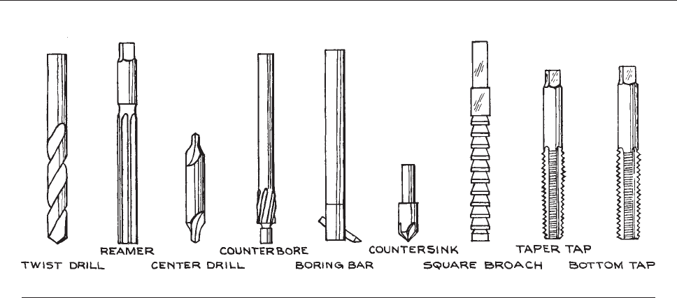
(Figure 1.1) is used in a lathe or vertical milling machine to
bore out a drilled hole to make a large hole. Of course,
a hole can be drilled with a twist drill in a handheld
drill motor; this method, although convenient, is not very
accurate and should only be employed when it is not pos-
sible to mount the work on the drill press table.
Twist drills are available in fractional inch sizes and
metric sizes as well as in number and letter series of sizes
at intervals of only a few thousandths of an inch. Sizes
designated by common fractions are available in 1/64 in.
increments in diameters from 1/64 to 1 3/4 in., in 1/32 in.
increments in diameters from 1 3/4 to 2 1/4 in., and in
1/16 in. increments in diameters from 2 1/4 to 3 1/2 in;
metric sizes are available in 0.05 mm increments in diam-
eters from 1.00 mm to 2.50 mm, in 0.10 mm increments
from 2.50 mm to 10.00 mm, and in 0.50 mm increments
from 10.00 mm to 17.50 mm. Number drill sizes are given
in Appendix 1.1. The included angle at the point of a drill
is
118°. A designer should always choose a hole size that
can be drilled with a standard-size drill, and the shape of the
bottom of a blind hole should be taken to be that left by a
standard drill unless another shape is absolutely necessary.
If many holes of the same size are to be drilled, it may be
worthwhile to alter the drill point to provide the best per-
formance in the material that is being drilled. In very hard
materials the included angle of the point should be increased
to as much as 140°. For soft materials such as plastic or fiber
it should be decreased to about 90°. Many shops maintain a
set of drills with points specially ground for drilling in brass.
The included angle of such a drill is 118°, but the cutting
edge is ground so that its face is parallel to the axis of the
drill in order to prevent the drill from digging in.
A drilled hole can be located to within about 0.3 mm
(0.01 in.) by scribing two intersecting lines and making a
punch mark at the intersection. The indentation made by
the punch holds the drill point in place until the cutting
edges first engage the material to be drilled. With care,
locational accuracy of 0.03 mm (.001 in.) can be achieved
in a milling machine or jig borer. Locational error is pri-
marily a result of the drill’s flexing as it first enters the
material being drilled. This causes the point of the drill to
wander off the center of rotation of the machine driving the
drill; the hole should be started with a center drill (Figure
1.1) that is short and stiff. Once the hole is started, drilling
is
completed with the chosen twist drill.
A drill tends to produce a hole that is out-of-round and
oversize by as much as 0.2 mm (.005 in.). Also, a drill
point tends to deviate from a straight line as it moves
through the material being drilled. This run-out can
amount to 0.2 mm (.008 in.) for a 6 mm (1/4 in.) drill
making a 25 mm (1 in.) deep hole; more for a smaller
diameter drill. It is particularly difficult to make a round
hole when drilling material that is so thin that the drill
point breaks out on the under side before the shoulder
Figure 1.1 Tools for making and shaping holes.
TOOLS AND SHOP PROCESSES 3

enters the upper side. Clamping the work to a backup block
of similar material alleviates the problem. When roundness
and diameter tolerances are important, it is good practice
to drill a hole slightly undersize and finish up with the
correct size drill; better yet, the undersized hole can be
accurately sized using a reamer.
Before drilling in a drill press, the location of the hole
should be center-punched and the work should be securely
clamped to the drill-press table. The drill should enter
perpendicular to the work surface. When drilling curved
or canted surfaces, it is best to mill a flat, perpendicular to
the hole axis at the location of the hole.
The speed at which the drill turns is determined by the
maximum allowable surface speed at the outer edge of the bit
as well as the rate at which the drill is fed into the work. The
rate at which a tool cuts is typically specified as meters per
minute (m/min) or surface feet per minute (sfpm). Suggested
tool speeds are given in Table 1.2. A drill (or any cutting
tool)
should be cooled and lubricated by flooding with solu-
ble cutting oil, kerosene, or other cutting fluid. Brass or
aluminum can be drilled without cutting oil if necessary.
A drilled hole that must be round and straight to close tol-
erances is drilled slightly undersize and then reamed using a
tool such as is shown in Figure 1.1.Reamerswitharound
sh
ank are meant to be grasped in the collet chuck of a mill-
ing machine; the reamer inserted after the drill is removed
from the chuck without moving the work-piece on the bed of
the milling machine. A reamer with a square shank is to be
grasped in a tap handle for use by hand. A hand reamer has a
slight initial taper to facilitate starting the cut. The diameter
tolerance on a reamed hole can be 0.03 mm (.001 in.) or
better. The chamfer (taper) tolerance can be kept to 0.0002
millimeter per millimeter (or 8 microinch per inch) or better.
Tapered drill and reamer sets are available for preparing the
tapered holes for standard taper pins used to secure one part
to another with great and repeatable precision.
A drilled hole can be threaded with a tap (shown in
Figure 1.1). Cutting threads with a tap is usually carried
out
by hand. A tap has a square shank that is clamped in a
tap handle. The tap is inserted in the hole and slowly turned,
cutting as it goes. The tool should be lubricated and should
be backed at least part way out of the hole after each full
turn of cutting in order to clear metal chips from the tool.
Taps are chamfered (tapered) on the end so that the first few
teeth do not cut full depth. This makes for smoother cutting
and better alignment. For more precise tapping the tap can
be placed in a drill press with the work-piece held under-
neath. The drill chuck can be rotated by hand to start the tap
off correctly, parallel to the hole. Some drill presses come
with a foot-operated reversing mechanism so that with the
drill operating at a slow speed the correct action of tap–
reverse-tap can be carried out. The chamfer on a tap extends
for nearly 10 teeth in a taper tap, 3 to 5 teeth on a plug tap,
and 1 to 2 teeth on a bottom tap. The first two are intended
for threading through a hole, the latter for finishing the
threads in a blind hole. The hole to be threaded is drilled
with a tap drill with a diameter specified to allow the tap to
cut threads to about 75% of full depth. Appendix 1.1 gives
ta
p drill sizes for American National and metric threads.
The head of a bolt can be recessed by enlarging the entra-
nce of the bolt hole with a counterbore (shown in Figure 1.1).
A
keyway slot can be added to a drilled hole or a drilled
hole can be made square or hexagonal by shaping the hole
with a broach (Figure 1.1). A broach is a cutting tool with a
series
of teeth of the desired shape, each successive cutting
edge slightly larger than the one preceding. The broach can
be driven through the hole by a hand-driven or hydraulic
press. In some broaching machines the tool is pulled
through the work. A broach can, at some expense, be
ground to a nonstandard shape. The expense is probably
only justified if many holes are to be broached.
1.1.3 The Lathe
A lathe (Figure 1.2) is used to produce a surface of revo-
lution such as a cylindrical or conical surface. The work to
Table 1.2 Tool Speeds for High-speed Steel Tools
(Speeds can be increased 2 3 with carbide-tipped tools)
Material m/min (sfpm)
Drill Lathe Mill
Aluminum 60 (200) 100 (300) 120 (400)
Brass 60 (200) 50 (150) 60 (200)
Cast iron 30 (100) 15 (50) 15 (50)
Carbon steel 25 (80) 30 (100) 20 (60)
Stainless steel 10 (30) 30 (100) 20 (60)
Copper 60 (200) 100 (300) 30 (100)
Plastics 30 (100) 60 (200) 60 (200)
4 MECHANICAL DESIGN AND FABRICATION
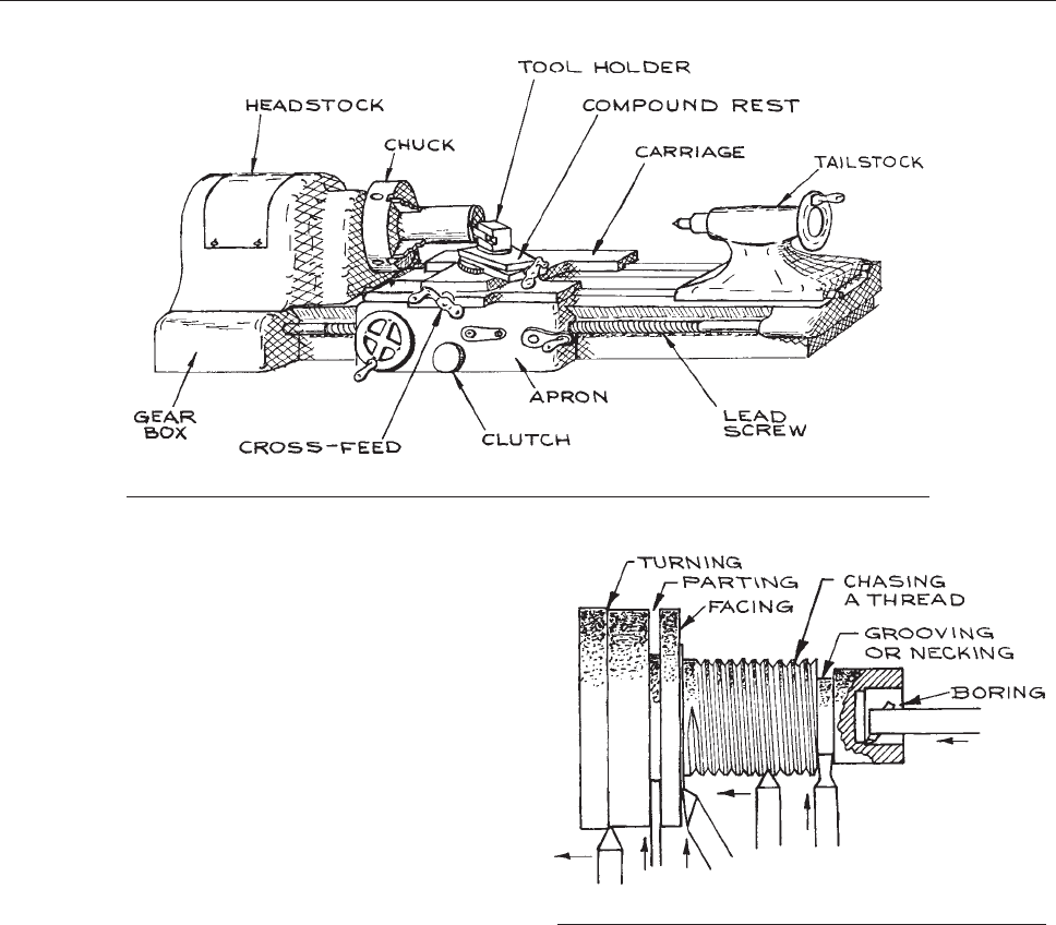
be turned is grasped by a chuck that is rotated by the driv-
ing mechanism within the lathe headstock. Long pieces are
supported at the free end by a center mounted in the tail-
stock. A cutting tool held atop the lathe carriage is brought
against the work as it turns. As shown in Figure 1.2, the
tool
holder is clamped to the compound rest mounted to a
rotatable table atop the cross-feed that in turn rests on the
carriage. The carriage can be moved parallel to the axis of
rotation along slides or ways on the lathe bed. A cylindri-
cal surface is produced by moving the carriage up or down
the ways, as in the first cut illustrated in Figure 1.3. Driving
the
cross-feed produces a face perpendicular to the axis of
rotation; driving the tool with the compound-rest screw
produces a conical surface.
Most lathes have a lead screw along the side of the lathe
bed. This screw is driven in synchronization with the rotat-
ing chuck by the motor drive of the lathe. A groove running
the length of the lead screw can be engaged by a clutch in
the carriage apron to provide power to drive either the
carriage or the cross-feed in order to produce a long uni-
form cut. When cutting threads the lead screw can be
engaged by a split nut in the apron to provide uniform
motion of the carriage.
A variety of attachments are available for securing work
to the spindle in the headstock. Most convenient is the
three-jaw chuck. All three jaws are moved inward and
outward by a single control so that a cylinder placed in
the chuck is automatically centered. A four-jaw chuck with
independently controlled jaws is used to grasp a work-
piece that is not cylindrical or to hold a cylindrical piece
off center. Large irregular work can be bolted to a face
plate that is attached to the lathe spindle. Small round
pieces can be grasped in a collet chuck. A collet is a slotted
tube with an inner diameter of the same size as the work
and a slightly tapered outer surface. The work is clamped
Figure 1.2 A lathe.
Figure 1.3 Cuts made on a lathe.
TOOLS AND SHOP PROCESSES 5
in the collet by a mechanism that draws the collet into a
sleeve mounted in the lathe spindle.
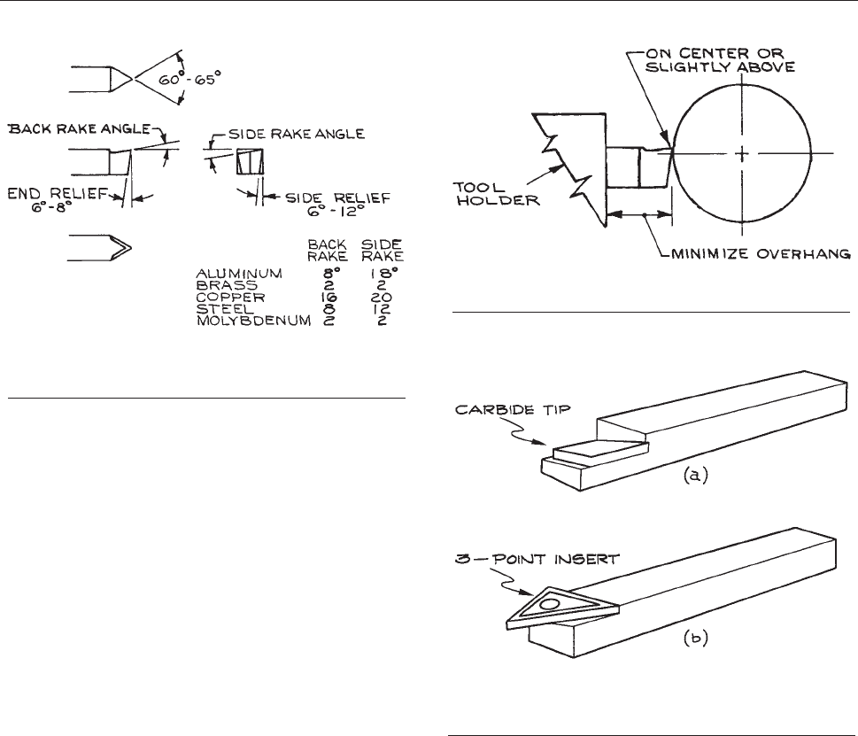
The cutting tool largely determines the quality of work
produced in a lathe. The efficiency of the tool bit used in a
lathe depends upon the shape of the cutting edge and the
placement of the tool with respect to the work-piece. A
cutting tool must be shaped to provide a good compromise
between sharpness and strength. The sharpness of the cut-
ting edge is determined by the rake angles indicated in
Figure 1.4. The indicated r
elief angles are required to pre-
vent the noncutting edges and surfaces of the tool from
interfering with the work. Placement of the tool in relation
to the work-piece is illustrated in Figure 1.5.
In
the past, a machinist was obliged to grind tool steel
stock to the required shape to made a tool bit. Now vir-
tually all work is done with prepared tool bits. These may
be simply ground-to-shape tool bits. Especially sharp,
robust tools are available with sintered tungsten carbide
(so-called ‘‘carbide’’) or diamond tips. Many tools are
made with replaceable carbide inserts. The insert, which
is clamped to the end of the tool, is triangular or square to
provide three or four cutting edges by rotating the insert in
its holder. Examples are illustrated in Figure 1.6.
As
in drilling, the cutting speed for turning in a lathe
depends upon the material being machined. Cutting speeds
for high-speed steel tools are given in Table 1.2. Modern
carbide-
and ceramic-tipped cutters are much faster than
tool-steel bits; they also produce a cleaner, more precise cut.
Typically, a cut should be 0.1 to 0.3 mm (.003–.010 in.)
deep, although much deeper cuts are permissible for rough
work if the lathe and work-piece can withstand the stress.
Holes in the center of a work-piece may be drilled by
placing a twist drill in the tailstock and driving the drill
into the rotating work with the hand-wheel drive of the
tailstock. The hole should first be located with a center
drill (Figure 1.1), or the drill point will wander off center.
Figure 1.4 Tool angles for a right-cutting round-nose tool.
A right-cutting tool has its cutting edge on the right when
viewed from the point end.
Figure 1.5 Placement of tool with respect to the work in a
lathe.
Figure 1.6 (a) Single-point carbide-tipped lathe tool.
(b) Lathe tool with replaceable carbide insert. The insert has
three cutting points.
6 MECHANICAL DESIGN AND FABRICATION
A drill, a lathe tool, or a milling cutter is usually bathed
with a cutting fluid to cool the tool and to produce a
smooth cut. Cutting fluids include soluble oils, mineral
oils, and base oils. Soluble oils form emulsions when
mixed with water and are used for cutting both ferrous
and nonferrous metals, when cooling is most important.
Mineral oils are petroleum products including paraffin oils
and kerosene. They are typically used for light, high-speed
cutting. Base oils are inorganic or fatty oils with or without
sulfur-containing additives. Base oils are called for when
making heavy cuts in ferrous materials.
Tolerances of 0.1 mm (.004 in.) can be maintained with
ease when machining parts in a lathe. Diameters accurate
to 60.01 mm (6.0004 in.) can be obtained by a skilled
operator at the expense of considerable time. Any modern
lathe will maintain a straightness tolerance of 0.4 mm/m
(0.005 in/ft) provided the work-piece is stiff enough not to
spring away from the cutting tool.
1.1.4 Milling Machines
Milling, as a machine-tool operation, is the converse of
lathe turning. In milling the work-piece is brought into
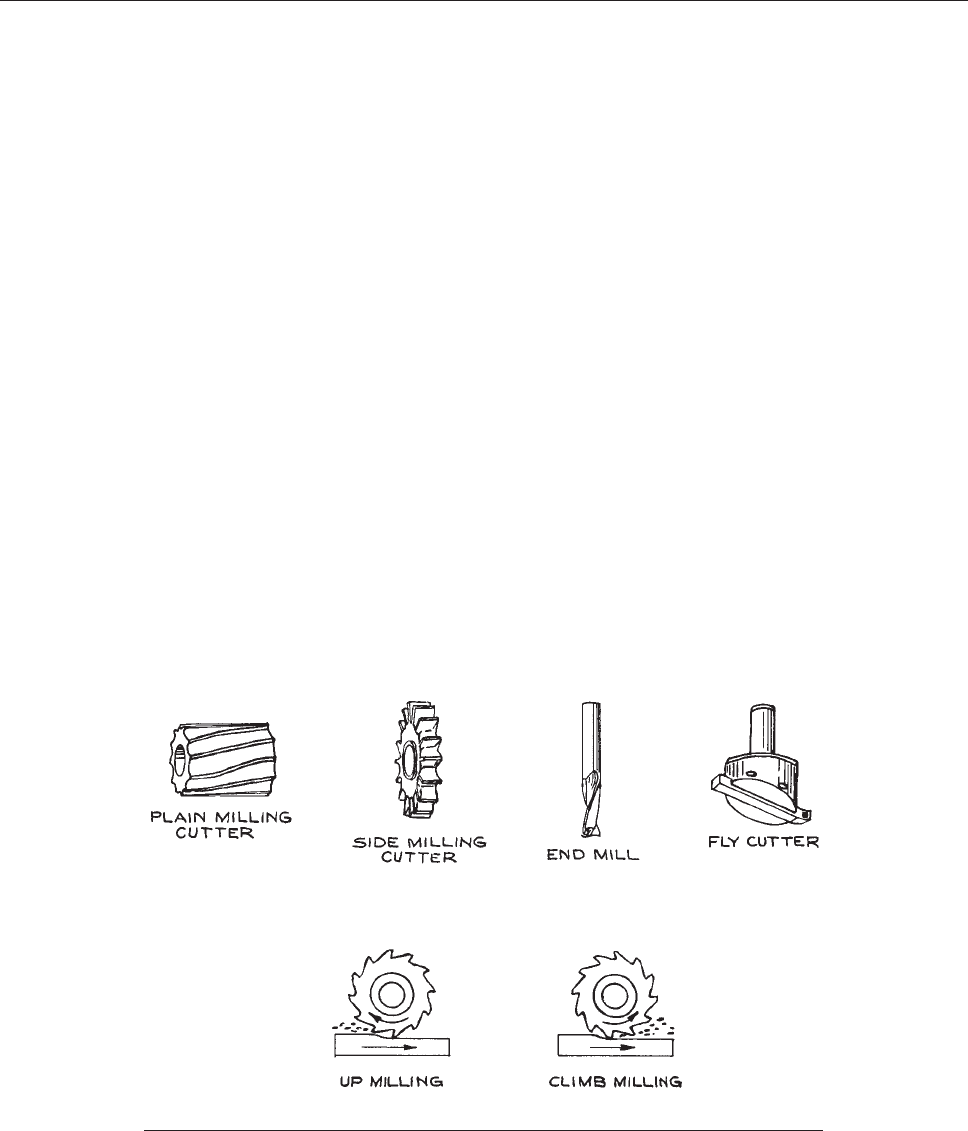
contact with a rotating cutter. Typical milling cutters are
illustrated in Figure 1.7.Aplain
milling cutter has teeth
only on the periphery and is used for milling flat surfaces.
A side milling cutter has cutting edges on the periphery
and either one or both ends so that it can be used to mill a
channel or groove. An end mill is rotated about its long
axis and has cutters on both the end and sides. There are
also a number of specially shaped cutters for milling dove-
tail slots, T-slots, and Woodruff key-slots. A fly cutter is
another useful milling tool. It consists of a cylinder with a
single, movable cutting edge and is used for cutting round
holes and milling large flat surfaces. Radial saws are also
used in milling machines for cutting narrow grooves and
for parting off. Ordinary milling cutters are made of tough,
hard steel known as high-speed steel. Other alloys are used
as well, frequently with coatings of titanium nitride (TiN)
or titanium carbonitride (TiCN) for a harder surface and
improved lubricity. Both carbide-tipped cutters and tools
with replaceable carbide inserts are available. Solid car-
bide end mills can be had for about twice the cost of high-
speed steel mills.
There are two basic types of milling machine. The plain
miller has a horizontal shaft, or arbor, on which a cutter is
mounted. The work is attached to a movable bed below the
cutter. The plain miller is typically used to produce a flat
surface or a groove or channel. It is not much used in the
fabrication of instrument components. The vertical mill
has a vertical spindle located over the bed. Milling cutters
can be mounted to an arbor in the spindle of the vertical
Figure 1.7 Milling cutters.
TOOLS AND SHOP PROCESSES 7

mill, or a collet chuck for grasping an end mill can replace
the arbor. Motion of the mill bed in three dimensions is
controlled by hand-wheels. Big machines may have
power-driven beds. An essential accessory for a vertical
mill is a rotating table so that the work-piece can be rotated
under the cutter for cutting circular grooves and for milling
a radius at the intersection of two surfaces.
The two possible cutting operations are illustrated in
Figure 1.7. Climb
milling, in which the cutting edge enters
the work from above, has the advantage of producing a
cleaner cut. Also, climb milling tends to hold the work flat
and deposits chips behind the direction of the cut. There is
however a danger of pulling the work into the cutter and
damaging both the work and the tool. Up milling is pre-
ferred when the work cannot be securely mounted and
when using older, less rigid machines. Cutter speeds are
given in Table 1.2.
Dimensional
accuracy of 60.1 mm (6.004 in.) is easily
achieved in a milling operation; flatness and squareness of
much higher precision are easily maintained. Both the mill
operator and the designer specifying a milled surface
should be aware that milled parts tend to curl after they
are unclamped from the mill bed. This problem is partic-
ularly acute with thin pieces of metal. It can be alleviated
somewhat if cuts are taken alternately on one side and then
the other, finishing up with a light cut on each side.
The vertical milling machine is the workhorse of the
model shop where instruments are fabricated. A scientist
contemplating the design of a new instrument should
become familiar with the milling machine’s capability and,
if possible, gain at least rudimentary skill in its operation.
Two electronic innovations have significantly increased
the utility and ease of operation of the milling machine: the
electronic digital position readout and computer control of
the motion of the mill arbor and the mill bed.
All machine tools suffer from backlash in the mechan-
ical controls. In a milling machine the position of the mill
bed is read off vernier scales on the hand-wheels that
drive the screws that position the bed. In additi on to the
inconveniencecausedbythissort of readout, the operator
must realize that reversing the direction of rotat ion of the
hand-wheel does not instant ly reverse the direction of
travel of the bed, owing to inevitable c learances between
the threads of the drive screw and the nut that it engages.
This backlash must be accounted for in even the roughest
work. The problem is entirely obviated by the fitting of
electronic position s ensors on the bed that read out in
inches or millim eters on displays mounted to t he
machine. This simple innovation significantly incre ases
the speed of operation for a skilled operat or, while at the
same time reducing the number of errors. These displays
invariably improve the quality of work of a relatively
unskilled operator.
Even modest shops now use milling machines in which
the bed and arbor are driven by electric motors under com-
puter control – CNC (computer numerical control) machi-
nes. Most modern machinists, working from mechanical
drawings provided by the designer, can efficiently program
these machines. The time required is frequently offset by
time saved by the machine operating under computer con-
trol, so in many instances it is quite reasonable to use a
CNC machine for one-off production. This is particularly
true when a complex sequence of bed and arbor motions
is required to turn out a part. Conversely, when a CNC
machine is available, the designer can contemplate many
more complex shapes in a design than would be econo-
mically feasible to produce with manually controlled
machines. An additional advantage for the instrument
designer is that complex parts can initially be turned out
in an inexpensive material, such as polyethylene, to check
shape and fit before the final part is machined from some
expensive material.
The ultimate application of computer-controlled machi-
nes is for them to be operated directly by programs pro-
duced by the software the designer employs in the process
of preparing the engineering drawings. This is the integra-
tion of computer-aided design (CAD) with computer-aided
manufacturing (CAM) in a so-called CAD/CAM system.
At present, however, this mode of fabrication is not usually
practical for the scientist-designer. The time involved in
learning to use sophisticated CAD/CAM software, as well
as its cost, cannot be justified. In addition, few model shops
have machines that can be operated by the output of high-
level CAD programs.
Mills and lathes are both relatively powerful machines.
One cannot expect the machine to stop should rotating
parts of the machine get caught on loose clothing, such
as a shirt cuff or necktie, or, worse, on a limb or digit.
Initial operation of these machines should be under the
guidance of a competent instructor. One must always be
8 MECHANICAL DESIGN AND FABRICATION

certain that the machine is in proper operating condition
and that the work in the machine is securely clamped to the
bed (of the milling machine) or by the jaws (of the lathe
chuck); a loose work-piece can become a projectile. Metal
chips may come flying off the cutting tool; eye protection
is mandatory.
1.1.5 Electrical Discharge Machining
(EDM)
A spark between an electrode and a work-piece will
remove material from the work as a consequence of highly
localized heating and various electron- and ion-impact
phenomena. As improbable as it may seem, the process
of spark erosion has been developed into an efficient and
very precise method for machining virtually any material
that conducts electricity. In electrical discharge machining
(EDM), the electrode and the work-piece are immersed in
a dielectric oil or de-ionized water, a pulsed electrical
potential is applied between the electrode and the work,
and the two are brought into close proximity until sparking
occurs. The dielectric fluid is continuously circulated to
remove debris and to cool the work. The position of the
work-piece is controlled by a computer servo that main-
tains the required gap and moves the work-piece into the
electrode to obtain the desired cut.
There are two types of electrical discharge machines:
the plunge or die-sinking EDM and the wire EDM. The
plunge EDM is used to make a hole or a well. The elec-
trode is the male counterpart to the female concavity pro-
duced in the work. The electrode is machined from
graphite, tungsten, or copper. Making the electrode in the
required shape is a significant portion of the entire cost of
the process. The electrode for wire EDM is typically a
vertically traveling copper or copper-alloy wire 0.05 to
0.4 mm (.002 to .012 in.) in diameter. The wire is eroded
as cutting progresses. It comes off a spool to be fed through
the work and is discarded after a single pass. With
two-dimensional horizontal (XY) control of the work-
piece, a cutting action analogous to that of a bandsaw is
obtained. XYZ-control permits the worktable to be tilted
up to 20° so that conical surfaces can be generated.
In an EDM process, the cavity or kerf is always larger
than the electrode. This overcut is highly predictable and
may be as small as 0.03 mm (.001 in.) for wire EDM. As a
consequence, an accuracy of 60.03 mm (6.001 in.) is
routine and an accuracy of 6.003 mm (6.0001 in.) is
possible. Furthermore, EDM produces a very high-quality
finish; a surface roughness less than 0.0003 mm (12 micro-
inches) RMS (root mean squared) is routinely obtained.
Part of the reason for the great accuracy obtained in
EDM is that there is no force applied to the work and hence
no possibility of the work-piece being deflected from the
cutting tool. There is no work-hardening and no residual
stress in the material being cut. The efficacy of EDM is
independent of the hardness of the material of the work.
Tool steel, conductive ceramics such as graphite and car-
bide, and refractory metals such as tungsten are cut with
the same ease as soft aluminum. A particular advantage is
that the material can be heat treated before fabrication
since very little heat is generated in the cutting operation.
A precision CNC electrical discharge machine may cost
in excess of $100 000. As a consequence these machines
are seldom found in the typical university model shop; the
EDM machine has become, however, the workhorse of the
tool-and-die industry. Owing to the cost of the machines
and the fact that, once programmed, they can run virtually
24 hours a day, job shops are usually anxious to have out-
side work to keep the machines running full time and
usually welcome scientists with one-off jobs.
1.1.6 Grinders
Grinders are used for the most accurate work and to pro-
duce the smoothest surface attainable in most machine
shops. A grinding machine is similar to a plain milling
machine except that a grinding wheel rather than a milling
cutter is mounted on the rotating arbor. In most machines
the work is clamped magnetically to the table and the table
is raised until the work touches the grinding wheel. The
table is automatically moved back and forth under the
wheel at a fairly rapid rate. Many lathes incorporate, as
an accessory, a grinder that can be mounted to the com-
pound rest in place of the tool holder, so that cylindrical
and conical surfaces can be finished by grinding.
Even the hardest steel can be ground, but grinding is
seldom used to remove more than a small fraction of a
millimeter (a few thousandths of an inch) of metal. For
complicated pieces to be made of hardened bronze or steel,
it is advantageous to soften the stock material by annealing,
TOOLS AND SHOP PROCESSES 9

machine it slightly oversize with ordinary cutting tools,
re-harden the material, and then grind the critical surfaces.
A flatness tolerance of 60.003 mm (6.0001 in.) can be
maintained in grinding operations. The average variation
of a ground surface should not exceed 0.001 mm (50
microinches); a surface roughness less than 0.0003 mm
(10 microinches) RMS is possible.
Safety is a primary concern in any grinding operation.
Grinding wheels are typically held together with an inor-
ganic ceramic cement. They are brittle and can fail cata-
strophically. Significant forces come into play when
grinding: the centrifugal force on the spinning wheel; the
force generated between the wheel and the work; and espe-
cially the shock produced when the wheel first contacts the
work. A guard should enclose the wheel. The exposed por-
tion of the wheel should be no more than necessary to carry
out the operation at hand. The bearings and pilot shaft
supporting the wheel must be in good condition; check
for balance before spinning up; unbalanced forces can be
destructive. The flanges clamping the grinding wheel to the
drive shaft must be correct for the wheel in use. Wheel
speed should not exceed that specified for the wheel. The
wheel speed is usually specified as meters per minute (m/
min) or surface feet per minute (sfpm), thus requiring the
operator to calculate the rotational speed required to attain
a specified linear speed at the outer circumference of the
wheel. In general, the surface speed at the outer edge of an
inorganic-bonded wheel should not exceed about 2000 m/
min (6000 sfpm). In a dry grinding operation an exhaust
system should be in place to carry away the considerable
dust and metal residue that is generated. ANSI standards
for safe grinding operations are given in condensed form in
Machinery’s Handbook Pocket Companion.
1
1.1.7 Tools for Working Sheet Metal
Most machine shops are equipped with the tools necessary
for making panels, brackets, and rectangular and cylindrical
boxes of sheet metal. The basic sheet-metal processes are
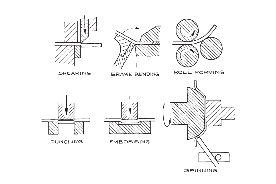
illustrated in Figure 1.8.
Sheet
metal is cut in a guillotine shear. Shears are
designed for making long straight cuts or for cutting out
inside corners. A typical shear can make a cut a meter
in length in sheet metal of up to 1.5 mm (1/16 in.) in
thickness.
A sheet-metal brake is used to bend sheet stock. A typ-
ical instrument-shop brake can accommodate sheet stock
at least a meter wide and up to 1.5 mm (1/16 in.) thick. The
minimum bend radius is equal to the thickness of the sheet
metal. Dimensional tolerances of 1 mm (.04 in.) can be
maintained.
Sheet can be formed into a simple curved surface on a
sheet-metal roll. The roll consists of three long parallel
rollers, one above and two below. Sheet is passed between
the upper roller and the two lower rollers. The upper roller
is driven. The distance between the upper roller and the
lower rollers is adjustable and determines the radius of the
curve that is formed.
Holes can be punched in sheet metal. A sheet-metal
punch consists of a punch, a guide bushing, and a die.
The punch is the male part. The cross section of the punch
determines the shape and size of the hole. The punch is a
close fit into the die, so that sheet metal placed between the
two is sheared by the edge of the punch as it is driven into
the die. Round and square punches are available in standard
sizes. A punch-and-die set to make a nonstandard hole
can be fabricated, but the cost may be justified only if a
large number of identical holes are required. On the other
hand, a very precisely shaped hole can be made in a punch-
and-die operation since the tools can be made with great
precision.
Sheet metal can be embossed with a stamp and die,
similar to a punch and die except that the die is somewhat
larger than the stamp, so that the metal is formed into the
die rather than sheared off at the edge.
Sheet metal can be formed into surfaces that are figures
of revolution by spinning. The desired shape is first turned
in hard wood in a lathe. A circular sheet-metal blank is
then clamped against the wooden form by a rubber-faced
rotating center mounted in the lathe tailstock. Then as
the wooden form is rotated the sheet metal is gradually
formed over the surface of the wood by pressing against
the sheet with a blunt wooden or brass tool. Spinning
requires few special tools and is economical for one-off
production.
1.1.8 Casting
Sand casting is the most common process used for the
production of a small number of cast parts. Although
10 MECHANICAL DESIGN AND FABRICATION
few instrument shops are equipped to do casting, most
competent machinists can make the required wooden pat-
terns that can then be sent to a foundry for casting in iron,
brass, or aluminum alloy. There are both mechanical and
economical advantages to producing some complicated
parts by casting rather than by building them up from
machined pieces. Very complicated shapes can be pro-
duced economically because the patternmaker works in
wood rather than metal. Castings can be made very rigid
by the inclusion of appropriate gussets and flanges that can
only be produced and attached with difficulty in built-up
work. Most parts on an instrument require only a few
accurately located surfaces. In this case the part can be
cast and then only critical surfaces machined.
A designer must understand the sand-casting process in
order to design parts that can be produced by this method.
A sand-casting mold is usually made in two parts, as
shown in Figure 1.9. The lower mold box, called the drag,
is
filled with sand, and the wooden pattern is pressed into
the sand. The sand is leveled and dusted with dry parting
sand. Then the upper box, or cope, is positioned over the
lower and packed with sand. The two boxes are separated,
the pattern is removed, and a filling hole, or sprue, is cut in
the upper mold. A deep hole can be cast by placing a sand
core in the impression, as shown in Figure 1.9(c). Note that
the
pattern has lugs, called core prints, which create a
depression to support the core. The two halves of the mold
are then clamped together and filled with molten metal.
It is obvious that a part to be cast must include no
involuted surfaces above or below the parting plane, so
that the pattern can be withdrawn from the mold without
damaging the impression. It is also good practice to taper
all protrusions that are perpendicular to the parting plane
to facilitate withdrawal of the pattern from the mold. A
Figure 1.8 Sheet-metal shop processes.
TOOLS AND SHOP PROCESSES 11
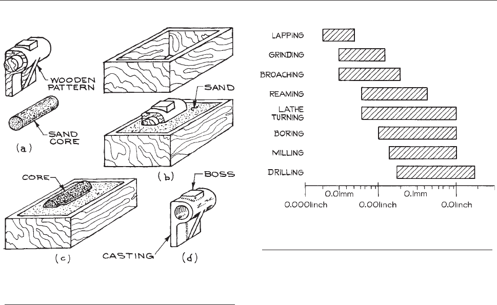
taper or draft of 1–2° is adequate. Surfaces to be machined
should be raised to allow for the removal of metal. That
is the purpose of the boss shown in Figure 1.9(d). When
possible,
all parts of the casting should be of the same
thickness to avoid stresses that may build up as the
molten metal solidifies. All corners and edges should be
radiused. With care, a tolerance of 1 mm (.03 in.) can be
maintained.
1.1.9 Tolerance and Surface Quality for
Shop Processes
The designer must decide on the precision and accuracy
required in making each part of an apparatus. Also a deci-
sion must be made about the quality of the surfaces of each
part to assure proper fit and function. It follows that the
capabilities of the various shop processes must be taken into
consideration, as well as the cost of production, to meet
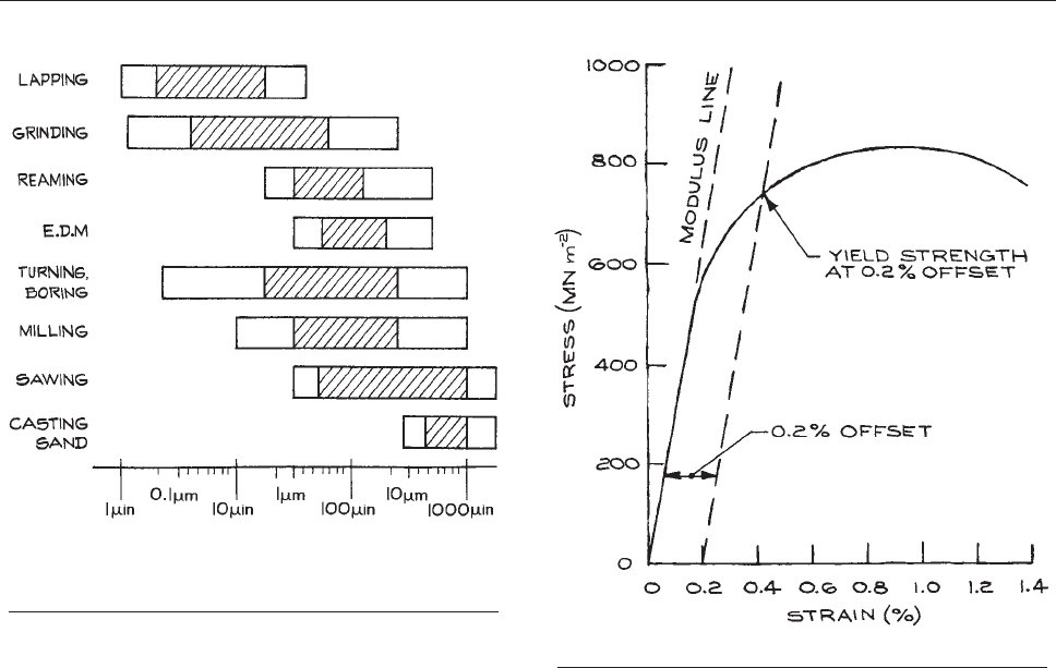
desired tolerances and surface quality (note Figure 1.45).
Prec
ision and accuracy are specified as the toler-
ance (+/) on each dimension of a part. The surface
roughness is specified as the RMS (Route Mean Squar ed)
variation in the height of a surface.
Figure 1.10 gives an approximate indication of the tol-
erance
normally obtainable for the shop processes dis-
cussed in this section. Figure 1.11 specifies the surface
quality
normally obtained in various shop process as well
in industrial processes used in the manufacturer of materi-
als from which parts are machined. An important point to
be made here is that it is often possible to use materials as
they come from the supplier without further machining of
the surfaces. It should be noted as well that obtainable
tolerances and surface quality depend upon the size of the
part being made. A tolerance of 60.05mm (6.002 in.)
is easily obtained in a milling operation on a part that is
only a few centimeters across. In a part that is 100 times
larger, a tolerance of 60.5 mm (6.02 in.) is the best that
can be obtained in a milling operation without the expen-
diture of considerable effort.
1.2 PROPERTIES OF MATERIALS
The materials employed in the construction of an appara-
tus – metals, plastics, glass, ceramic, ev en wood – are char-
acterized by their strength, flexibility, hardness, toughness,
Figure 1.9 Sand casting: (a) the pattern and core;
(b) making an impression in the lower mold box; (c) inserting
the sand core in the impression; (d) the finished casting.
Figure 1.10 Tolerance that can be reasonably maintained
in shop processes for a work-piece dimension of 1 to 10 cm.
(Adapted from ASME, ANSI Std. B4.1-1967)
12 MECHANICAL DESIGN AND FABRICATION
machinability, electrical and thermal conductivity, and so
on. In order to wisely choose a material for a part of an
apparatus, it is essential to understand the ways in which
these properties are specified, how these properties can be
modified by heating and working, and how to design to
best exploit these properties.
1.2.1 Parameters to Specify Properties of
Materials
The strength and elasticity of metal are best understood in
terms of a stress–strain curve such as is shown in Figure
1.12. Str
ess is the force applied to the material per unit of
cross-sectional area [MN m
2
, psi (pounds per square
inch)]. This may be a stretching, compressing, shearing,
or twisting force. Direct strain is the change in length per
unit length that occurs in response to an in-line stress
[strain is unitless (cm/cm, in/in) or expressible as a per-
cent]. Shear strain is the sideward displacement per unit
length in response to a transverse stress (again without
units). A torsional stress induces a shear strain. Most met-
als deform in a similar way under compression or elonga-
tion. When a stress is applied to a metal, the initial strain
is elastic and the metal will return to its original dimen-
sions if the stress is removed. Beyond a certain stress how-
ever, plastic strain occurs and the metal is permanently
deformed.
The tensile strength or ultimate strength of a metal is the
stress applied at the maximum of the stress–strain curve.
The metal is very much deformed at this point, so that in
most cases it is impractical to work at such a high load.
A more important parameter for design work is the yield
strength. This is the stress required to produce a stated,
small, plastic strain in the metal – usually 0.2% permanent
deformation. For some materials the elastic limit is specified.
This is the maximum stress that the material can withstand
without permanent deformation.
The slope of the straight-line portion of the stress–strain
curve is a measure of the stiffness of the material; this is the
modulus of elasticity, E, sometimes referred to as ‘‘Young’s
modulus.’’ It is worthwhile to note that E is about the same
Figure 1.11 Surface quality as RMS variation in surface
height for various machining and production processes.
(Adapted from ASME, ANSI Std. B46.1-1961)
Figure 1.12 Stress–strain curve for a metal.
PROPERTIES OF MATERIALS 13

for all grades of steel (about 210 GN/m
2
or 30 3 10
6
psi)
and about the same for all aluminum alloys (about 70
GN/m
2
or 10 3 10
6
psi), regardless of the strength or hard-
ness of the alloy. The effect of elastic deformation is
specified by Poisson’s ratio, l, the ratio of transverse con-
traction per unit dimension of a bar of unit cross-section to
its elongation per unit length, when subjected to a tensile
stress. For most metals, l ¼ 0.3. A modulus of elasticity in
shear or shear modulus, G, is similarly defined for a tor-
sional stress. The shear modulus is typically about one
third of Young’s modulus for a metal.
The hardness of a material is a measure of its resistance
to indentation and is usually determined from the force
required to drive a standard indenter into the surface of
the material or from the depth of penetr ation of an inden-
ter under a standa rdized f orce . The common hardness
scales used for metals are the Brinell hardnes s number
(BHN), the Vickers scale (VHN), and the Rockwell C
scale. Type 304 stai nless steel is about 150 B HN, 160
Vickers , or 0 Rockwell C. A file is 600 BHN, 650 Vic kers,
or 6 0 Rockwell C. The Shore hardness scale is deter-
mined by the heigh t o f rebo und o f a ste el b all dro ppe d
from a specified distance above the surface of a material
under tes t. Mineralogi sts and c eramic enginee rs use the
Mohs hardness scale. It is based upon standard materials,
each of which will scratch all materials below it on the
scale. Knoop hardness is used as a measure for very brit-
tle materials or thin sheets, where only a microindenta-
tion with a pyramidal diamond point can be made.
Figure 1.13 shows the approximate relation of the various
ha
rdness sca les .
A designer must consider the machinability of a mate-
rial before specifying its use in the fabrication of a part that
must be lathe-turned or milled. In general, the harder and
stronger a material, the more difficult it is to machine. On
the other hand, soft metals, such as copper and some nearly
pure aluminum alloys, are also difficult to machine
because the metal tends to adhere to the cutting tool and
produce a ragged cut. Some metals are alloyed with other
elements to improve their machinability. Free-machining
steels and brass contain a small percentage of lead or sul-
fur. These additives do not usually affect the mechanical
properties of the metal, but since they have a relatively
high vapor pressure, their out-gassing at high temperature
can pose a problem in some applications.
1.2.2 Heat Treating and Cold Working
The properties of many metals a nd metal al loys ca n be
considerably changed by heat treating or cold working to
modify the chemical or mechanical nature of the granular
structure of the metal.
2
The e ffect of heat treatment
depends u pon the te mpe rat ure to which th e m ate ria l is
heated relative to the temperatures at which phase tran-
sitions occur in the metal, and the rate at which the metal
is cooled. If the metal is heated above a transition temper-
ature and quickly cooled or quenched, the chemical and
physical structure of the high-temperature phase may be
frozen in, or a transition to a new metastable phase may
occur. Que nching is acc omplished by plunging the heated
part into w ater or o il. This proc es s is usually ca rried out to
harden the metal. Hardened metals can be softened by
annealing, wherein the metal is h eated above the transi-
tion temperature and then slowly cooled. It is frequently
desirable to a nneal hardened metals before machining
and re-harden after working, although hardening and
annealing can result in distortion, owing to differences
in density of the high and low temperature phases. Temper-
ing is an intermediate heat treatment wherein previously
hardened metal is reheated to a temperature below the tran-
sition point in order to relieve stresses and then cooled at a
rate that preserves the desired properties of the hardened
material.
Repeated plastic d eformation w ill reduce the size of
the grai ns or crystallites within the metal. This is cold
working that accompanies bending, rolling, drawing, ham-
mering, and, to a lesser extent, cutting operations. Not
all metals benefit from cold working, but for some the
strength is greatly increased. Because of the annealing
effect, the strength and hardness derived from cold work-
ing begin to disappear as a metal is heated. This occurs
above 250 °C for steel and above 125 °C for aluminum. In
rolling or spinning operations, some metals will work-
harden to such an extent that the material must be periodi-
cally annealed during fabrication to retain its workability.
Cold working reduces the toughness of metal. The surface
of a metal part can be work-hardened, without modifying
the internal structure, by peening or shot blasting and by
some rolling operations. The strength of metal stock may
depend upon the method of manufacture. For example,
14 MECHANICAL DESIGN AND FABRICATION
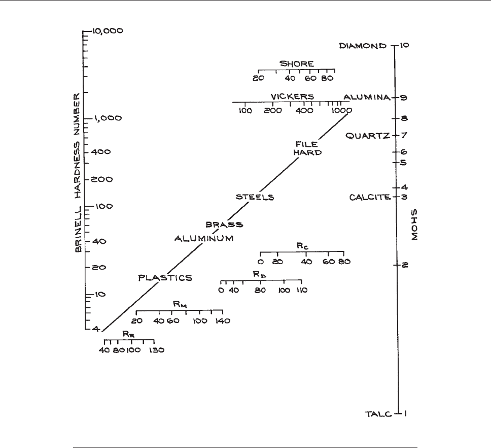
sheet metal and metal wire are usually much stronger than
the bulk metal because of the work hardening produced by
rolling or drawing.
The surface of a metal part may be chemically modified
and then heat-treated to increase its hardness while retain-
ing the toughness of the bulk of the material beneath. This
process is called case hardening. The many methods of
case hardening are usually named for the chemical that
is added to the surface. Carburizing (C), cyaniding (C
and N), and nitriding (N) are common processes for case-
hardening steel. Of these, carburizing of low-carbon steel is
most conveniently performed in the lab or shop. The part to
be hardened is packed in bone charcoal or Kasenit in an
open metal box and heated in a furnace to 900 °C (salmon-
red heat). The time in the furnace, from 15 minutes to
several hours, determines the depth of the case. Steel will
absorb carbon by this process to a maximum depth of about
0.4 mm (0.015 in.) The part is removed from the furnace
Figure 1.13 Approximate relation of Brinell (BHN), Rockwell (R
R
,R
M
,R
B
,R
C
), Vickers
(VHN), Shore, and Mohs hardness scales.
PROPERTIES OF MATERIALS 15
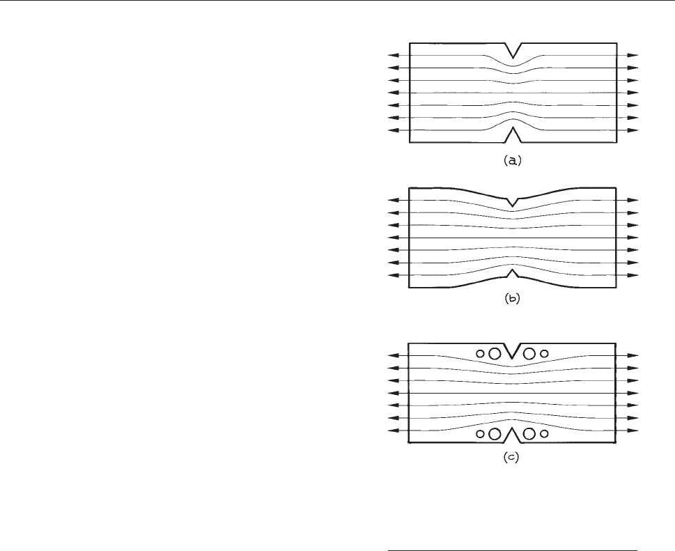
and promptly quenched in water. The quenching hardens
the case, but the core remains tough and ductile.
1.2.3 Effect of Stress Concentration
In choosing a material for a particular job, one must con-
sider not only the stress the part is expected to bear, but
also the way in which the stress is distributed. Careless
design can lead to failure in very strong materials under
relatively light loads if the stress of the load is concentrated
in a small volume.
An abrupt change in the cross-section of a loaded beam
or shaft produces a concentration of stresses, as shown in
Figures 1.14(a) and 1.15(a). For the element in tension
[Figure 1.14(a)] the lines indicate the direction of tensile
force;
this is a so-called ‘‘force flow depiction.’’ For an
element under torsional stress, Figure 1.15(a), the lines
indicate
the cross-section of concentric cylindrical shells
each under the same torque. Stress increases when the force
flow lines or equitorque surfaces become sharply curved
and crowded together . Stress concentrations are located at
steps, grooves, keyways, holes, dents, and scratches. Failure
occurs as a result of shear forces in the region of highest
stress concentration. Anyone who has ever broken a bolt is
familiar with this effect; a bolt invariably fails at the step
where the head joins the shaft. The effects of stress concen-
tration may be especially important in fatigue failure result-
ing from cyclic applications of stress.
Stress is often concentrated in the area of the smallest
radius of curvature of a part, as suggested in Figures
1.14(a) and 1.15(a). This observation explains the manner
in
which a crack propagates once a part has begun to fail:
the radius of curvature is small at the end of a crack, thus
stress is concentrated at the tip of the crack and further
failure ensues. Increasing the radius of curvature of a stress
riser can mitigate stress concentration. It is often more
practical to introduce features that move the force flow
lines away from the stress riser when it is not possible to
modify the offending aspect. Examples are given in Fig-
ures
1.14 and 1.15.
Threaded
parts are often a problem. The ‘‘V’’ bottom of
the thread groove is an insipient stress riser. As suggested
in Figure 1.16, reducing the diameter of the adjoining
unthreaded
portion of a shaft has the effect of moving
the equitorque surfaces away from the threads.
There are a number of means of detecting stress in a
part. One of the most useful is the photoelastic method.
3
In
this technique a transparent plastic model is stressed in the
same way as the element of interest without necessarily
duplicating the magnitude of the stress. The model is illu-
minated with polarized, monochromatic light and viewed
through a polarizer. As shown in Figure 1.17, the stress
distrib
ution appears as fringes in the image; closely spaced
fringes characterize stress concentrations. Most glassblow-
ing shops are equipped with a polarizing device of this type
for detecting residual stresses in worked glass (see Figure
2.16, next chapter).
Figure 1.14 Force flow lines in a beam under
stress: (a) A notch in a beam under tension
concentrates stress in the vicinity of the notch.
(b) and (c) suggest means to mitigate the stress
concentration.
16 MECHANICAL DESIGN AND FABRICATION
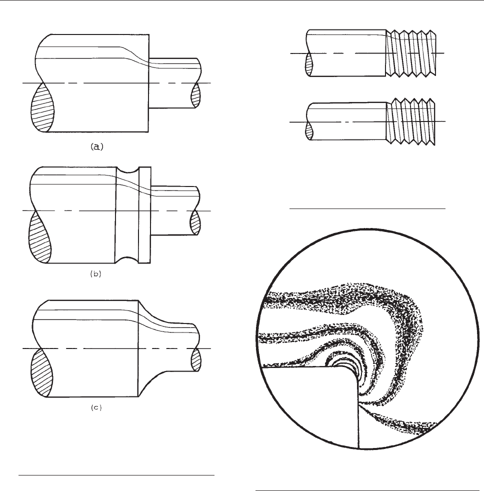
In a similar fashion, fabricated parts can be nondestruc-
tively tested by means of holography. A hologram of the
object is made; then the part is stressed and a second holo-
gram is made. The two holograms are then superposed and
placed in the holographic projector. The resulting three-
dimensional image consists of patterns of fringes that are
densest in the areas of greatest distortion in the stressed
object. Holographic nondestructive testing (HNDT) is car-
ried out as a commercial service.
Figure 1.15 A shaft under torsional stress. Lines
indicate concentric equitorque surfaces: (a) A step in
a shaft under a torsional load concentrates stress in
the vicinity of the step. (b) and (c) suggest means to
mitigate the stress concentration.
Figure 1.16 Threads on a shaft may
produce a concentration of stress.
Reducing the diameter of the adjoining
shaft moves the equitorque surfaces
away from the threads.
Figure 1.17 Stress distribution in a transparent plastic
model as observed when the part is illuminated with
polarized light and observed with a crossed polarizer.
PROPERTIES OF MATERIALS 17

A particularly simple and inexpensive means of locating
stress concentrations in a working part has been developed
by Magnaflux. The part to be tested is sprayed with a
substance that forms a hard, brittle layer over the surface.
The part is returned to service for a time, and any flexing of
the part causes the surface coating to crack. The part is
then removed and dipped in a dye that permeates the
cracks to reveal the areas where the strain under load
was greatest.
1.3 MATERIALS
We shall discuss in a qualitative manner the properties of
useful metals, plastics and ceramics. Quantitative data are
gathered together in Table 1.3.
1.3.1 Iron and Steel
For instrument work, iron is used primarily as a casting
material. The advantages of cast iron are hardness and a
high degree of internal damping. Cast iron is harder than
most steels and is used for sliding parts, where resistance
to wear is important. The damping capacity of iron, that is,
the ability to dissipate the energy of vibration, is about 10
times that of steel and for this reason the frame of a del-
icate instrument is often made of cast iron.
Cast iron contains a few % carbon. The carbon is in a
free state in gray cast iron, while it is chemically incorpo-
rated into the structure of white cast iron. Gray iron is
inexpensive and easy to machine. Class-30 gray iron has
a Brinell hardness of about 200 BHN. It is, however, rather
brittle and is only about half as strong as steel. White iron
is stronger and harder than gray iron, and thus it is very
wear-resistant. White iron is difficult to machine and is
usually shaped by grinding. The machinability and ductil-
ity of cast irons can be considerably improved by various
heat treatments.
Steel is an iron alloy. There are more than 10 000 differ-
ent types of steel. Steels are classed as cast or wrought
steels depending on the method of manufacture. Wrought
steels are produced by rolling and are almost the only kind
used for one-off machine work. Steels are also classified as
either carbon steels or alloy steels. Carbon steels are
specified by a four-digit number. Plain carbon steels are
specified as 10xx, where xx is a two-digit number that
indicates the carbon content in hundredths of %. In general
the strength and hardness of carbon steel increases with
carbon content, but these properties also depend upon the
nature of the heat treatment and cold working that the
metal has received. Alloy steels containing elements in
addition to carbon have special properties especially useful
for the manufacture of tools and dies. These include, for
example, manganese steels (designated 13xx for tool steel
with 1.8% Mn), nickel alloy steel (23xx, 3.5% Ni; 25xx,
5% Ni), molybdenum steel (40xx, 0.20 % Mo), and so on.
Steels with a carbon content in the 0.10–0.50% range
are referred to as low- and medium-carbon steels or mild
steels. These steels are supplied rolled or drawn and are
most suitable for machine work.
High-carbon steels are difficult to machine and weld,
although their machinability is improved if they are first
annealed by heating to 750 °C (orange heat) and cooling
slowly in air. They may be returned to their hard state by
reheating to 750 °C and quenching in water; however, this
process inevitably produces some distortion.
The most common alloy steels are the types known as
stainless steels. The main constituents of stainless steels
are iron, chromium, and nickel. They are classified as fer-
ritic, martensitic, or austenitic, depending on the nickel
content. The high-nickel austenitic alloys comprise the
200 and 300 series of stainless steels. 300-series stainless
steels are most useful for instrument construction because
of their superior toughness, ductility, and corrosion resist-
ance. The austenitic stainless steels are sensitive to heat
treatment and cold working, although the heat-treatment
processes are rather more complicated than for plain car-
bon steels. For example, quenching from 1000 °C leaves
these steels soft. Cold working, however, can more than
double the strength of the annealed alloy. The heat asso-
ciated with welding of austenitic stainless steels can result
in carbide pr ecipitation at the grain boundaries in the vicinity
of a weld, leaving the weld subject to attack by corrosive
agents. The carbides can be returned to solution by annealing
the steel after welding. There are also some special stainless
steels that do not suffer from carbide precipitation. In general,
stainless steels are more expensi v e than plain carbon steels,
but their superior qualities often of fset the extra cost.
Type 303 is the most machinable of the 300-series
alloys. Type 316 has the greatest resistance to heat and
18 MECHANICAL DESIGN AND FABRICATION

Table 1.3 Properties of Research Materials
Material Density
(kg m
3
)
Yield
Strength
(MN m
2
)
Tensile
Strength
(MN m
2
)
Modulus
of Elasticity
(GN m
2
)
Shear
Modulus
(GN m
2
)
Hardness
a
Coefficient
of Thermal
Expansion
(10
6
K
1
)
Comments
Ferrous Metals
Cast gray
iron (ASTM 30)
6990 170 210 90 36 200 BHN 11
1015 steel (hot-finished) 7850 190 340 200 76 100 BHN 15 Low carbon (0.15% C)
1030 steel (hot-finished) 7850 250 470 200 76 137 BHN 15 Medium carbon
(0.30% C)
1050 steel (hot-finished) 7850 340 620 200 76 180 BHN 15 High carbon
(0.50% C)
Type 304 stainless
steel (annealed)
7910 240 590 190 69 150 BHN 17 Austenitic
Type 304 stainless
steel (cold-worked)
7910 520 760 190 69 240 BHN 17 Austenitic
Type 316 stainless
steel (cold-worked)
7910 410 620 190 69 190 BHN 16 Austenitic
Nickel Alloys
Monel 400: 25 °C 8820 170 480 110 BHN 14 Slightly magnetic
500 °C 150 310 180 16
Monel 500: 25 °C 8460 280–1000 600–1200 14 Nonmagnetic
500 °C 620 65 180 140 BHN 16
Inconel 600: 25 °C 8400 250 620 210 12 Strong, resists
high-temperature
oxidation
650 °C 180 450 140 120 BHN 16
Invar (0–100 °C) 8130 160 480 140 140 BHN 1.3 small temperature
coefficient
Aluminum Alloys
1100-0 2760 30 90 70 30 23 BHN 23 99% Al
2024-T4 2710 320 470 70 30 120 BHN 23 3.8% Cu, 1.2% Mg,
0.3% Mn
2024-T4 (200 °C) 2710 80 120
6061-T6 2760 280 310 70 30 95 BHN 23 0.15% Cu, 0.8% Mg,
0.4% Si
7075-T6 2790 500 570 70 30 150 BHN 23 5.1% Zn, 2.1% Mg,
1.2% Cu
Copper Alloys
Yellow brass (annealed) 8460 410 510 100 40 20 65% Cu, 35% Zn
Yellow brass
(cold-worked)
8460 410 510 100 40 150 BHN 20 65% Cu, 35% Zn
Cartridge brass (1/2 hard) 8510 360 480 110 40 145 BHN 20 70% Cu, 30% Zn
Beryllium copper
(precipitation-hardened)
8210 960 1200 130 48 380 BHN 17 98% Cu, 2% Be
MATERIALS 19

corrosion. All of these alloys are fairly nonmagnetic; types
304 and 316 are the least magnetic. Machining and cold
working tends to increase the magnetism of these alloys.
Residual magnetism can be relieved by heating to 1100 °C
[safely above the temperature range (450–900°) where
carbide precipitation occurs] and quenching in water. Thin
pieces that might distort excessively may be quenched in
an air blast.
1.3.2 Nickel Alloys
Nickel alloys are typically tough and strong, and resistant to
corrosion and oxidation. The machining characteristics of
the wrought alloys are similar to those of steel, and they are
readily brazed and welded. Nickel alloys mostly do not go
by a standard specification like steel, but rather are referred
to by trade names. These names often allude to an alloy or
Table 1.3. (contd.)
Material Density
(kg m
3
)
Yield
Strength
(MN m
2
)
Tensile
Strength
(MN m
2
)
Modulus
of Elasticity
(GN m
2
)
Shear
Modulus
(GN m
2
)
Hardness
a
Coefficient
of Thermal
Expansion
(10
6
K
1
)
Comments
Unalloyed Metals
Copper 8930 70 220 110 45 44 BHN 17
Molybdenum 10200 560 650 320 120 190 VHN 5.4 Refractory, nonmagnetic
Tantalum 16590 330 460 180 70 80 VHN 6.5 Refractory, somewhat
ductile
Tungsten 19270 1520 1520 410 150 350 VHN 5 Refractory, very dense
Plastics
Phenolics 1350 50 7 125 R
M
81 Bakelite, Formica
Polyethylene (low density) 910 10 0.2 10 R
R
180
Polyethylene (high density) 940 30 0.8 40 R
R
216
Polyamide 1110 80 2.8 118 R
R
90 Nylon
Polymethylmethacrylate 1190 50 2.9 90 R
M
72 Lucite, Plexiglas
Polytetrafluoroethylene 2130 20 0.4 60 R
R
99 Teflon
Polychlorotrifluoroethylene 2100 40 1.7 110 R
R
70 Kel-F
Poly(amide-imide) 1440 150 5.8 80 R
E
28 Torlon < 200 °C
to 220 °C
Polyimide 1440 80 2.6 45 R
R
54 Vespel 270 °Cto
290 °C
Polycarbonate 1190 60 2.3 70 R
M
70 Lexan
Ceramics
Alumina (polycrystalline) 3900 240 330 9 Mohs 8 99% alumina
Macor 2520 30 60 25 400 VHN 13 Corning machinable
ceramic
Steatite 3590 60 100 10.6
Wood
Douglas fir (air-dried) 300 65,3
b
10 6,35
b
Typical of softwoods
Oregon white
oak (air-dried)
700 70,6
b
16 5,55
b
Typical of hardwoods
a
BHN ¼ Brinell hardness number; R ¼ Rockwell hardness; VHN ¼ Vickers hardness.
b
Parallel to fiber, across fiber.
20 MECHANICAL DESIGN AND FABRICATION

class of alloys that have been designed to optimize a partic-
ular property. Nickel alloys are expensive compared to alloy
steels, but not so much so that they shouldn’t be used when
an instrument can exploit their special properties.
The Monel alloys are nickel–copper alloys whose prop-
erties make them a better choice than austenitic stainless
steels in some applications. The most familiar is Monel
400. It is resistant to attack by both acids and bases and
is sufficiently ductile for parts to be fabricated by spin-
ning and stamping. Monel 404 is similar, but it is quite
nonmagnetic, and its magnetic properties are not affected
by cold working. Monel 500 is similarly nonmagnetic and
retains most of its strength up to 500 °C.
Inconel alloys are notable for their strength at high tem-
peratures. The Inconel 600 series of alloys retain their
strength to 700 °C and are very resistant to oxidation at
high temperatures. Inconel 600 is nonmagnetic. The Inconel
700 series are so-called ‘‘superalloys’’ with tensile strengths
on the order of 1000 MN m
2
(150 000 psi). They are used
in highly-stressed parts that will maintain their strength to
1000 °C. They must be heat-treated to obtain the maximum
high-temperature strength. The Inconel 700 alloys, espe-
cially Inconel 702 and Inconel X-750, are nonmagnetic.
The Hastelloy alloys, of which Hastelloy B is most com-
mon, contain primarily nickel and molybdenum and are nearly
as strong as the Inconel 700 alloys and somewhat more duc-
tile. These alloys are notable for their resistance to corrosion.
In certain instances the dimensions of a component of an
instrument must be very stable in the face of variations of
temperature. Iron–nickel alloys containing about 36%
nickel have been found to meet this requirement. Invar
(Carpenter Technology Corp.) is one such alloy. This
material has a coefficient of expansion of 1.3 3 10
6
K
1
in the range 0 to 100 °C and about twice this at temper-
atures up to 200 °C. Better yet, the alloy Super-Invar (from
Eagle Alloys or High Temp Metals) has a coefficient of
0.3 3 10
6
K
1
in the range 0 to 100 °C. By comparison,
the coefficient of expansion of stainless steel is about
1.5 3 10
5
K
1
. One disadvantage of Invar in certain
applications is that it is magnetic below 277 °C.
After being machined, Invar may require stress relieving
to achieve maximum stability. Rosebury
4
suggests the fol-
lowing heat treatment: heat to about 350 °C for one hour
and allow to cool in air; heat to a temperature slightly above
the operating temperature and cool slowly to a temperature
below the operating temperature; repeat step 2. To achieve
the minimum coefficient of thermal expansion for Super-
Invar, Eagle Alloys recommendthefollowingheat treatment:
hold at 830 °C for 10 minutes, quench rapidly in water or
with an air blast; hold at 315 °C for 60 minutes and then air
cool; hold at 100 °C for 24 hours and then air cool.
Kovar is an iron–nickel–cobalt alloy designed for mak-
ing metal-to-glass seals. Its thermal expansion character-
istics match that of several hard glasses including Corning
7052 and 7056. Unfortunately, Kovar is magnetic and
easily oxidized.
1.3.3 Copper and Copper Alloys
Copper is a soft, malleable metal. Of all metals (short of the
noble metals) it is the best electrical and thermal conductor.
For instrument applications, oxygen-free high-conductivity
(OFHC) copper is preferred because of its high purity and
excellent conductivity and because it is not subject to hydro-
gen embrittlement (see p. 33). Ordinary copper becomes
brittle and porous when exposed to hydrogen at elevated
temperatures such as may occur in welding or brazing.
Alloys of copper are classified as either brasses or
bronzes. Brass is basically an alloy of copper and zinc.
Generally, brass is much easier to machine than steel but
not quite so strong, and its electrical and thermal coeffi-
cients are about half those of pure copper. Its properties
vary considerably with the proportions of copper to zinc,
and also with the addition of small amounts of other ele-
ments. Soldering or brazing readily joins brass parts. Brass
is expensive, but, because it is easy to work, it is well
suited to instrument construction, where the cost of fabri-
cation far outweighs the cost of materials.
For general machine work, yellow brass (35% Zn) is most
suitable. Free-machining brass is similar except that it con-
tains 0.5–3% lead. Cartridge brass (30% Zn) is very ductile
and is suitable for the manufacture of parts by drawing and
spinning, and for rivets. It work-hardens during cold form-
ing and may require periodic annealing to 600 °C. Stresses
that have built up in a cold-formed part during manufacture
can be relieved by heating to 250 °C for an hour.
The name bronze originally meant an alloy of copper
and tin, but the term now also refers to alloys of copper
and many other elements, such as aluminum, silicon,
beryllium, or phosphorus. Bronzes, generally harder and
MATERIALS 21

stronger than brasses, often are of special value to the
designer of scientific apparatus. Beryllium copper or
beryllium bronze is a versatile material whose properties
can be considerably modified by heat treatment. In its soft
form it has excellent formability and resistance to fatigue
failure. Careful heat treating will produce a material that
is harder and stronger than most steels. It is useful for the
manufacture of springs and parts that must be corrosion-
resistant. Also it is nearly impossible to strike a spark on
beryllium bronze; this makes it useful for parts to be used
in an explosive atmosphere. Beryllium bronze hand tools
are available for use around explosive materials. Phosphor
bronze cannot be heat-treated, but it is very formable and
has great resistance to fatigue. It is used for bellows and
springs. Aluminum bronze is highly resistant to corrosion
and is strong and tough. It is used in marine applications.
Bronze stock can be manufactured by sintering. Compact-
ing and heating a bronze powder at a temperature below
the melting point produces sintered bronze. It is quite
porous in this form and can be used as a filter or can be
impregnated with lubricant for use as a bearing.
1.3.4 Aluminum Alloys
Aluminum alloys are valued for their light weight, good
electrical and thermal properties, and excellent machina-
bility. Aluminum is about one third as dense as steel. Its
electrical conductivity is 60% that of copper, but it is a
better conductor per unit weight.
Aluminum is resistant to most corrosive agents except
strong alkalis, owing to an oxide film that forms over the
surface. This layer is hard and tenacious, and forms nearly
instantaneously on a freshly exposed surface. Because the
oxide layer is an insulator, electrical connections to alumi-
num parts are problematic. In some applications aluminum
parts can accumulate a surface charge. This problem can
be overcome by copper- or gold-plating critical surfaces.
The oxide layer makes plating difficult, but reliable plating
can be carried out by specialty plating shops. Aluminum
parts cannot be easily soldered or brazed (see, however,
Handy & Harman AL802 flux-cored aluminum solder).
Heliarc or TIG (tungsten inert gas) welding is quite practical
with aluminum (see, for example, the plethora of welded-
aluminum-frame bicycles on the market). Welds in alumi-
num tend to be porous, and welding weakens the metal in
the vicinity of the weld because of the rapid conduction of
heat into the surrounding metal during the operation.
Aluminum stock is produced in cast or wrought form.
Wrought aluminum, produced by rolling, is used for most
machine work. A four-digit number that indicates the com-
position of the alloy, followed by a suffix, beginning with T
or H that specifies the state of heat treatment or work hard-
ness, specifies aluminum alloys. The heat-treatment scale
extends from T0 through T10. T0 indicates that the mate-
rial is dead soft, and T10 that it is fully tempered. The
1000-series alloys are more than 99% aluminum. The
2000-series alloys are aluminum alloyed with copper.
The 6000-series alloys contain magnesium and silicon.
The 7000-series are alloys with zinc. Readily available
stock includes 1100-T0, a soft, formable alloy that is
nearly pure aluminum and is used for extrusions. 2024-
T4 or -T6 is as strong as annealed mild steel and is used
for general machine work. 6061-T6 is not quite so strong
as 2024-T4, but is more easily cold-worked. Its machina-
bility is excellent. The strongest readily available alumi-
num alloy is 7075-T6. It is easily machined; its corrosion
resistance, however, is inferior to that of other alloys.
Aluminum is available as plate, bar, and round and
square tube stock. Aluminum jig plate is useful for instru-
ment construction. This is rolled plate that has been fly-cut
by the manufacturer to a high degree of flatness.
Aluminum may be anodized to give it a pleasing appear-
ance and to improve corrosion resistance. Anodizing of
aluminum is carried out inexpensively by most commer-
cial plating services. A number of proprietary formulas,
such as Birchwood-Casey AlumaBlack, are available to
blacken aluminum to reduce its reflectivity. Beware, how-
ever, of difficulties in making a reliable electrical connec-
tion to an anodized aluminum surface.
1.3.5 Other Metals
Magnesium alloys are useful because their density i s only
0.23 times that of steel. Magnesium is very stiff per unit
weight, and is completely nonmagnetic. It is very easy
to machine, although there is a fire hazard. Magnesium
chips can be ignit ed, but not the bulk material. The
strength of magnesium alloys is considerably reduced
above 100 °C. The cost of these alloys is at least 10 times
that of steel.
22 MECHANICAL DESIGN AND FABRICATION

Titanium is about half as dense as steel, while titanium
alloys are stronger than steel. Titanium is very resistant
to corrosion and completely nonmagnetic. It is readily
machined, if one proceeds slowly with sharp carbide-
tipped cutters, and can be welded under an inert gas atmos-
phere. Titanium and titanium alloys (99%) are useful for
extreme-temperature service, since they maintain their
mechanical properties from –250 °C to well above 400 °C.
A titanium–manganese alloy (Ti-8Mn; 6.5–9% Mn) retains
a tensile strength greater than 100 000 psi to temperatures
in excess of 400 °C. Its strength and hardness (up to 36 R
c
)
can be varied considerably by heat treatment. Titanium–
aluminum–vanadium alloy (Ti-6Al-4V; 5.5–6.7% Al; 3.5–
4.5% V) is a similarly strong, versatile material. These
alloys are more easily machined than unalloyed titanium.
Titanium fasteners are available.
Molybdenum is a refractory metal. It exhibits a very low,
uniform, surface potential and is used for fabricating elec-
trodes and electron-optical elements. Molybdenum is brittle
and must be machined slowly using very sharp tools.
Molybdenum is produced from a melt or from a sintered
powder. The sintered stock is very difficult to machine.
Tungsten is the most dense of the readily available ele-
ments. Its density is 2.5 times that of steel. Compact coun-
terweights in scientific mechanisms are often made of
this material. Tungsten is also used for extreme high-
temperature service, such as torch nozzles and plasma
electrodes. Suppliers of refractory metals such as tungsten
and molybdenum include A. D. Mackay and Philips Elmet.
1.3.6 Plastics
Plastics are classified as either thermoplastic or thermoset-
ting. Within limits, thermoplastics can be softened by heat-
ing and will return to their original state upon cooling.
Thermosetting plastics undergo a chemical change when
heated during manufacture, and they cannot be re-softened.
Phenol-formaldehyde plastics, or phenolics, are the
most widely used thermosetting plastics. Phenolics are
hard, light in weight, and resistant to heat and chemical
attack. They make excellent electrical insulators. Phe-
nolics are usually molded to shape in manufacture and
typically incorporate a paper or cloth filler. Thus rein-
forced, the phenolic plastics are easily sawn and drilled.
Bakelite is a linen-reinforced phenolic plastic.
Representative thermoplastics include polyethylene,
nylon, Delrin, Plexiglas, Teflon, and Kel-F.
Polyethylene is inexpensive, machinable, and very
resistant to attack by most chemicals. It is soft and not
very strong. Its physical properties vary with the molecular
weight and the extent of chain branching within the poly-
mer. It is produced in high-density and low-density forms
that are whitish and translucent, respectively. It is also
manufactured in a blackened form that is not degraded
by ultraviolet radiation, as is the white form. Polyethylene
softens at 90 °C and melts near 110 °C. It can be welded
with a hot wire or a stream of hot air from a heat gun. It can
be cast, although it shrinks a great deal upon solidifying.
Care must be exercised when heating polyethylene
because it will burn. Polyethylene is an excellent electrical
insulator, with a dielectric strength of 40 000 V/mm [1000
V/mil (0.001 in.)].
Nylon, a polyamide, is strong, tough, and very resistant
to fatigue failure. It retains its mechanical strength up to
about 120 °C. It does not cold-flow, and is self-lubricating
and thus is useful for all types of bearing surfaces. Nylon is
available as rod and sheet in both a white and a black form.
Nylon balls and gears are also readily available. There
is no fire hazard with nylon, since it is self-extinguishing.
It is hygroscopic, and its volume increases and strength
decreases somewhat when moisture is absorbed.
Delrin is a polyacetal resin with properties similar to
hard grades of nylon in most respects, except that it is
not hygroscopic.
All plastics are electrical insulators, although the hygro-
scopic ones are liable to surface leakage currents. DuPont
produces a polyamide film known as Kapton that is
widely used as an electrical insulator. This material has a
high dielectric strength in thin films. It is strong and
tough, resists chemicals and radiation, and is a better ther-
mal conductor than most plastics. It is used in sheets as an
insulator between layers of windings in magnets. Kapton-
insulated wire is available. DuPont also supplies bulk
polyamide in standard shapes under the trade-name Vespel.
This material is relatively hard, strong, and machinable.
It is probably the best plastic material for use in vacuum
because of its low vapor pressure and its high-temperature
stability. Amoco produces a line of engineering plastics
under the name Torlon that are based upon poly(amide-
imide) copolymer. These thermoplastics are very strong
MATERIALS 23

and can be used up to 250 °C. Torlon is also an excellent
choice when plastics must be used in vacuum.
Plexiglas, Lucite, and Perspex are all trade names for
polymethylmethacrylate (PMMA). These materials, also
known as acrylic plastics, are strong, hard, and transparent.
Because they are machinable, heat-formable, and shatter-
resistant, polymethylmethacrylates are used in many appli-
cations as replacements for glass.
Thermoforming of acrylic sheet into curved surfaces is a
fairly simple operation. Begin with a wooden or metal
pattern of the desired shape. Rest the sheet on top of the
pattern, warm the plastic to about 130 °C, and permit grav-
ity to pull the softened sheet down over the form. The
forming may be done in an oven, or the plastic may be
heated with infrared lamps or with hot air from a heat gun.
It is necessary to apply the heat slowly and uniformly.
Polymethylmethacrylate dissolves in a number of
organic solvents. Parts can be cemented by soaking the
edges to be joined in acetone or methylene chloride for
about a minute and then clamping the softened edges
together until the solvent has evaporated.
General Electric manufactures a polycarbonate plastic
known as Lexan. It is transparent and machinable, it has
excellent vacuum properties, and is so tough as to be nearly
unbreakable. It is the preferred plastic replacement for
window glass. Lexan is one of the most useful plastics
for instrument construction.
Teflon is a fluorocarbon polymer. It is only slightly
stronger and harder than polyethylene, but it is useful at
sustained temperatures as high as 250 °C and as low as
–200 °C. Teflon is resistant to all chemicals, and nothing
will stick to it. In most applications it is not as good as
nylon as a bearing surface, since it tends to cold-flow away
from the area where pressure is applied. A thin film of
Teflon, such as is found on modern cookware, provides
dry lubrication and prevents dust and moisture adhesion.
Specialty shops that serve the food industry can apply
these films. Teflon is about ten times as expensive as nylon.
Kel-F is a fluorochlorocarbon polymer. Its chemical
resistance is similar to Teflon, but it is much stronger
and harder. Like Teflon, Kel-F does not absorb water.
A number of rubber-like polymeric materials, known as
elastomers, find application in scientific apparatus. Materials
of interest include Buna-N, Viton-A, and RTV. Buna-N is a
synthetic rubber. It can be used at sustained temperatures up
to 80 °C without suffering permanent deformation under
compression. It is available as sheet or in block form. It is
useful as a gasket material and for vibration isolation. Viton-
A is a fluorocarbon elastomer similar in appearance and
mechanical properties to Buna-N. Useful up to 250 °C, it
tends to take a set at higher temperatures. Unlike Buna-N,
Viton-A shows no tendency to absorb water or cleaning
solvents. RTV, a self-curing silicone rubber produced by
General Electric, comes in a semiliquid form and cures to
a rubber by reaction with moisture in the air. It is useful as a
sealant, a potting compound for electronic apparatus, and an
adhesive. It can be cast in a plastic mold.
1.3.7 Glasses and Ceramics
Borosilicate glasses such as Corning Pyrex 7740 or Kimble
KG-33 are used extensively in the lab. These glasses are
strong, hard, and chemically inert, and they retain these
properties to 500 °C. As will be discussed in the succeed-
ing chapter, they are conveniently worked with a natural-
gas–oxygen flame.
Quartz or fused silica has a number of unique properties.
It has the smallest known coefficient of thermal expansion
of any pure material: 1 3 10
6
K
1
. By comparison, the
thermal expansion coefficient of the borosilicate glasses
is 3 3 10
6
K
1
, and that of steel is 15 3 10
6
K
1
. Quartz
can be drawn into long, thin fibers. The internal damping in
these fibers is very low, and their stress–strain relation for
twisting is linear to the breaking point. Springs of quartz
fibers provide the best possible realization of Hooke’s law.
Torsion springs and coil springs made of a quartz fiber are
used in delicate laboratory balances. Quartz retains its
excellent mechanical properties up to 800 °C. It softens at
1500 °C and hence can only be worked with a hydrogen–
oxygen flame.
Alumina (Al
2
O
3
) is the most durable and heat-resistant of
the readily available ceramics. Only diamond, borazon, and
a fe w exotic metal carbides are harder. The compressive
strength of alumina exceeds 2000 MN/m
2
(300 000 psi),
although its tensile strength and shear strength are some what
less than those of steel. Alumina is brittle and, because of its
hardness, it ordinarily is shaped or cut by grinding with a
diamond-grit wheel. Alumina rod, tube, thermocouple wells,
and electrical insulators are av ailable. These shapes are pro-
duced by molding a slurry of alumina powder and various
24 MECHANICAL DESIGN AND FABRICATION
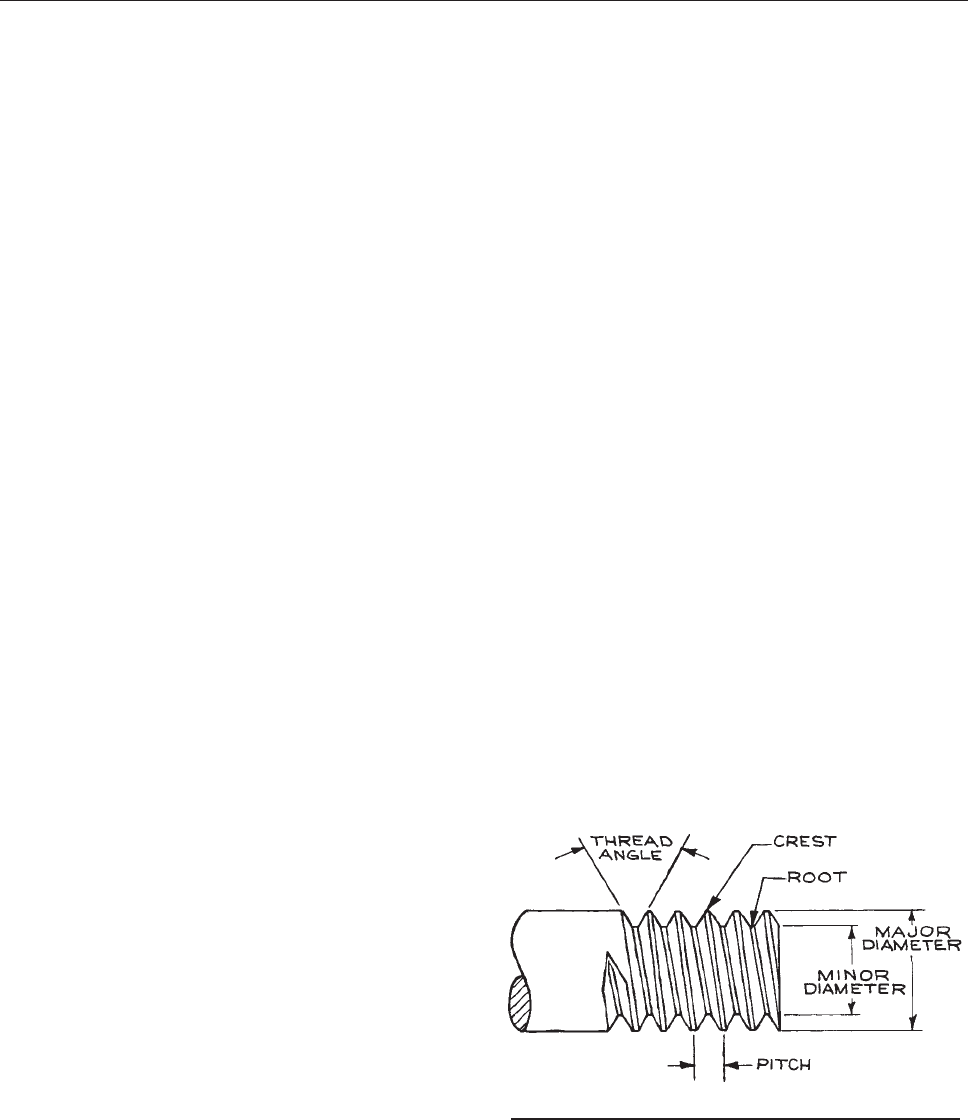
binders to the desired shape and then firing at high temper-
ature to produce the hard ceramic. One particularly useful
product is alumina rod that has been centerless-ground to a
roundness tolerance of better than 60.03 mm (6.001 in.)
and a straightness of 2 mm/m (1/32 in./ft.) (see for e xample,
McDanel Refractory Porcelain Co.). A transparent form of
alumina is sapphire, which is a clear , hard material very
valuable in optical applications (see Chapter 4). Polycrystal-
line,
as well as single-crystal, (sapphire) balls are av ailable
that have been ground to a roundness tolerance of 60.001
mm (6.00003 in.) (Industrial Tectonics, Inc.). They are sur-
prisingly inexpensi v e: balls of 3 to 12 mm (0.125 to 0.500
in.) diameter cost only a few dollars. These balls are used as
electrical insulators and bearings, and in valves and flow-
meters. Alumina circuit board substrate is available as plate
0.3to1.5mm(.010to.060in.)thickand15cm(6in.)
square. Owing to the scale of the circuit board industry,
the facilities for custom fabrication by laser cutting of alu-
mina plate are widely available and inexpensiv e.
Corning produces a machinable glass ceramic known as
Macor, and Aremco produces machinable ceramics called
Aremcolox. These materials are not nearly so strong or
hard as alumina, but can be machined to intricate shapes
that find wide application in instrument work. They can be
drilled and tapped and can be turned and milled with
conventional high-speed steel tools. They resist chipping
and are insensitive to thermal shock. Machinable ceramics
have a dielectric strength of 40 000–80 000 V/mm [1000–
2000 V/mil (.001 in.)].
Aluminum silicate, or lava, is another useful, machinable
ceramic. Blocks of grade A lava are available in the unfired
condition. This material is readily machined into intricate
shapes that are subsequently fired at 1050 °Cinairforhalf
an hour. The fired ceramic should be cooled at about 150 K/
hour to prevent cracking. It grows about 2% upon firing.
The development of so-called technical ceramics has
burgeoned over the past two decades. A remarkable range
of pure oxide ceramics as well as composite materials are
available with mechanical, electrical, magnetic, and ther-
mal properties to fit all sorts of special applications. The
ultra-low thermal expansion glass ceramic, Zerodur, pro-
duced by Schott Glass, is an example that has found use in
the construction of highly stable mechanical elements
and mirrors. A glass ceramic consists of a crystalline phase
dispersed in a glass phase. The quartz-like crystalline
phase in Zerodur has a negative thermal coefficient, while
the glassy phase has a positive coefficient. In the appro-
priate proportion a material with a thermal expansion
coefficient of the order of 10
8
/K is obtained.
1.4 JOINING MATERIALS
Soldering, brazing, welding, or ri veting may permanently
join the parts of an apparatus, or demountable fasteners
such as screws, rivets, pins, or retaining rings may join them.
1.4.1 Threaded Fasteners
Threaded fasteners are used to join parts that must be
frequently disassembled. A thread on the outside of a cyl-
inder, such as the thread on a bolt, is referred to as an
external or male thread. The thread in a nut or a tapped
hole is referred to as an internal or female thread. The
terminology used to specify a screw thread is illustrated
in Figure 1.18. The pitc
h is the distance between succes-
sive crests of the thread, equivalent to the axial distance
traveled in one turn of a screw. The pitch of metric threads
is specified in millimeters. In English units the pitch is
specified as the number of turns or threads per inch (tpi).
The major diameter is the largest diameter of either
an external or an internal thread. The minor diameter is
the smallest diameter. In the United States, Canada, and
the United Kingdom, the American Standard specifies the
form of a thread. SI metric threads conform to ISO and
DIN standards. Both the crest and root of these threads are
flat, as shown in Figure 1.18, or slightly rounded. The
American
Standard and SI thread angle is always 60°.
Figure 1.18 Screw-thread terminology.
JOINING MATERIALS 25

Two American Standard thread series are commonly
used for instrument work. The coarse-thread series, des-
ignated UNC for Unified National Coarse, is for general
use. Coarse threads provide maximum strength. The fine-
thread series, designated UNF, is for use on parts subject to
shock or vibration, since a tightened fine-thread nut and
bolt are less likely to shake loose than a coarse-thread nut
and bolt. The UNF thread is also used where fine adjust-
ment is necessary. The pitch of standard metric fasteners is
intermediate between UNC and UNF-series threads. There
is no interchangeability between American Standard and
metric threaded fasteners. An obsolete thread type for
small screws that can show up in some older equipment
is the BA (British Association) thread type, which was
very close to a metric thread.
ThefitofAmericanStandardthreadedfastenersis
specified by toler ances designat ed as 1A, 2A, 3A, and
5A for external threads and 1B, 2B, 3B, and 5B for in-
ternal threads. The fit of 2A and 2B threads is ade quate
for most applications, and such threads are usuall y pro-
vided if a tolerance is not specified. Many types of
machine scr ews are only available with 2A threads. The
2A and 2B fits allow sufficient clearance for plating. 1A
and 1 B fits leave sufficient clearance that dirty and
scratched parts can be easily assembled. 3A and 3B fits
are for very precise work. 5A and 5B are interference fits,
such as are used on studs tha t are to b e installed semi-
permanently. The metric tolerance class 6g is approxi-
mately equivalent to American Standard tolerance class
2A. Class 4g 6g is a more precise thread approximately
equivalent to class 3A.
A left-hand thread may be specified to assure unique-
ness or when it is thought that a disturbing rotation or
vibration would tend to loosen a right-hand threaded fas-
tener. Circumferential notches between the flats or an
arrow on the face indicating the direction to be turned to
tighten the nut identify a left-hand thread nut.
In the American Standard, a gauge number specifies
major diameters less than 1/4 inch. The relation between
gauge number, n, and diameter, d, in inches, is given by
d ¼ð0:013n þ0:060Þ in:
The specification of threaded parts on a mechanical
drawing is illustrated by the following examples:
(1) An externally threaded part with a nominal major
diameter of 3/8 in., a coarse thread of 16 threads per inch,
and a 2A tolerance is
3=816 UNC2A
(2) An internally threaded part with a nominal major
diameter of 5/8 in., a fine thread of 18 tpi, and a 2B toler-
ance is designated
5=818 UNF2B
(3) An American Standard, 8 gauge (0.164 in. diameter)
coarse thread (32 tpi) is designated
832 UNC
(4) A metric thread with a nominal major diameter of
5 mm and a pitch of 0.8 mm is designated
M5 X 0:8
The letters LH following these designations specifies a
left-hand thread.
Specifications for UNC and UNF thread forms are given
in Appendix 1.2 and for metric threads in Appendix 1.3.
The
indicated tap drill size specifies the diameter of the
hole to be drilled before cutting threads with a tap. For
metric threads, the tap drill size is the diameter of the
corresponding screw in millimeters minus the pitch in
millimeters.
The common forms of machine screws are illustrated in
Figure 1.19.
He
x-head cap screws are ordinarily available in sizes
larger than 1/4 in. They have a large bearing surface and
thus cause less damage to the surface under the head than
other types of screws. A large torque can be applied to a
hex-head screw, since it is tightened with a wrench.
Slotted-head screws and Phillips screws are driven with a
screwdriver. They are available with round, flat,andfillister
heads. The flat head is countersunk so that the top of the
head is flush. Fillister screws are preferred to round-head
screws, since the square shoulders of the head provide better
support for the blade of a screwdriver.
Socket-head cap screws with a hexagonal recess are
preferred for instrument work. These are also known as
26 MECHANICAL DESIGN AND FABRICATION
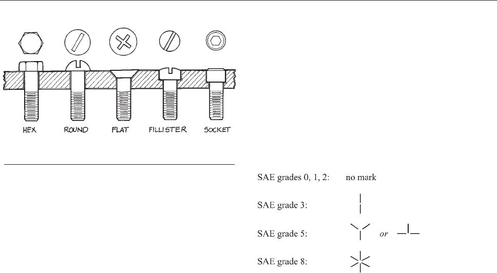
Allen screws. L-shaped, straight, and ball-pointed hex driv-
ers are available that permit Allen screws to be installed in
locations inaccessible to a wrench or screwdriver. An
Allen screw can only be driven by a wrench of the correct
size, so the socket does not wear as fast as the slot in a
slotted-head screw. Socket-head screws have a relatively
small bearing surface under the head and should be used
with a washer where possible.
Setscrews are used to fix one part in relation to another.
They are often used to secure a hub to a shaft. In this
application it is wise to put a flat on the shaft where the
setscrew is to bear; otherwise the screw may mar the shaft,
making it impossible for it to be withdrawn from the hub.
Setscrews should not be used to lock a hub to a hollow
shaft, since the force exerted by the screw will deform the
shaft. In general, setscrews are suitable only for the trans-
mission of small torque, and their use should be avoided if
possible.
Machine screws shorter than 5 cm (2 in.) are threaded
their entire length. Longer screws are only threaded for
part of their length. Screws are usually only available with
class 2A coarse or fine threads.
The type of head on a screw is usually designated by an
abbreviation such as ‘‘HEX HD CP SCR’’ or ‘‘FILL HD
MACH SCR.’’ For example, a socket-head screw 1 1/2 in.
long with an 8–32 thread is designated
832 UNC 1 1=2 SOC HD CAP SCR
The torque T required to produce a tension load F in a
bolt of diameter D is
T ¼ CDF,
where the coefficient C depends upon the state of lubrica-
tion of the threads. In general, C may be taken as 0.2. If
the threads are oiled or coated with molybdenum disulfide,
a value of 0.15 may be more accurate. If the threads are
very clean, C may be as large as 0.4. The tension load on
the bolt is equal to the compressive force exerted by the
underside of the bolt head.
Steel bolts meeting SAE specifications are identified by
markings on the head:
The strength of the bolt increases with the SAE grade
number. Most common steel bolts are SAE grade 2. In sizes
up to 1 in., these bolts have a yield strength of 30 000 to
50 000 psi. The yield strength of SAE grade 5 bolts exceeds
90 000 psi while that of grade 8 bolts exceeds 130 000 psi.
When a bolt is to be tightened to a specified torque, the
threads should be first seated by an initial tightening. It
should then be loosened and retightened to the computed
torque with a torque wrench. The torque corresponding
to the yield strength should not be exceeded during this
operation.
To obtain maximum load-carrying strength, a steel bolt
engaging an internal thread in a steel part should enter the
thread to a distance equal to at least one bolt diameter . For a
steel bolt entering an internal thread in brass or aluminum, the
length of engagement should be closer to two bolt diameters.
Machine screws are readily available in a remarkable
range of materials and finishes. Run-of-the-mill steel
screws are often zinc plated, but nickel- and chrome-plated
screws are available for enhanced corrosion resistance and
better appearance. In addition to steel screws, major
suppliers provide screws and nuts in types 304 and 316
stainless steel, Monel, brass, silicon bronze, 2024-T4 alu-
minum, titanium, Nylon, Teflon, and fiberglass-reinforced
Figure 1.19 Machine screws: hex head; round head
(slotted); flat head (Phillips); fillister head; socket head.
JOINING MATERIALS 27

plastic. The choice of the material for a threaded fastener
depends on the desired strength in the joint to be made, the
materials to be joined, and the environment of the finished
assembly. The possibility of corrosion weakening a joint or
preventing disassembly is often a major factor. Galvanic
action between the materials of the fastener and the joined
assembly is the culprit here. The material of the fastener
and of the metals being joined should be close to one
another in the galvanic series. Metal screws are to be
avoided when joining metals far apart in the galvanic ser-
ies; brazing is preferable in this situation.
As a threaded assembly is tightened, the interlocking
threaded surfaces are held together by the stress created
by elastic deformation of the fastener and the clamped
parts. Shock, vibration, and thermal cycling can relieve
this tension and the assembly becomes loose. All manner
of schemes have been developed to keep threaded parts
locked together. For instrument assembly, lockwashers
often suffice. These come in two forms: the spring lock-
washer and the serrated washer. The former is simply a
washer in the form of a single-turn spring that is placed
under the head of a bolt or under a nut before it is screwed
onto the bolt. The washer is flattened as the assembly is
tightened. The spring force creates friction to resist the bolt
turning. A toothed or serrated washer simultaneously
engaging the surface of the joined part and the underside
of a bolt or nut similarly resists a bolt’s turning loose. As
an aside it is usually noted that a lockwasher should not be
used along with a flat washer since the lockwasher will
engage the flat washer on one side, but the other side of the
flat washer will slip. Self-locking screws are made with a
nylon insert in the threads. The nylon deforms as the screw
is installed to take up the clearance between the mating
threaded surfaces. Nuts with nylon inserts, so-called ‘‘air-
craft nuts,’’ are readily available and quite effective in
resisting loosening under vibration. A simple means of
securing a nut and bolt assembly is to install a second
nut, the locknut, after the first nut is tightened. With the
first nut held securely with a wrench to prevent its turning,
the locknut is tightened down on the first. The effect is to
create opposing tension in the bolt that takes up clearance in
the threads and increases friction between the mating sur-
faces. A threaded assembly can also be secured with adhe-
sive applied to the threads to take up clearances and stick
the surfaces together. Specialized adhesives for this purpose
(Loctite) are available in a range of strengths for both
removable and permanent installations.
Excessive wear may result when a steel bolt is screwed
into a threaded (tapped) hole in a soft material such as
plastic o r aluminum. Threaded inserts (Heli-Coils) can
be installed in the softer material to alleviate this prob-
lem. These inserts are tightly wound helices of stainless
steel or phosphor bronze wire with a diamond-shaped cross
section. The insert is placed in a tapped oversize hole and
the mating bolt is screwed into the insert. Special taps are
required to prepare a hole for the insert, and a special tool
is required to drive the insert into the hole.
1.4.2 Rivets
Rivets are used to join sheet-metal or sheet-plastic parts.
They are frequently used when some degree of flexibility is
desired in a joint, as when joining the ends of a belt to give
a continuous loop. Common rivet shapes are shown in
Figure 1.20. Rivets are made of soft copper, aluminum,
carbon
steel, and stainless steel, as well as plastic. As for
threaded fasteners, the strength required in a joint and the
possibility of corrosion are considered in choosing the
material for a rivet. To join two pieces, a hole, slightly
larger than the body of the rivet, is drilled or punched in
each piece. The holes are aligned and the rivet is inserted.
The length of the rivet should be such that it protrudes a
distance equal to one to one and half times its diameter.
The head of the rivet is backed-up with a heavy tool while
the plain end of the rivet is ‘‘upset’’ by hammering to
draw the two pieces together. The hammering action
swells the body of the rivet to fill the hole. Vise-like hand
tools with appropriate die sets are available for setting
rivets in a one-handed operation.
Blind rivets or ‘‘pop’’ rivets, illustrated in Figure 1.20 ,
ar
e use ful in t he lab. These can be installed without ac cess
to the back side of the joint. An inexpensive blind r ivet
tool is required. The tool grasps a mandrel that passes
through t he center of the rivet, the rivet is i nserted into
the hole, and the rivet tool pulls the mandrel back until it
breaks. The head of the mandrel rolls the stem of the rivet
over to form a head. Some pop rivets are designed so that
the remaining broken portion of the mandrel seals the
center hole of the rivet. The installation of pop rivets in
carefully positioned, reamed holes is an excellent means
28 MECHANICAL DESIGN AND FABRICATION
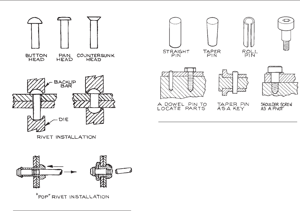
of aligning two thin pieces with respect to one another.
Poprivetedjointscanberegardedassemipermanent.
The rivet is easily removed by drilling into its center with
an oversize drill until the head separates from the body.
With care, the drill will never touch the parts joined by
the rivet.
1.4.3 Pins
Pins such as are shown in Figure 1.21 are used to precisely
locate one part with respect to another or to fix a point of
rotation. To install a pin, the two pieces to be joined are
clamped together and the hole for the pin is drilled and
then reamed to size simultaneously in both pieces.
Straight pins are made of steel that has been ground to a
diameter tolerance of 60.003 mm ( 6.0001 in.). They
require a hole that has been reamed to a close tolerance;
straight pins are to be pressed into place. If a straight pin is
to serve as a pivot or if it is to locate a part that is to be
removable, the hole in the movable part is reamed slightly
oversize.
A roll pin has the advantage of ease of installation and
removal and does not require a precision-reamed hole. The
spring action of the wall of the pin holds it in place.
Taper pins are installed in holes that are shaped with a
special reamer. The American taper is 0.250 in. per ft. The
metric taper is 1:50. Plain taper pins are driven into place.
Taper pins with the small end threaded are drawn into
place with a nut that then secures the installed pin.
A shoulder screw is effectively a straight pin with a
shoulder to provide location and a threaded end below
for attachment. Shoulder screws are used as pivots. These
screws are hardened, and the shoulder is ground to a diam-
eter tolerance of 60.0001 in.
1.4.4 Retaining Rings
A retaining ring (Figure 1.22) serves as a removable shoul-
der to position an assembly of parts on a shaft or in a hole.
An axially assembled external retaining ring is expanded
slightly with a special pair of pliers, then slipped over the
end of a shaft and allowed to spring shut in a groove on the
shaft. An axially assembled internal ring is compressed,
inserted in a hole and permitted to spring open into a
groove. A radially assembled external retaining ring is
Figure 1.21 Pins and shoulder screws.
Figure 1.20 Rivets and riveted joints.
JOINING MATERIALS 29
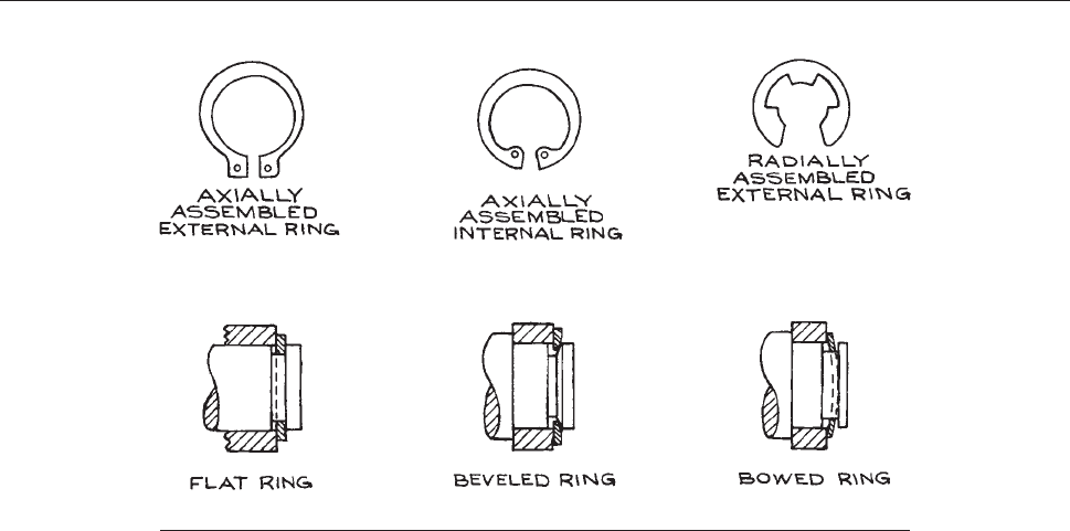
forced onto a shaft from the side. It springs open as it slides
over the diameter and then closes around the shaft. Some
retaining rings have a beveled edge, as shown in the figure.
Spring action of the ring on the edge of its groove produces
an axial load to take up unwanted clearances between
assembled parts. This scheme is frequently used to take
up the end-play in a ball bearing. A bowed retaining ring
provides another solution to end-play take-up. The variety
and range of sizes of retaining rings are truly remarkable.
The Truarc Division of Waldes Kohinoor is a major sup-
plier of retaining rings.
1.4.5 Soldering
In soldering, as well as brazing, two metal surfaces are
joined by an alloy that is applied in the molten state to
the joint. The melting point of the alloy is below that of the
metal of the parts to be joined (the so-called base metal).
Soldering and brazing differ in the composition of the fusi-
ble alloy. Solder is a tin alloy that melts at a relatively low
temperature – in the 200–300 °C range. Brazing was orig-
inally done with a copper alloy that melts at about 900 °C.
There are now many different brazing alloys with working
temperatures from 400 °C to more than 2000 °C. Today the
term ‘‘brazing’’ usually implies ‘‘silver brazing’’ with silver-
containing alloys that flow in the 450–800 ° C range.
The molten soldering or brazing alloy must wet the
surfaces of the metal parts being joined. When the alloy
wets the surfaces of closely spaced parts, capillary action
draws the alloy into the joint to provide the largest possible
contact area and correspondingly the strongest possible
joint. A dirty or oxidized metal surface will not be wetted.
A chemically-active flux is applied as the base metal is
heated to remove oxides and protect the surface thus
cleansed. The flux employed is, to a certain extent, specific
to the base metal and the alloy as well as the temperature
required for melting the solder or braze alloy.
For routine soldering of copper or brass parts, 50–50
tin–lead solder (50% tin, 50% lead) has traditionally been
the alloy of choice. Lead-containing solder is no longer
used for piping in contact with potable water. Tin–lead
solder has being replaced by 95–5 tin–antimony for joining
copper to copper. The 96–4 tin–silver eutectic (96.5% tin,
3.5% silver) has melting and flow properties similar to
tin–lead solder and, with the use of the proper flux, will
wet copper, brass, steel, and stainless steel. 60–40 tin–lead
solder is used to join electronic components. Soldered
joints are appropriate when great strength and cleanliness
are not required and when it is most convenient to work at
Figure 1.22 Retaining rings and retaining ring installations.
30 MECHANICAL DESIGN AND FABRICATION

low temperatures. The tensile strength of a copper sleeve
joint with tin–lead solder is about 40 MN/m
2
(6000 psi).
The shear strength is about 35 MN/m
2
(5000 psi). The
strength of a tin–lead joint is considerably reduced at tem-
peratures above 100 °C.
Steel and stainless steel, as well as brass and copper, can
be soldered with tin–silver alloy solders. The 96–4 tin–
silver eutectic alloy is almost universally applicable in the
laboratory for low-temperature soldering. It melts at 221 °C
and can produce a joint with a tensile strength of 100 MN/
m
2
(15 000 psi) and a shear strength of 75 MN/m
2
(11 000
psi). The manufacturers of soldering and brazing alloys
(including Engelhard, Handy & Harman/Lucas–Milhaupt,
Harris Products, Wesgo Metals, CWB Ltd.) provide tin–
silver alloy solders in wire form, in wire with a rosin flux
core for electronic applications, and as a paste or slurry of
alloy powder in a liquid flux. The last is simply painted on
the surface where desired and heated indirectly. The
absence of flux on adjoining areas keeps solder from flow-
ing where it is not wanted.
Soldering alloys containing lead, zinc, antimony, or cad-
mium should be avoided. These components are volatile.
Zinc is sufficiently volatile at room temperature to be a
significant contaminate in high-vacuum applications. Cad-
mium vapor at soldering temperatures is a serious health
hazard.
The first step in soldering a joint is to clean the surfaces
to be joined with fine emery paper or steel wool. The sur-
faces are then covered with soldering flux, assembled,
and heated. A gap of 0.1–0.2 mm (.003–.006 in.) is desir-
able between surfaces to be soldered. In some cases it may
be necessary to insert a piece of brass shim stock to main-
tain this clearance. When heated, the flux removes oxides to
cleanse the surfaces so the molten solder will wet them. Sal
ammoniac (NH
4
Cl) flux, available from hardware suppli-
ers, is used for lead–tin solders. The suppliers of lead-free
solders provide proprietary fluxes. A natural-gas–air flame
or propane–air flame is most convenient. The assembly may
also be heated on an electric or gas hot plate. Flame heating
should be done indirectly if possible. Play the flame on the
metal near the joint, particularly on the heavier of the two
pieces. Periodically test the temperature of the two pieces
by touching each with the solder. When each piece is hot
enough to melt the solder, remove the flame and apply
solder to the joint. The solder should flow by capillary
action into and through the joint. Sufficient solder should
be applied to fill the joint and produce a meniscus or fillet of
solder at the juncture of the two parts (Figure 1.23). The
fi
llet radius should be 1/16–1/8 in. Residual flux must be
removed. This is why it is important that the joint is filled
with molten solder. Flux trapped in the joint will lead to
hidden corrosion. Inorganic flux can be dissolved in hot
water. Organic fluxes will require an organic solvent.
1.4.6 Brazing
A brazed joint is strong and leak tight. The brazing process
is amenable to the laboratory and the simplest shop. A
brazed assembly can offer real advantages to the designer
of an apparatus. Surprisingly often, a complex part can be
inexpensively made by brazing together an assembly of
standard off-the-shelf parts. Brazing offers a relatively
easy means of joining materials with very different proper-
ties: a hard metal can be joined to a flexible metal stem;
a metal with desirable electrical and thermal properties
can be incorporated in an assembly made of a metal with
entirely different properties; a strong metal-to-ceramic
brazed joint is possible.
There a re hundreds of brazing alloys.
5
The choice of an
alloy depends upon t he metals to be joined and the appli-
cation of the brazed part. The strength of the alloy in a
joint is seldom an issue in a properly designed joint. I n
some instances the joint strength will exceed that of the
base metal. The wetting and flow characteristics of the
molten brazing alloy are often of primary importance. Of
course the working temperature of the brazing alloy must
be l ess than the melting poi nt of the base metal, some-
times, much less, to avoid an undesirable phase transition
in the base metal.
Alloys are characterized by a solidus, the temperature
at which, upon heating, liquid mixed with solid first
Figure 1.23 A soldered joint.
JOINING MATERIALS 31

appears, and a liquidus, the temperature at which the alloy
becomes completely liquid. The difference between the
two temperatures is the melting range. In brazing a joint,
an alloy with a narrow melting range (0–20 °C) becomes
fluid quickly and will tend to flow into the narrowest gap.
For a joint with relatively large gap (greater than about 0.1
mm), a large melting range is desired so that upon heating,
the alloy remains in the melting range and flows sluggishly
to fill the joint. A eutectic alloy melts at a single temper-
ature; there is no melting range.
For routine brazing of steel parts, borate-flux-coated,
brass brazing rod is available from hardware suppliers as
well as specialized suppliers of brazing and welding mate-
rials. The tensile strength of joints made with brass brazing
alloy can be of the order of 50 000 psi. An oxyacetylene
torch is required for brass brazing alloys.
Silver brazing alloys are preferred for most laboratory
work. Silver alloys are lower-melting than brass alloys and
can be used on brass as well as steel parts. The tensile
strength, as well as the shear strength, of silver-brazed
joints is in the 200–350 MN m
2
(30 000–50 000 psi)
range, depending upon the alloy and the joint design.
The alloy of approximately 60% silver, 30% copper, and
10% tin is generally applicable. It melts at 600 °C (solidus)
and flows at 720 °C (liquidus), and can be worked with the
same gas-oxygen torch used for laboratory glassblowing.
A fluoride flux is required. Parts made of copper, brass,
steel, stainless steel, and even refractory metals can be
joined with this brazing alloy.
When volatile metals cannot be tolerated, the silver–
copper eutectic (72% Ag, 28% Cu) makes a suitable braz-
ing alloy for copper, stainless steel, Kovar, and many
refractory metals. This alloy melts at 780 °C. For torch
brazing, an oxyacetylene flame is required. The addition
of indium produces a lower-melting alloy with much the
same properties as the silver–copper eutectic. Incusil-15
(62% Ag, 24% Cu, 15% In, Wesgo), for example, has a
solidus of 630 °C and a liquidus of 705 °C. Silver-bearing
brazing alloys containing cadmium or other volatile metals
should be avoided. Cadmium vapor is toxic. Volatile com-
ponents (i.e., zinc) of a brazing alloy can cause significant
contamination in a high-vacuum system.
The manufacturers (including Handy & Harman/Lucas–
Milhaupt, Engelhard, Harris Products, Wesgo, Aufhauser,
CWB Ltd.) provide alloys for a remarkable range of
applications along with the fluxes appropriate for each
alloy–base metal combination. Brazing alloys are offered
in rod or wire form, as either flux-coated or flux-cored rod,
and as a paste incorporating powdered alloy and flux.
Torch brazing is the simplest and most convenient braz-
ing operation. An oxyacetylene torch is required for brass
brazing alloys. A natural-gas–oxygen flame can be used
for lower-melting alloys. The flame must be nonoxidizing.
The flame should be adjusted to provide a well-defined,
blue, inner cone 8–10 mm long. The oxyacetylene flame
should have a greenish feather at the tip of the inner cone.
A fireproof working surface is also required. Most fluxes
contain sodium, which emits yellow light when heated. A
pair of didymium eyeglasses, such as are used in glass-
blowing, will filter out the sodium yellow lines and make
the work much more visible while brazing. Parts to be
brazed should, if possible, be designed to be self-locating.
A clearance between parts of 0.03–0.1 mm (.001–.003 in.)
will assure maximum strength in the finished joint. Surfa-
ces to be wetted by the brazing alloy must be clean.
The brazing process is not unlike the soldering process
described above. Coat the joint surfaces with flux and
assemble the parts. Clamp if necessary: parts move as a
consequence of differential expansion as they are heated;
the blast of gas from a torch can misalign an assembly.
Preheat the base metals in the area of the joint nearly to
the melting temperature of the brazing alloy. The flux
should melt from its crystalline form to a glassy fluid as
the brazing temperature is approached. Continue heating
while testing both pieces to be joined by touching the base
metal with the brazing rod. The rod should melt in contact
with both pieces. Do not apply the flame directly to the
brazing rod. When the brazing alloy flows, continue to heat
the entire area of the joint. There are two dangers: insuffi-
cient heat and too localized heating. The molten alloy flows
toward the hottest area of the joint; a void may be left in a
cool area to weaken the joint. Intense localized heating will
consume flux and leave the base metal exposed to oxidation
that will prevent further wetting by the molten alloy, once
again leaving a weak place in the joint. Overheating also
mars the finish of the metal. In general, make sure there is
adequate flux and that the quantity of alloy is sufficient to fill
the joint and leave a fillet at the juncture of the parts being
joined. It is sometimes convenient to preplace snippets of
brazing wire in or near the joint before heating, rather than
32 MECHANICAL DESIGN AND FABRICATION

applying the alloy after the work is heated. Alloy/flux pastes
provide another effective means for assuring that the alloy is
effectively introduced in a joint. Finally it is essential that
corrosive flux residues be removed from the finished joint.
One of the easiest approaches is to quench the brazed part in
water before it is completely cool. The thermal shock frac-
tures the glassy residue which then dissolves in the hot
water. Be careful here: the thermal shock may also distort
thin sections in the part being brazed. A wire brush and
emery cloth may be used to finish the job. A rinse in an
acid solution may be necessary if the part has been over-
heated to the extent that the base metal has been oxidized.
Many metals, as well as brazing fluxes and alloys, con-
tain toxic components that are volatile at brazing temper-
atures. Brazing should be carried out in a well-ventilated
hood. Cadmium-containing brazing alloys should not be
used in the laboratory. One should be aware that many
standard parts are plated with cadmium or zinc. The
plating must be removed before heating to brazing
temperatures.
Copper, Kovar, Monel, nickel, steel, and stainless steel
can be brazed without flux if the metal is heated in a hydro-
gen atmosphere in a furnace. The hydrogen serves as a flux
by reducing surface oxides to produce a clean surface that
will be wetted by the molten brazing alloy. Alloys contain-
ing chromium must be brazed in dry hydrogen. The surface
oxide of chromium found on stainless steel is reduced by
dry hydrogen at temperatures above 1050 °C. Furnace
brazing provides for more uniform heating of the work
so there is usually less distortion than in torch brazing.
The work is also stress-relieved to some extent. Hydro-
gen-brazed parts come out clean and bright. Although it
is possible to carry out hydrogen brazing in the lab, the job
is better let out to a specialty shop. Commercial heat-treat-
ing shops operate dissociated-ammonia tunnel kilns. The
work travels slowly through the kiln on a car. Ammonia
introduced in the middle of the furnace dissociates to
hydrogen and nitrogen to provide the flux.
Parts to be hydrogen-brazed should be chemically clean.
Avoid fingerprints, since inorganic salts from the skin are
not affected by hydrogen and will remain as stains on the
finished work. Assemble the parts and place snippets of
filler-metal wire at the junction of the parts to be brazed.
For parts that are not securely self-aligned it may be worth-
while to pin the joints to maintain precise alignment. A
rough calculation of the volume to be filled will determine
the amount of wire to be used. When the filler metal melts,
it is drawn into the nearby joint by capillary action. If the
joints to be brazed are not visible from outside the furnace,
place a piece of brazing metal on top of the work where it
can be observed by the operator, in order to determine
when the brazing temperature has been reached. If the
walls of the brazing apparatus are opaque, a thermocouple
will be required for this purpose.
The filler metal used in hydrogen brazing should melt at
a temperature higher than that required for the hydrogen to
effectively clean the surface of the base metal. OFHC
(oxygen-free high-conductivity) copper has a melting
point of 1083 °C and is an excellent filler metal for brazing
steel, stainless steel, Kovar, and nickel. If low-melting
alloys, such as the silver–copper eutectic, are used, a small
amount of flux is required. Brazing alloys that contain
volatile metals should never be used for hydrogen brazing.
It is unwise to braze parts of ordinary electrolytic copper or
to use ordinary copper as a filler in a hydrogen atmosphere.
Oxides in the metal are reduced to water that is trapped
within the crystalline structure of the metal. This water can
cause out-gassing problems in vacuum applications, and, if
the copper is heated, the expanding water vapor will pro-
duce internal cracks (hydrogen embrittlement). For instru-
ment work, OFHC copper should be used for all copper
parts that are to be brazed.
A brazed joint between ceramic pieces or between metal
and ceramic is entirely possible although the operation
must be carried out in a vacuum furnace or in a furnace
under an inert atmosphere. Appropriate filler metal–flux
pastes are used (for example, Lucanex from Lucas–
Milhaupt). One must take into account the difference in
thermal expansion of the parts to be joined. Refractory
metals, such as molybdenum, tantalum, or tungsten, have
coefficients of thermal expansion close to those of most
ceramics. Ferrous and cuprous alloys can be brazed to
ceramic materials if the metal part is thin in the region
of the joint to allow for some give in the metal part as it
cools down from the brazing temperature.
1.4.7 Welding
In welding, parts are fused together by heating above the
melting temperature of the base metal. Sometimes a filler
JOINING MATERIALS 33

metal of the same type as the base metal is used. Fusion
temperatures are attained with a torch, with an electric arc,
or by ohmic heating at a point of electrical contact. For
most instrument work the preferred method is arc welding
under an argon atmosphere using a nonconsumable elec-
trode. This method is referred to as tungsten-inert-gas
(TIG) welding or heliarc welding. All metals can be
welded, although refractory metals must be welded under
an atmosphere that is completely free of oxygen. Arc weld-
ing requires special skills and equipment, but most instru-
ment shops are prepared to do TIG welding of steel,
stainless steel, and aluminum on a routine basis.
The effect of the high temperatures involved must be
considered when specifying a welded joint. Some distor-
tion of welded parts is inevitable. Provision should be
made for remachining critical surfaces after welding.
The state of heat treatment of the base metal is affected
by welding. Hardened steels will be softened in the vicinity
of a weld. Stainless steels may corrode because of carbide
precipitation at a welded joint.
Spot welding or resistance welding is a good technique
for joining metal sheets or wires in the lab. The joint is
heated by the brief passage of a large electric current
through a spot contact between the pieces to be joined.
Steel, nickel, and Kovar, as well as refractory metals such
as tungsten and molybdenum, can be spot-welded. Copper
and the precious metals are not easily spot-welded because
their electrical resistance is so low that very little power
can be dissipated at the point of contact. Small spot-
welding units with hand-held electrodes are available
from commercial sources (Ewald Instruments, Miyachi
Unitek, PUK).
1.4.8 Adhesives
Epoxy resins are the most universally applicable adhesives
for the laboratory. They are available in a variety of
strengths and hardnesses. Epoxies that are either thermally
or electrically conducting are also available. Epoxy adhe-
sives consist of a resin and a hardener that are mixed just
prior to use. The mixing proportions and curing schedule
must be controlled to achieve the desired properties. A
variety of epoxy adhesives is available prepackaged in
small quantities in the correct proportions. Epoxies will
adhere to metals, glass, and some plastics. Hard, smooth
surfaces should be roughened prior to the application of
the adhesive. Sandblasting is a convenient method. Parts of
a surface that are not to receive the adhesive can be masked
with tape during this operation. To obtain maximum
strength in an epoxied joint, the gap filled by the epoxy
should be 0.05–0.2 mm (.002–.006 in.) wide. To maintain
this gap between flat smooth surfaces, shims can be
inserted to hold them apart.
Self-curing silicone rubber such as General Electric
RTV (Room Temperature Vulcanizing) can be used as an
adhesive. RTV is chemically stable and will stick to most
surfaces. The cured rubber is not mechanically strong; this
can be an advantage when making a joint that may occa-
sionally have to be broken.
Cyanoacrylate contact adhesives, so-called ‘‘super
glues,’’ have found wide use in instrument construction.
Eastman 910 and Techni-Tool Permabond are representa-
tive of this type of adhesive. These adhesives are mono-
mers that polymerize rapidly when pressed into a thin film
between two surfaces. They will adhere to most materials,
including metal, rubber, and nylon. Cyanoacrylate adhe-
sives are not void-filling and only work to bond surfaces
where contours are well matched. An adhesive film of about
0.03 mm (0.001 in.) gives best results. A firm set is achieved
in about a minute, and maximum strength is usually reached
within a day. When joining metals and plastics, a shear
strength in excess of 7 MN/m
2
(1000 psi) is possible.
Ceramic cements are available for a remarkable range of
applications (Sauereisen, Dylon). These are inorganic mate-
rials (silica, zirconia, graphite) in powder, paste, or liquid
form that are used to join ceramics, graphite, and metals.
Some are intended to make electrically insulating coatings;
others may be used for casting small ceramic parts. The
tensile strength of these materials is generally not great,
but the materials are serviceable up to 1100 °C and higher
(much higher in the case of graphite cements).
1.4.9 Design of Joints
The design of the joints between parts of a machine deserves
special attention. Experience indicates that failure of an
assembly frequently occurs at or near a joint. A well-
designed joint must suit the designer’s purposes while at
the same time assuring that there will not be an undesirable
concentration of stress in the vicinity of the joint.
34 MECHANICAL DESIGN AND FABRICATION
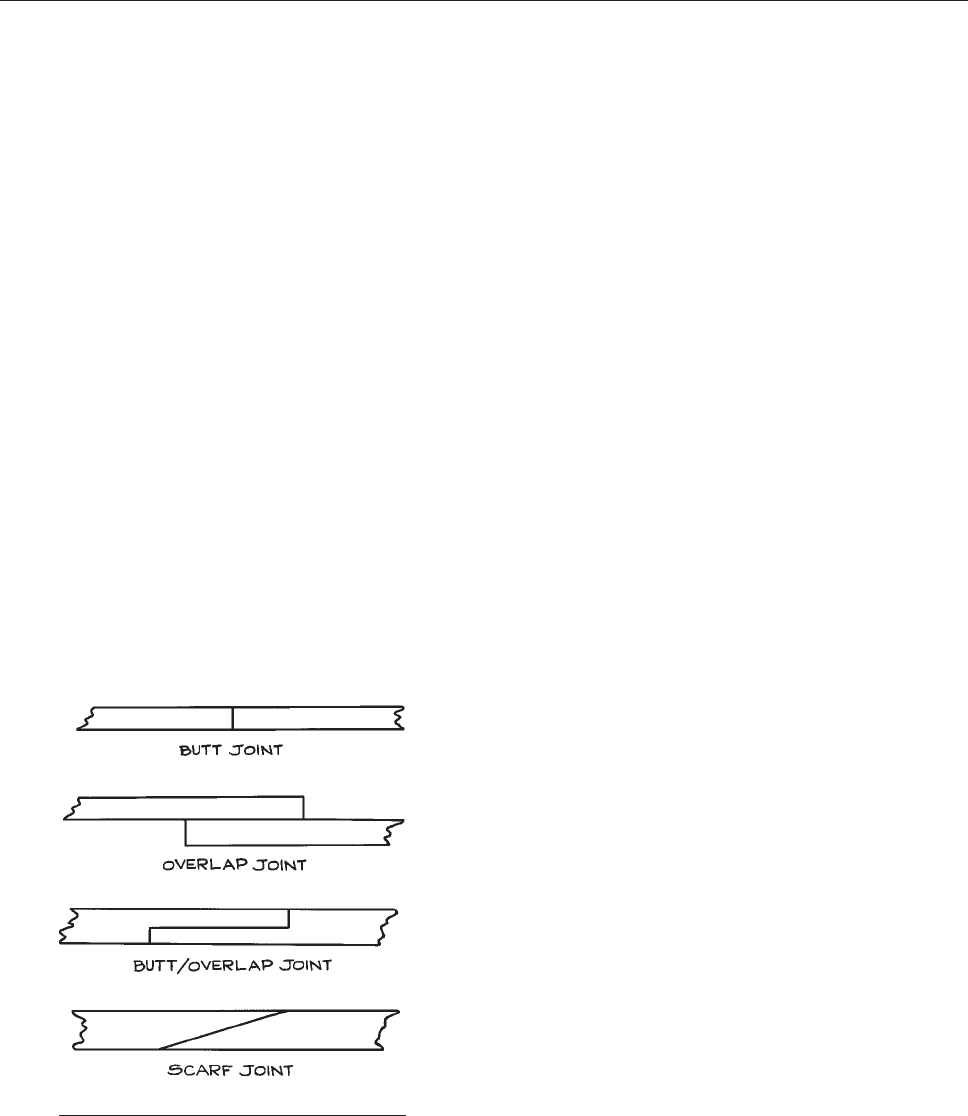
The basic idea is to design the joint so that the assembly
allows for a smooth flow of tensile, bending, and torsional
forces through the joint. One may not intend to stress an
assembly to the point that noticeable distortion occurs, but
imagine that one has done just that: does the strain appear
as a smooth bend or flex or does the strained part have a
‘‘kink’’ in the vicinity of a joint?
There are two types of joints, the butt joint and the
overlap joint, as shown in Figure 1.24 . A butt joint permits
parts
to be joined without an increase in thickness. The
same advantage is realized with a hybrid butt/overlap joint,
at the expense of additional machining and fitting. The
woodworker’s or shipwright’s scarf joint is an example
of a butt/overlap joint.
A joint should be as strong as the parts leading up to the
joint in order to avoid an un desirable stress concentration.
It follows that a butt joint is only amenable to welding.
The contact area in a butt joint is usually too small for a
brazed or soldered joint to provide the strength o f the
adjoining parts. For thin parts butted together, a full-
penetration weld should be specified. (Imagine two thin
pieces of steel butt-welded with only pa rtial weld pene-
tration. If the assembly were flexed it would hinge and
kink at the weld.)
An overlap joint can be soldered, brazed, or glued, pro-
vided the contact area is sufficient to attain the desired
strength. The stronger the material being joined, the longer
must be the overlap so that the joint strength is commen-
surate with the strength of the material.
The butt/overlap joint is amenable to joining with braze,
solder, glue, or rivets. The advantage of a constant cross-
section is lost if the joint is bolted, unless the material
being joined is sufficiently thick that a recessed-head
design is possible.
The designer must decide how permanent a joint is to
be. A brazed, soldered, or welded joint is ordinarily quite
permanent. Reheating, however, can easily disassemble a
soldered electrical connection. Similarly, wires and thin
metal parts that have been lightly spot-welded together
can be broken apart at the weld without damaging the
components. Spot-welding is a useful means for making
electrical connections between refractory-metal parts and
between parts to be used in a high-temperature environ-
ment. A glued joint may be permanent, but, if a soft adhe-
sive such as self-curing silicone is used, the joint can be
disassembled, although not conveniently. A riveted joint
can be disassembled if required and, of course, a bolted
joint can be assembled and disassembled repeatedly. A
force fit permits parts to be assembled in precise alignment
and without fasteners. A force fit usually involves inserting
a round piece into a round hole. The inner piece is
made larger than the hole so that the parts interfere upon
assembly. The parts are permanently or semipermanently
assembled depending on the extent of interference. The
parts must be made with great precision to achieve the
desired result. Mechanical design and drafting books
provide tables of fits. A ‘‘light force fit’’ of parts that can
be disassembled with a press or pin driver requires an
interference of approximately 0.01 to 0.03 mm (.0005 to
.001 in.) in parts up to 5 cm (2 in.) in diameter. Interference
two to three times greater requires a heavy press or heating
to expand the outer part (or cooling to contract the inner
part) to be assembled. Immersion of a part into liquid
nitrogen before it is placed into a hole can lead to a very
strong force fit. Heavy force fits or ‘‘shrink fits’’ are effec-
tively permanent.
It is sometimes desirable to allow for some ‘‘give’’ in a
joint. For example, there is much to be said in favor of
rivets being used to join soft materials such as plastics or
fabric. A riveted lap joint in this case will allow for some
movement between the parts when a stress is applied. This
Figure 1.24 Joints.
JOINING MATERIALS 35
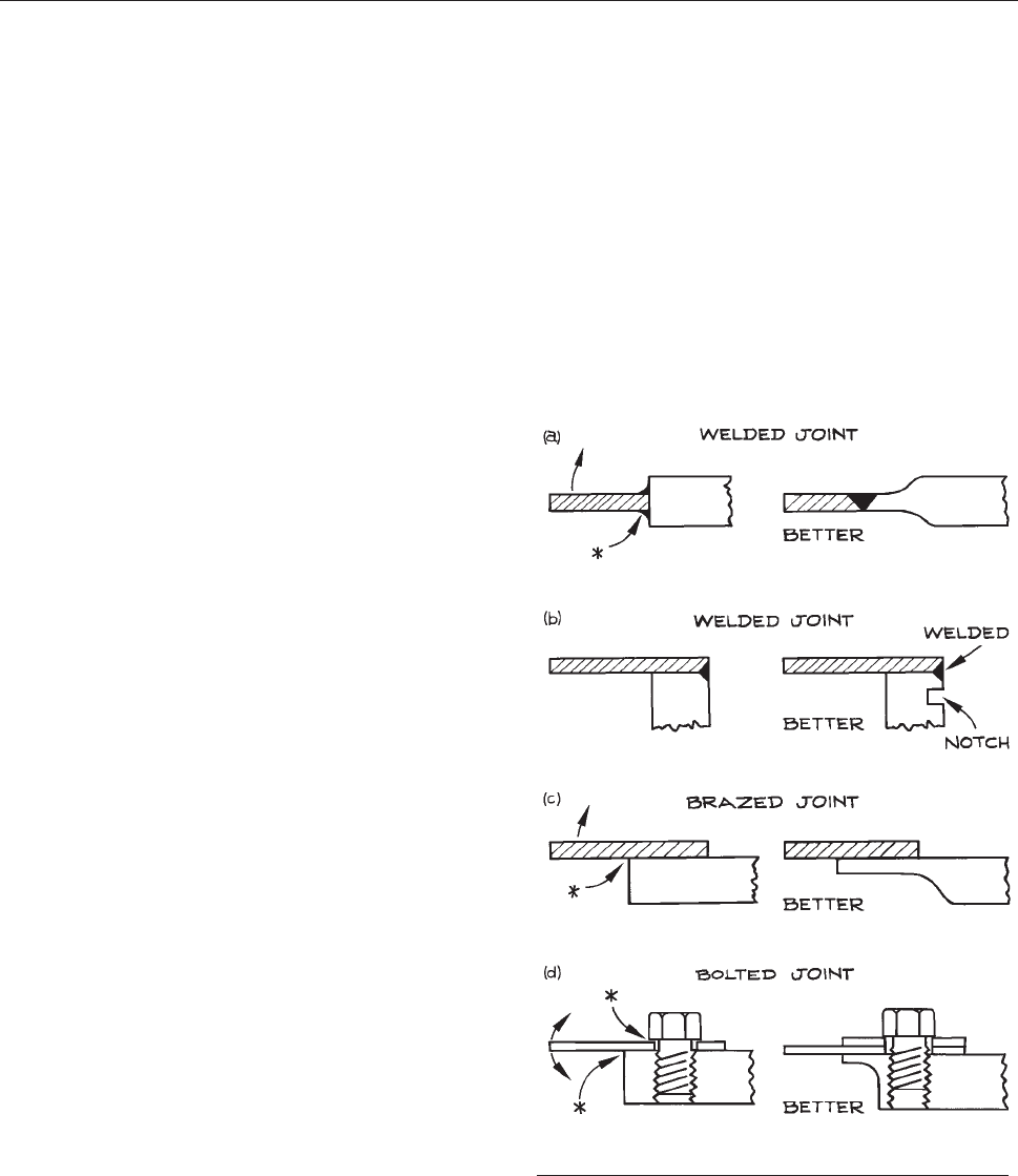
helps relieve stress concentration at the location of the
rivets. As another example, consider a situation where it
is anticipated that joined parts will change their relative
position or shape in response to a sudden temperature
change or differential. A springy fastener such as a bowed
retaining ring may be called for.
As a general rule, a joint should be designed so that the
pieces being joined are of roughly equal strength at the
point where they are joined, as suggested in Figure 1.25.
F
or parts of the same material, this implies that the parts
have the same cross-section at the joint or the same thick-
ness if the parts are of the same width. This is important in
the design of welded and brazed joints for reasons of both
manufacturer and application. Welding (as well as brazing)
parts of different thicknesses risks a weak joint because of
the differential in the rate of heat loss through the parts
being joined. The thinner part is overheated or the thicker
part does not achieve the temperature needed for fusion to
the proper depth (or, in the case of brazing, to be properly
wetted). The resulting state of heat treatment may be dif-
ferent on one side from the other. This will create a stress
riser since one side may be more flexible than the other. In
general, the dimension of weld penetration should be the
same as the thickness of the parts near the joint. When a
thick piece of metal must be welded to a thin piece, it is
common practice to cut a groove in the thick piece, near
the joint, to limit the rate of heat loss into the heavier piece,
to effectively equalize the dimensions of the weld and the
parts at the location of the weld, and to avoid a concen-
tration of stress at the joint [Figure 1.25(b)]. This situation
arises
when welding a thin tube into a heavy flange (Sec-
tion
3.6.3 and Figure 3.39).
Jo
ints with discrete fasteners such as bolts or rivets have
unique problems. Flexing of the assembled parts may lead
to a stress concentration at the corners of the head of the bolt
or rivet, as suggested in Figure 1.25(d). The designer must
a
lso allow adequate clearance for manufacture and assem-
bly. A tapped hole must leave the machinist clear access
with a drill and tap. For assembly there must be sufficient
clearance to insert a bolt or screw, as well as space for the
wrench or screwdriver used to tighten the fastener. A rivet
hole requires access for a drill and reamer as well as clear-
ance for the tools employed to set the rivet. A threaded hole
that does not pass clear through a part, that is, a ‘‘blind
hole,’’ is sometimes necessary but should be avoided if
possible. A blind hole is difficult to keep clean and free of
debris that will bind the threaded parts when they are being
assembled. There is also the possibility of damage should a
bolt longer than specified be driven into the bottom of a
blind hole. (The author once spent two weeks looking for
a vacuum leak through a crack at the bottom of a blind hole
created by an overlong bolt’s being driven into the bottom.)
The strength of a brazed or soldered overlap joint
depends upon the length of the lap and the shear strength
of the filler metal. An oft-cited rule of thumb for a brazed
joint suggests that the length of the lap should be at least
three times the thickness of the thinner of two pieces being
joined. More precisely, The Brazing Book,
6
[also published
Figure 1.25 A joint should be designed so that the joined
parts are equally strong at the joint.
36 MECHANICAL DESIGN AND FABRICATION

online by Handy and Harman (www.handyharmancanada.
com)], specifies the length of overlap in a brazed joint as
‘ ¼
S
u
t
KS
s
,
where S
u
is the tensile strength of the weaker of the two
parts being joined, t is the thickness of that part, S
s
is the
shear strength of the filler metal, and K is a ‘‘joint integrity
factor’’ to account for how effectively the filler metal has
penetrated the joint and wetted the surfaces being joined (a
value of about 0.8 is typical). Note that the overlap must
increase when joining high-strength materials.
The space between brazed and soldered parts has a sig-
nificant effect upon the strength of the joint. A brazed joint
between parts spaced 0.03 to 0.10 mm (.001 to .003 in.)
apart can be stronger than the base metal. The clearance
between ‘‘slip-fitted’’ machined parts is usually adequate,
although, for parts of materials of very different coeffi-
cients of thermal expansion, one must consider the clear-
ance at the brazing temperature. Shims may be necessary
to keep polished surfaces apart. A blind joint is undesir-
able. The filler metal entering a joint must displace the
flux. Residual flux trapped in a joint will lead to corrosion.
Additionally, visual inspection is required to assure that
the filler metal has flowed completely through a joint.
If a blind joint is unavoidable, vent holes should be pro-
vided for flux escape and inspection into the deepest part
of the joint.
In general, parts to be joined should be designed to be
self-aligning when clamped together. If this is not possible,
or if very precise alignment is required, parts can be pinned
together. The parts are assembled and clamped in the
proper position, small holes are drilled and reamed, and
pins inserted to maintain alignment while the joints are
brazed, welded, or glued.
Special consideration must be given to a joint between
parts made of dissimilar metals. Two important issues are
the differential in the rates of thermal expansion of the
joined parts and electrical currents produced at the point
of contact. Welds between dissimilar metals may crack as
the parts cool or develop cracks when exposed to large
temperature swings. Brazed joints between dissimilar met-
als may be more tolerant of changes in temperature, but
electrolytic corrosion can be a problem. If a brazed joint is
contemplated, a brazing alloy more noble than the base
metals should be used. If electrolytic effects are a problem,
one solution may be to interpose an insulating layer
between the parts being joined. A layer of paint will suffice
provided that the parts are secured in such a way that
relative movement between the parts does not abrade the
insulating layer. In a wet environment, avoid threaded con-
nections between dissimilar metals; corrosion will occur at
the threads where they are hidden from inspection.
1.4.10 Joints in Piping and Pressure
Vessels
Safety is the primary consideration in specifying or design-
ing a joint in a pressurized conduit or vessel. At high
pressures a sudden failure in a joint threatens life and limb.
At lower pressures a ruptured joint can result in expensive
damage if not personal injury. Of course, having consid-
ered safety in the design of a joint, the next requirement is
that the joint not leak. Short of personal injury, there is
perhaps no worse lab disaster than to spring a water leak
late Friday after everyone has gone home for the weekend.
It is generally desirable that a pressure vessel be built up
of cylindrical sections: the design and analysis of a cylindri-
cal vessel is easiest and most reliable (see Section 1.6.3);
joints
between concentric cylindrical sections are most easily
manufactured and assembled. Joints in the side of a cylin-
drical section are to be avoided: the design of such a joint is
diffi cult at best, the joint is a stress riser , and the fabrication
is inevitably diffi cult and expensiv e. In any event, a joint in a
pressure vessel must be as strong as the joined parts.
A joint in a pressure vessel may be demountable or
permanent depending on the particular requirements. A
demountable joint requires a compressible element of
rubber or metal – a gasket – that is trapped between more
robust surfaces at the joint. This element is elastically
deformed to provide the force required for sealing.
A permanent, leak-proof joint can be welded, brazed, sol-
dered, or glued depending on the pressure in the fluid being
contained. A pipe-threaded joint may be demountable, but
often inconveniently so.
Pipes and pipe fittings are threaded together. Pipe threads
are tapered so that a seal is formed when an externally
threaded pipe is screwed into an internally threaded fitting.
The American Standard Pipe Thread, designated NPT for
National Pipe Thread, has a taper of 1 in 16. The diameter of
JOINING MATERIALS 37
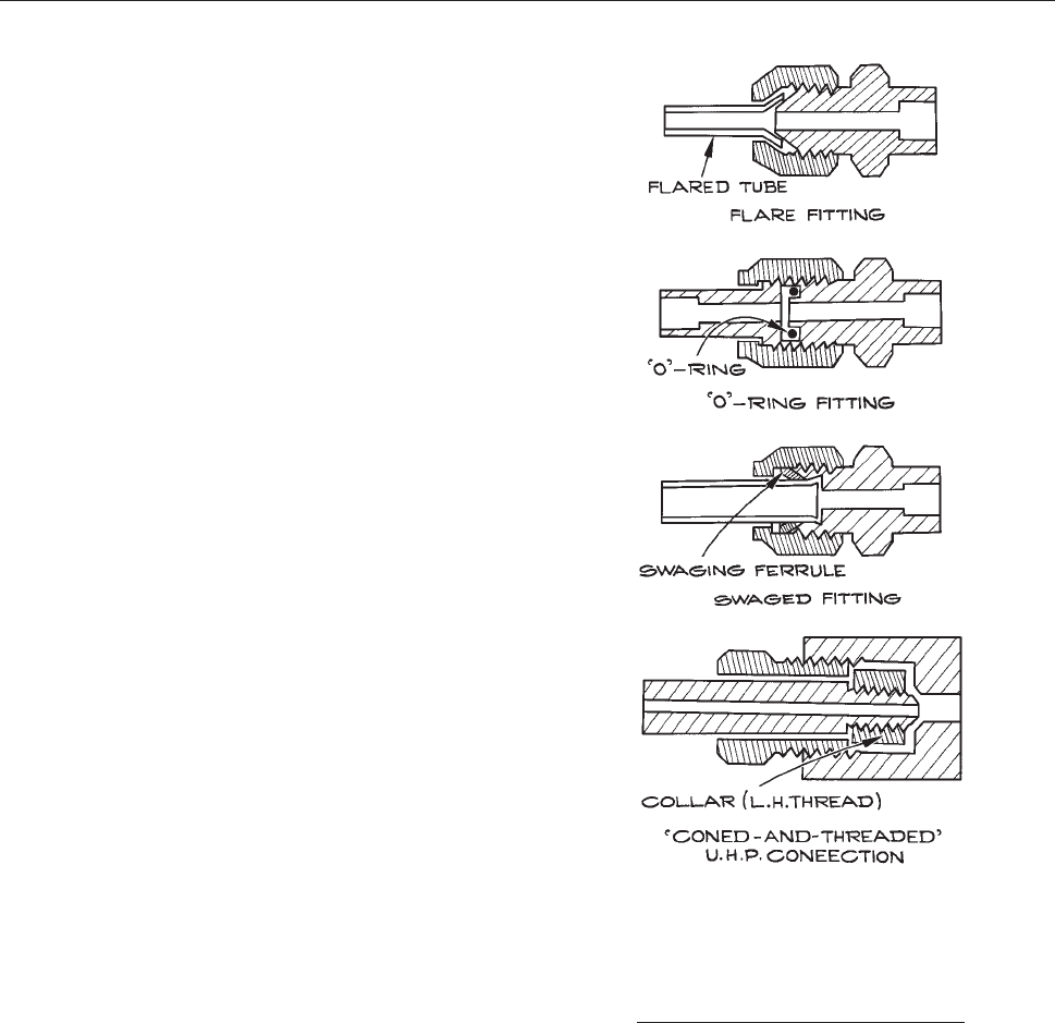
a pipe thread is specified by stating the nominal internal
diameter of a pipe that will accept that thread on its outside.
For example, a pipe with a nominal internal diameter of
1/4 in. and a standard thread of 18 tpi is designated
1=418 NPT
or simply
1=4NPT:
The American Standard Pipe Thread specifications are
listed in Appendix 1.4.
In
Britain and Europe the usual tapered pipe thread
specification is the British Standard Pipe Thread Tapered
(BSPT, BS EN 10226 equivalent to ISO 7). The taper is 1
in 16 and the size is given as the nominal bore of a pipe
with an external thread. The specifications for the British
Standard Pipe Thread Tapered are given in Appendix 1.5.
One
should take care not to confuse tapered pipe threads
(ISO 7) with the British Standard Pipe thread Parallel (ISO
228). The latter are not intended to make a leak-tight joint.
Demountable pressure fittings are illustrated in
Figure 1.26. These include joints where the tubing itself
i
sflaredorswagedtomakeoneelementofthejoint,
joints where the seal is effected by a rubber O-ring or
soft metal gasket, and ultrahigh-pressure joints, in which
a c onical surface machined on the end of thick-wall tub-
ing is driven against a conical receptacle by a threaded
assembly (a so-called ‘‘coned-and-threaded’’ joint). The
last are commonly found in the laboratory as connections
to gas cylinders an d pressure regulators. T he configura-
tion of cone and thread are specific to each gas. These
connections have been stand ardiz ed by the Compressed
Gas Association and are identified by a ‘‘CGA’’ number.
The mechanical configurations of thirty three CGA fit-
tings are given in Ap pend ix 1.6. Note that some of these
fi
ttings have a left-hand thread to prevent mixing of fit-
tings for incompati ble gases. For all mechanical fittings it
is important to foll ow the manufacturer’s instructions for
assembly (this is especially important for the assembly of
flare and swage fittings, where precise deformation of the
tubing is essential to a leak-proof seal). Pay attention a s
well to the manufacturer’s specification of pressure lim-
its, bearing in mind that the pressure limitation for each
type of connection is likely todecreasewithanincrease
in the diameter of the tubing.
The commercial market offers a remarkable number of
inexpensive assemblies that employ standard demountable
joints. These include tees, crosses, Ys, reducers, valves, and
pumps in sizes from a few millimeters to at least 20 cm in
Figure 1.26 Demountable joints for
tubing: (a) a flare fitting, (b) an ‘‘O’’-ring
gasketed joint (Swagelok
Ò
VCO),
(c) a swaged fitting (Swagelok
Ò
),
(d) a ‘‘coned-and-threaded’’
ultrahigh-pressure connection.
38 MECHANICAL DESIGN AND FABRICATION
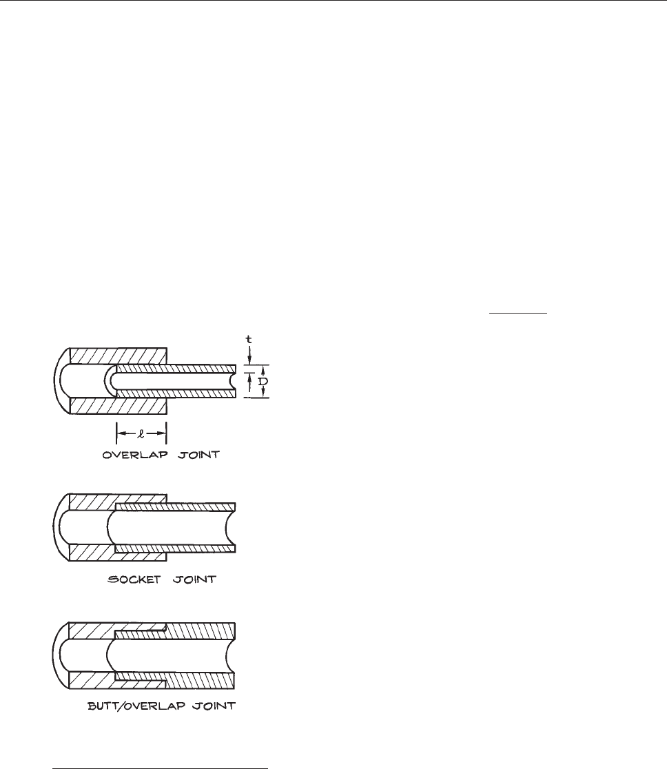
brass, steel, and stainless steel. These assemblies may be
intended for the dairy, automotive, or hydraulic equipment
industries, but can serve well in the lab. An entire apparatus
can be assembled from readily available standard assem-
blies at significant savings in money and time. An hour’s
research on the web can save reinventing the wheel.
Permanent joints in piping and pressure vessels are
typically soldered or brazed cylindrical overlap joints, or
welded cylindrical butt joints.
Roughly speaking and assuming the ratio of diameter (D)
to wall thickness (t) does not exceed about 10, a joint sol-
dered with soft lead–tin solder can be used up to 1 MPa (150
psi) and tin–silver solder to perhaps 3 MPa; brazed joints
are acceptable to at least 10 MPa and welded joints to 100
MPa (assuming an appropriately certified welding techni-
cian). Above 100 MPa and up to 1 GPa, a system should be
built up of specialty ultrahigh-pressure assemblies employ-
ing coned-and-threaded ultrahigh-pressure fittings. For
brazed or soldered, thin-wall vessels (D/t > 10), one must
be careful that hoop stress (Section 1.6.3) under pressure
do
es not exceed the shear strength of the filler metal.
Brazing or soldering joints in cylindrical sections is
most practical in the lab. Joint design is illustrated in
Figure 1.27. The simple overlap joint requires no machin-
ing
provided one finds stock tubing that nests. The butt/
overlap joint makes for a constant wall thickness. The
socket joint is used to install a fitting on a length of tubing
(see Figure 1.26). Manufacturers of demountable fittings
provide
fittings with sockets sized for tubing of standard
diameters. The Brazing Book gives the length of overlap
for a brazed tubular joint as:
‘ ¼
S
u
tðD tÞ
KS
s
D
ð1:1Þ
where S
u
is the tensile strength of the weaker of the two
tubes being joined, t is the thickness of that tube, S
s
is the
shear strength of the filler metal, and K is the joint integrity
factor (see above).
1.5 MECHANICAL DRAWING
Mechanical drawing is the language of the instrument
designer. Initial ideas for a design are expressed in terms
of simple, full-scale drawings that develop in complexity
and detail as the design matures. The construction of an
apparatus is realized through communications to shop per-
sonnel in the form of working drawings of each part of the
device. Successful design and construction relies on the
designer’s command of the language of mechanical draw-
ing. Even in the event that a scientist does both the design
and machine work, the completed instrument will benefit
from the preparation of carefully executed mechanical
drawings.
1.5.1 Drawing Tools
Earlier editions of Building Scientific Apparatus provided a
list of the draftsman’s tools – pencils, triangles, T-square,
and so on – along with instructions in their use. The
Figure 1.27 Brazed joints in tubing: (a)
an overlap joint, (b) a socket joint, (c) a
butt/overlap joint.
MECHANICAL DRAWING 39

traditional instruments are still appropriate for the prepara-
tion of one or two drawings, but, more and more, computer-
aided design (CAD) programs have replaced them. For the
scientist for whom instrument design is a small, occasional
activity in the pursuit of broader scientific goals, a CAD
program offers relatively simple, but important, advan-
tages. Lines can be positioned precisely on a drawing and
the line weight is consistently and accurately controlled.
Scaling is done precisely so that dimensions can be deter-
mined directly from the drawing. Deletions are done at the
stroke of a key – a significant time-saver compared to the
difficult process of erasing pencil lines. Shapes can be dupli-
cated and tracings can be made with ease. Files can be saved
in an orderly fashion and easily retrieved for modification
and updating. Lettering, once the laborious trademark of
good mechanical drawing, is done at the keyboard.
In truth, CAD programs offer much more than can be
effectively employed by the scientist–draftsman. With the
remarkable power of modern CAD programs, ‘‘modeling’’
has evolved as a new method of design. The traditional
draftsman–designer developed the plan of an instrument
in two-dimensional orthographic projections. With a
powerful CAD program it is possible to model an object
in a three-dimensional representation and extract the
required two-dimensional projections after the fact. This
approach has considerable appeal since the fit between
parts can be seen graphically and interferences easily
avoided, however, from the point of view of this book, it
is hard to justify the time and effort required to learn to use
a three-dimensional CAD program, as well as the cost of
many of these programs. Another apparent advantage of
computer-assisted design with powerful drafting programs
is that the program can produce computer files that will
drive the lathes and milling machines in the shop, thus
obviating the need for drawings on paper, however, the
integration of computer-aided design and computer-aided
machining (CAD/CAM) is rarely practical for small model
shops building one-off instruments. The preparation of
two-dimensional orthographic working drawings is, at
least for the present, an essential step in building an instru-
ment. The designer of scientific apparatus must learn the
language of mechanical drawing.
The most modest drafting software (as opposed to ‘‘draw-
ing’’ software) will ordinarily serve the requirements of the
builder of scientific apparatus – Claris Cad, MiniCAD,
Graphite, or Vector Works for Mac and AutoCAD-LT or
ProEngineer for PC are examples of entirely satisfactory
programs. If a three-dimensional modeling program is
available, one quickly discovers that the two-dimensional
routines at the front end of these programs will fulfill most
needs. It follows that only modest computing power will be
required.
A drafting program incorporates hund reds or even
thousands of commands. The user must become conver-
sant with a significant subset of these commands to
make progress without frequent reference to a manual.
Many successful designers make a practice of learning
at least one new command during every session at the
computer.
In contrast to the modest CPU requirements for com-
puter drafting, it is advantageous to have the largest pos-
sible monitor – a 21in. monitor is none too large. The
conception of an instrument in the drawing phase is defi-
nitely enhanced if an entire, full-scale, drawing can be
viewed at once.
A printer or a plotter is an essential element of a CAD
system since one ordinarily must send paper copies of
working drawings to the shop. Although reduced-scale
drawings are appropriate for large industrial projects, the
instructions for the fabrication of the parts of an instrument
are best communicated in full-scale drawings. The letter-
size format of an office laser printer is usually too small for
mechanical drawings. Investment in a large-format laser or
ink-jet printer or a pen plotter is frequently worthwhile.
Ink-jet printers accepting paper a meter wide are now
available. The large-format, E-size, pen plotter is the
drafting-room standard.
1.5.2 Basic Principles of Mechanical
Drawing
If mechanical drawing is the designer’s language, then
the line is the alphabet of this language. Some of the
basic lines used in pencil drawing are illustrated in the plane
view shown in Figure 1.28. Three line widths are employed:
th
ick lines for visible outlines, short breaks, and cutting
planes (explained below); medium lines for hidden outlines;
thin lines for center, extension, dimension, and long break
lines. A CAD program typically chooses a line width of 0.5
mm for thick lines, 0.3 mm for medium lines, and 0.2 mm
40 MECHANICAL DESIGN AND FABRICATION
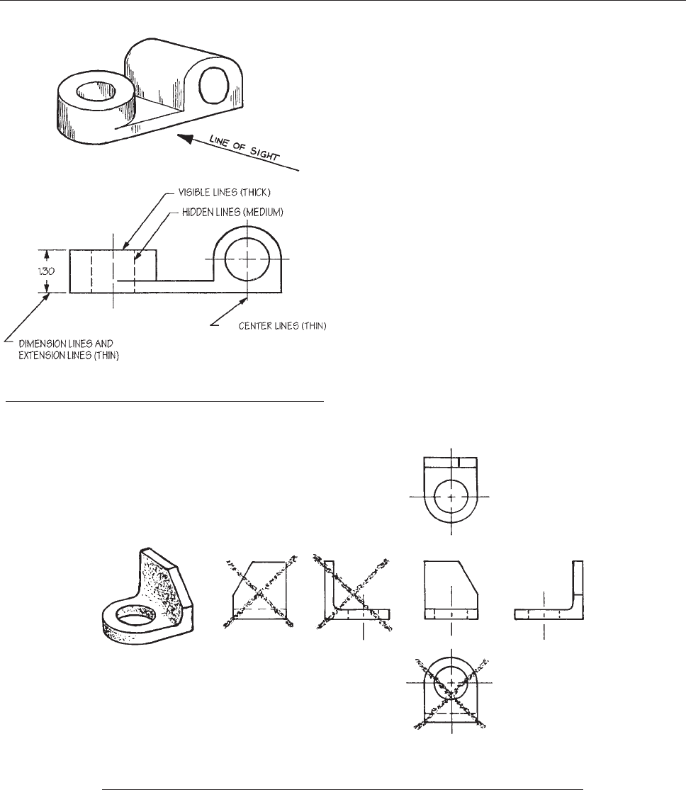
for thin lines. If only two line weights are available, medium
lines are shown thin. For pencil-and-paper work, H-grade
lead is used for heavy lines and lettering, 2H for medium
and light lines, 4H for layout.
The shape of an object is described by orthographic
projection. This is the view that one obtains when an object
is far from the eye so that there is no apparent perspective.
There are six principal views of an object, as illustrated in
Figure 1.29. As indicated in the illustration, not all views
are
required to completely describe an object. The drafts-
man should present only those views that are necessary for
a complete description.
In America the relative position of the views i n ortho-
graphic projection must be as shown in Figure 1.29.Thus
th
e view seen from the right side of an object is placed
to the right of the front view; the view seen fr om the top
is placed above the front view. This is the so-called
third-angle projection. Of course, for clarity or conven-
ience, the draftsman is i nitially free to choose any side
of the o bjec t a s t he ‘‘front.’’ In Europe and Asia the first-
angle projection is empl oyed (Figure 1.30). In this
projection
the view shown to the left of the front view
Figure 1.28 Lines used in mechanical drawing exemplified
in a CAD drawing of a side view of the object at the top.
Figure 1.29 The six principal views of the bracket shown on the left. This is a third-angle
projection. This is the preferred projection in the New World. The views not required to
describe the bracket in this particular case have been crossed out.
MECHANICAL DRAWING 41
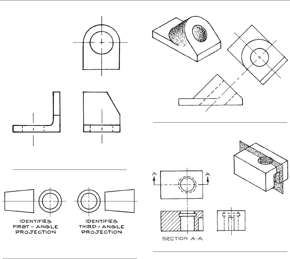
represents what would be seen i f the object in front view
wer e r olled to the left; the view shown above the front
view represents what would be seen were the object in
front view rolled 90° upwards. Of course it is very impor-
tant that anyone who views a drawing understands the
convention being used. Fi gure 1.31 shows orthographic
projecti
ons of a ‘‘tapered stopper’’ that can be unambig-
uously identified as either a first-angle projection (on
the left) or a third-angle projection (on the right). These
‘‘pictograms’’ are recommended f or use a s symbols on
drawings to confirm the projection intended by the drafts-
man. In this text, the third-angle projection is employed
throughout.
In some cases an auxiliary view will simplify a presen-
tation. For example, a view no rma l to an inclined surface
may be easie r to draw a nd more informative than one
of the six principal views. Such a case is illustrated in
Figure 1.32 . The relationship of the auxiliary view to the
Figure 1.30 A first-angle projection of the bracket
shown in Figure 1.29. This is the projection preferred
in
Europe and Asia.
Figure 1.31 One or the other of these pictograms can be
placed on a drawing to distinguish a ‘‘third-angle
projection’’ from a ‘‘first-angle projection.’’
Figure 1.32 Effective use of an auxiliary view.
Figure 1.33 Full section along the indicated plane.
42 MECHANICAL DESIGN AND FABRICATION
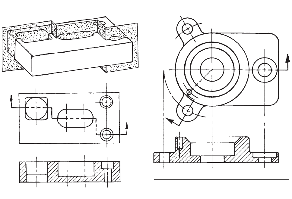
front v iew must be as shown. That is, the auxiliary view
of an inclined surface must be placed in the direction of
the normal to the s urfa ce. No te t he extens ion of th e cen ter
line from the auxiliary view to the front view to show the
direction of the auxiliary view.
Often the internal structure of an object cannot be
clearly indicated with hiddenedgesindicatedbydashed
lines. In this case it is u seful to show t he view that would
be seen if the object were cut open. Such a view is called
a section. An example of a full section is shown in
Figure 1.33.Thecutting
plane in the section is repre-
sented by cross-hatching with fine lines to suggest a
saw cut. The cross-hatch lines should always be at an
oblique angle to the heavy lines that indicate the outline
of the section. If the cutting plane extends through more
than one part of an assembly, the cross-hatch lines on two
adjacent parts should be in dist inctly different directions.
The cutting plane in a view perpendicular to the section
is shown by a heavy section line of alternating long
and two short dashes. Arrows on the section line indi cate
the direction of sight from which the section is viewed.
Sections may be identified with letters at each end of the
cutting-plane line.
It is often useful to have the cutting plane change direc-
tions so that it passes through several features. Angled
surfaces are then revolved into a common plane and offset
surfaces are projected onto a common plane to give an
aligned section, as illustrated in Figures 1.34 and 1.35,
ra
ther than a true projection of the cutt ing plane.
Other convenient sectioning techniques include the half
section of a symmetrical object, as shown in Figure 1.36,
and
the revolved section of a long bar or spoke, as shown in
Figure 1.37.
Man
y details, such as screw threads, rivets, springs, and
welds, are so tedious to draw, and appear so often, that they
are designated by symbols rather than faithful representa-
tions. Symbols for threads are illustrated in Figure 1.38.
Figure 1.34 An aligned view.
Figure 1.35 An aligned section.
MECHANICAL DRAWING 43
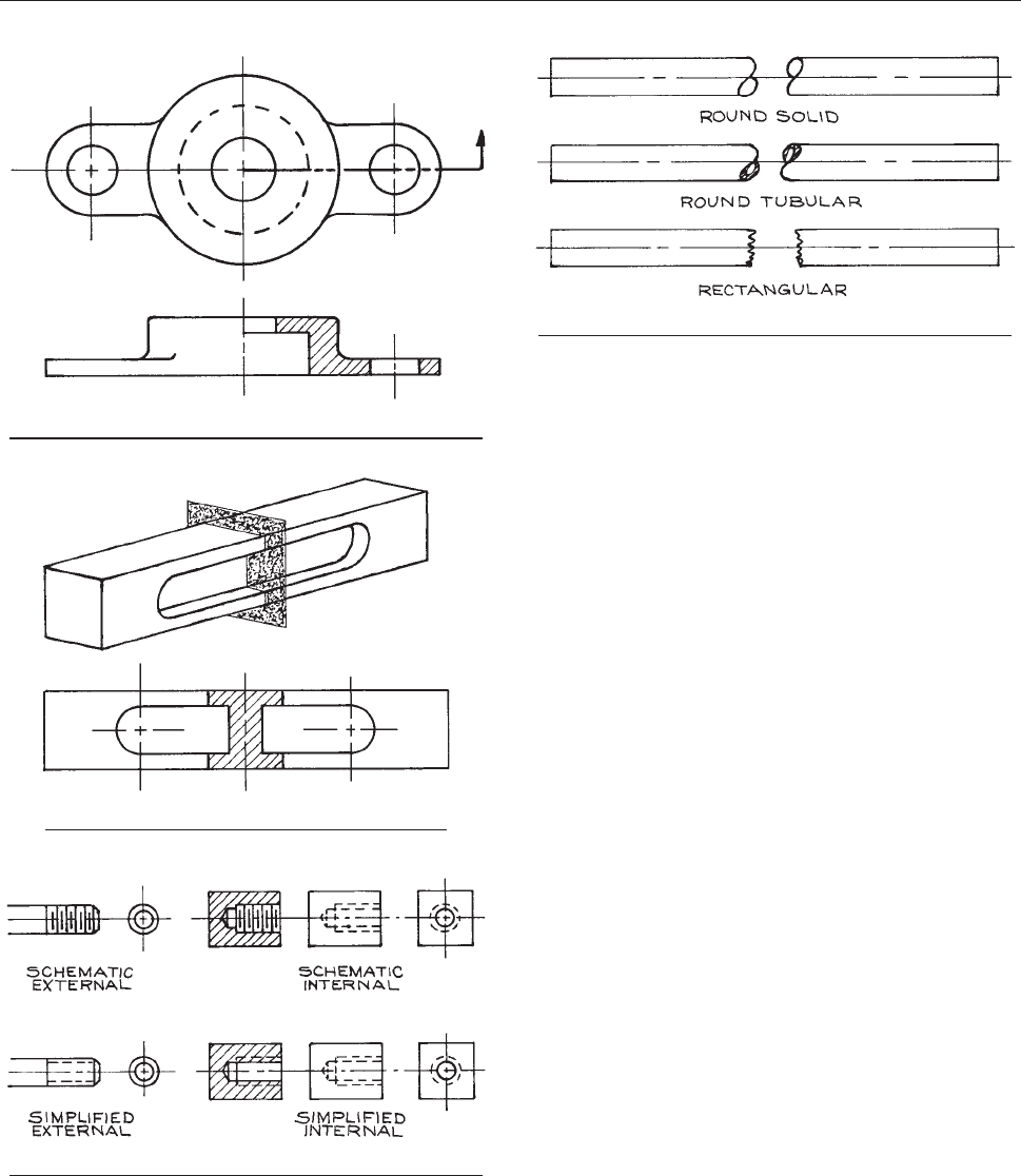
Drawings of parts too long to be conveniently fitted on a
piece of drawing paper can be represented as though a
piece from the middle of the part had been broken out
and the two ends moved together. Three conventional
breaks are illustrated in Figure 1.39.
Mechanical
drawings include dimensions, tolerances,
and special descriptions and instructions in written form.
Lettering on mechanical drawings employs only uppercase
letters in a sans serif font. Letters about 6 mm (1/4 in.) high
are usually appropriate.
1.5.3 Dimensions
After the shape of an object is described by an ortho-
graphic projection, dimensions and notes on the drawing
specify its size. The dimensions to be specified depend
upon the function of the object and upon the machine
operations to be performed by the workman when fabricat-
ing the object.
Eitheradimensionoranotespecifiesdistanceona
drawing. A dimension indicates the distance between
points, edges, or surfaces (Figure 1.40). A no
te is a writ-
ten instruction that gives information on the size and
shape of a part (Figure 1.41). If SI units are intended,
the
linear unit of distance is the millimeter. In the New
World t he customary unit i n engineeri ng drawing is the
decimal inch. The c hoice of unit is stated in a note:
UNLESS OTHERWISE SPECIFIED, ALL DIMENSIONS
ARE IN MILLIMETERS (or IN INCHES , as applicable).
Apart from this note, the units of a dimension are not
ordinarily specified on a drawing. Contrary to usual
Figure 1.36 A half section.
Figure 1.37 A revolved section.
Figure 1.38 Thread symbols.
Figure 1.39 Breaks.
44 MECHANICAL DESIGN AND FABRICATION
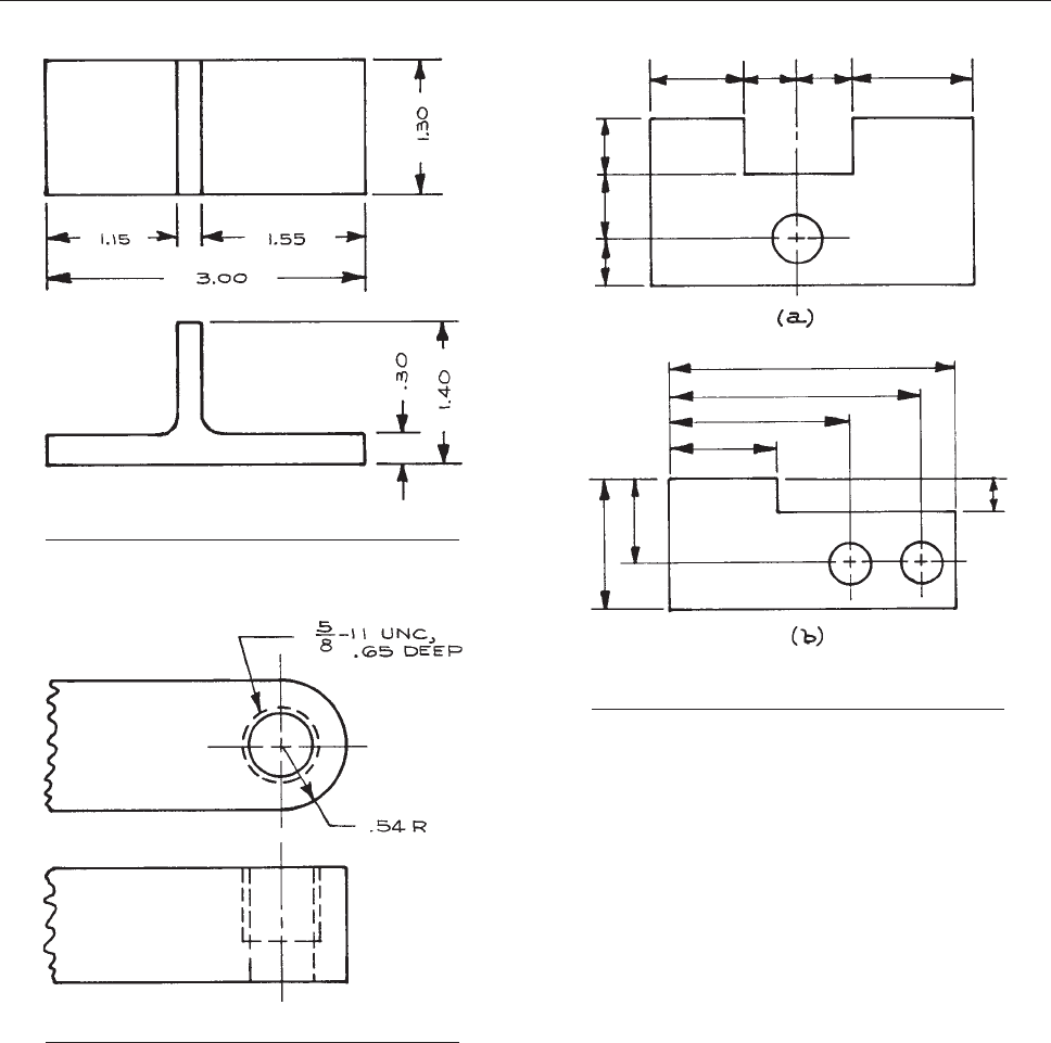
scientific practice, when dimensions are in inches, a dec-
imal dimension less than unity is written without a zero
preceding the decimal point: .256 rather than 0.256.Onthe
other hand, when specifying millimeter dimensions, a zero
precedes the decimal for a dimension less than one milli-
meter: 0.8 rather than .8.
Dimensions may be given in series or parallel
(Figure 1.42). If a combination of these two methods is
used,
care must be taken to ensure that the size of the
object is not over-determined. An example of an over-
dimensioned drawing is given in Figure 1.43. Dimensions
should
not be duplicated, and a drawing should include no
more dimensions than are required. When several features
of a drawing are obviously identical, it is only necessary to
dimension one of them.
Dimensions are often specified with respect to a datum.
This is a single feature whose location is assumed to be
exact. When choosing a datum, consider the functional
importance of locating other features of an object relative
to the datum, as well as the ease with which the workman
can locate the datum itself. (In Figure 1.46, the center of
the
.427R circular section serves as a datum point.)
Figure 1.40 Dimensions.
Figure 1.42 Dimensions: (a) series dimensions;
(b) parallel dimensions.
Figure 1.41 A note.
MECHANICAL DRAWING 45
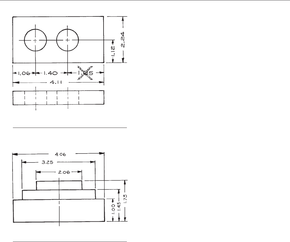
If possible, all dimensions should be placed outside
the view with extension lines leading out from the view.
As shown in Figure 1.42, the shorter dimensions are nearer
to
the object line. Dimension lines never cross extension
lines. Extension lines may cross extension lines if
necessary. Dimensions within the view are permissible to
eliminate long extension lines and if the dimension does
not obscure some detail of the view. The dimension closest
to the outside of a view should be about 12 mm (1/2 in.)
from the edge. Successive dimensions should be placed
at 9 to 12 mm (3/8 to 1/2 in.) intervals. Dimension values
should be staggered, as in Figure 1.44, rather than stacked
ver
tically or horizontally. Dimension values are oriented so
that they can be read from the bottom or the right side of
the drawing. Notice that the extension lines do not touch
the outline of the view, but rather stop about a millimeter
(1/16 in.) short.
Giving the diameter or radius, and dimensions to
locate the center of the radius of curvature, can specify a
round hole or circular part. As in Figure 1.43 and elsewhere,
th
e centerlines are extended to become extension lines.
Notes are used to specify the size of standard parts and
parts too small to be dimensioned. Notes are also used to
specify a feature that is derived from a standard operation
such as drilling, reaming, tapping, or spotfacing. Notes
such as ‘‘TAP 10-32 UNF, .75 DEEP’’ or ‘‘1/2 DRILL,
SPOTFACE .75D 3 .10 DEEP,’’ that refer to a specific
feature, are accompanied by a leader emanating from the
beginning or end of the note and terminating in an arrow-
head that indicates the location of the feature (Figure 1.41).
General
notes, such as ‘‘REMOVE BURRS’’ or ‘‘ALL
FILLETS 1/4 R,’’ that refer to the whole drawing, do not
require a leader.
Many abbreviations are used in writing dimensions and
notes. Common abbreviations used on mechanical draw-
ings are given in Table 1.4.
1.5.4 Tolerances
One of the most important parts of design work is the
selection of manufacturing tolerances so that a designed
part fulfills its function and yet can be fabricated with a
minimum of effort. The designer must car efull y and
thoughtfully specify the function of each part of an appa-
ratus in order to arrive at realistic tole rances on each
dimension of a drawing. It is important to appreciate
the c apabilities of the machines that will be used in
manufacture, and t he time and effort required to maintain
a given tolerance. As indicated in Figure 1. 45 ,thecost
of
production is approximately inversely related to the
tolerances.
Usually only one or two tolerance specifications will
apply to most of the dimensions on a drawing. It is then
convenient to encode the tolerance specification in the
dimension rather than affix a tolerance to each dimension.
In instrument design most dimensions are written as
Figure 1.43 An overdimensioned drawing. One
of the dimensions is superfluous.
Figure 1.44 Placement of dimensions and dimen-
sion values.
46 MECHANICAL DESIGN AND FABRICATION
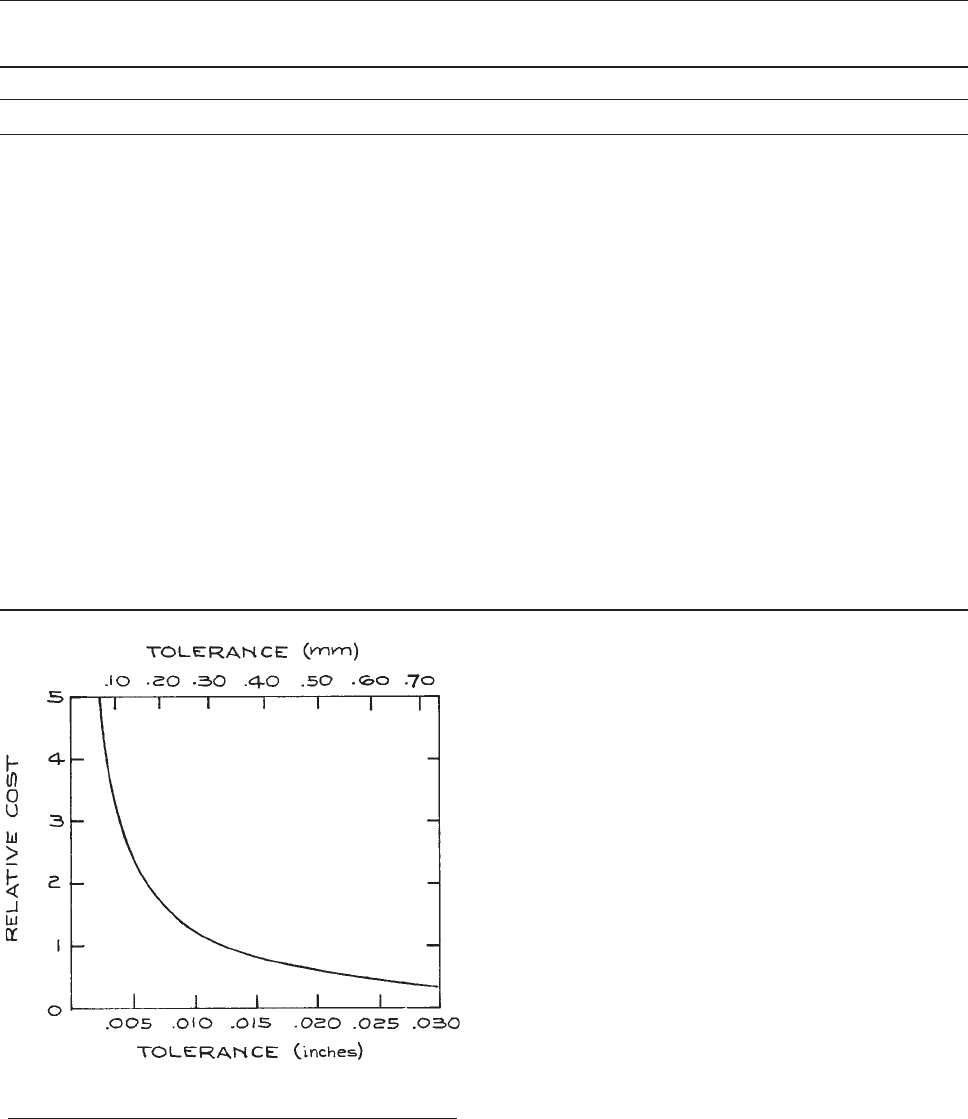
decimals. The number of decimal places of the dimension
can then indicate the tolerance on a dimension. Dimen-
sions expressed to two decimal places have one tolerance
specification, to three decimal places another, and so on.
The specifications are given in a note. An example of this
system is given in Figure 1.46.
Fractions
may be used in the American system to give
the size of some features derived from standardized oper-
ations, such as drilling or threading; similarly a whole
number millimeter specification may be used in the Euro-
pean system. A tolerance specification is unnecessary in
these cases, since both the designer and workman should
know what precision could be expected.
There are two methods of expressly stating the
tolerance on a dimension. The allowable variation, plus
and minus, may be stated after the dimension. Alterna-
tively, the limits of the dimension can be stated without
giving a tolerance at all. Examples of these two methods
are given in Figure 1.47. The trend is toward limit dimen-
sioning.
Table 1.4 Abbreviations Used on Mechanical Drawings
Word Abbr. Word Abbr. Word Abbr.
Bearing BRG Fillister FIL Right hand RH
Bolt circle BC Grind GRD Rivet(ed) RIV
Bracket BRKT Groove GRV Round RD
Broach(ed) BRO Ground GRD Root mean square RMS
Bushing BUSH Head HD Screw SCR
Cap screw CAP SCR Inside diameter ID Socket SOC
Center line CL Key K Space(d) SP
Chamfer CHAM Keyway KWY Spot face(d) SF
Circle CIR Left hand LH Square SQ
Circumference CIRC Long LG Stainless STN
Concentric CONC Maximum MAX Steel STL
Counterbore CBORE Minimum MIN Straight STR
Counterdrill CDRILL Not to scale NTS Surface SUR
Countersink CSK Number NO Taper(ed) TPR
Cross section XSECT Opposite OPP Thread(ed) THD
Diameter DIA, D, Ø Outside diameter OD Tolerance TOL
Drawing DWG Pipe thread PT T
ypical TYP
Drill(ed) DR Press PRS Vacuum VAC
Each EA Punch PCH Washer WASH
Equal(ly) EQ Radius R With W/
Fillet FIL Reference line REF Without W/O
Figure 1.45 Approximate relation between tolerance and
the cost of production.
MECHANICAL DRAWING 47
When the absolute size of two mati ng parts is not
important, but the clearance between them is critical,
specify the desired fit. Fits are classified as sli ding fits,
clearance locational fits, transition fits, interference fits,
and force fits. The uses of the various classes of fits and
tables of the tolerances required to give such fits are given
in standard texts on mechanical drawing.
Beware of an unde sirable accumulation of tolerances.
In series dimens ioning, th e tolerance on the distance
between two points separated by two or more dimensions
is equal to the sum of the tolerances for each of the
intervening dimensions. In Figure 1.42(a) the toler ance
on
the lateral location of the hole with respect to the right
side of the object is given by the sum of two tolerances.
For parallel dimensions, the location o f each feature
relative to the datum depends on only one tolerance;
however, the d ifference in t he distance between two loca-
tions depends upon two tolerances. In Figure 1.42(b),the
tolerance
on the distance between the two holes is given
by the sum of the tolerances on th e dimens ions that
locate the holes.
As much as possible, dimensions and tolerances should
be chosen so that materials can be used in their stock sizes
and shapes. Do not call for unnecessary finishing. For
example, the area around a hole in a casting or other rough
piece of metal can be spotfaced to provide a bearing sur-
face for a bolt if the quality of the rest of the surface is not
critical.
The dimensions and tolerances on a finished drawing
should be carefully checked. Imagine yourself as the
machinist who must use the drawing to make a part.
Proceed mentally through each step of the fabrication
to see that all necessary dimensions appear on the draw-
ing and that the specified dimensions are easy to use.
Also satisfy yourself t hat all desired tolerances are
within the capabilities of the anticipated machine-tool
operations.
1.5.5 From Design to Working Drawings
The first step in designing an instrument is to draw the
entire assembly. Start with rough sketches in pencil and
Figure 1.46 A decimal system for the specification of tolerances.
48 MECHANICAL DESIGN AND FABRICATION
paper before turning to the computer. Then, with the CAD
program, draw the outline of the most important parts
of the instrument. Work to full scale if possible. Add sub-
sidiary parts after the configuration of the essential ele-
ments has been established. Most dimensions, tolerances,
and fine details can be omitted at this point.
Pay attention to the manner in which pieces fit together.
Will the apparatus be convenient to assemble and disas-
semble? Is there sufficient clearance to insert bolts, pins,
and other fasteners? Are some parts much stronger or
weaker than required? Does a strong part depend upon a
weak one for location or support? Are all shapes as simple
as possible? Are standard shapes of materials and standard
bolts, couplings, bearings, and shafts used wherever pos-
sible?
Time spent at the drawing board mentally assembling
and disasse mbling a device will save hours of frustration
in the laboratory. Careful consideration of production
techniques c an save hundr eds of dollars in the shop.
With the initial orthographic drawing of the apparatus in
hand, it is wise to discuss it with the people who will do
the work.
After the design has reached its final form, the designer
must make a working drawing of each piece of the appa-
ratus. A working drawing is a fully dimensioned and tol-
eranced drawing to be used in the shop. Work to scale if
possible. The CAD program is especially useful at this
point. A new layer can be superimposed on the assembly
drawing and the outline of a single part transferred to the
new layer without fear of error. Alternatively the outline
of an individual part can be copied and transferred to a
new file. The draftsman should develop a systematic way
of naming drawings so they can be stored and easily
retrieved.
The critical test of a set of working drawings is their
usefulness. All necessary communication between scien-
tist and machinist should appear on the drawings. The
machinist should not require oral instructions, and should
not be required to make decisions affecting the perform-
ance of an instrument.
In the above discussion we have assumed that the sci-
entific designer has the services of a model shop. This is
the case in industrial laboratories and in many university
laboratories. The designer should follow the same proce-
dure when he fabricates his own apparatus. All questions
of sizes, tolerances, and fits must be answered before con-
struction. When a scientist attempts to make these deci-
sions as he proceeds with construction, the results are
invariably poor.
1.6 PHYSICAL PRINCIPLES OF
MECHANICAL DESIGN
No material is perfectly ri gid. W hen any member of a
machine is subjected to a force, no matter how small, it
will bend or twist to s ome extent. Even in the absence of
an external load, a mechanical element bends under its
own weight (so-called ‘‘body forces’’). A machine ele-
ment subj ect ed to a force that varies in time will vibrate.
A designer must appreciate the extent of deflection of
mechanical parts under load. The forces applied to or
contained by an a pparatus must be anticipated in specify-
ingthematerialanddimensionsofeachelement.The
Figure 1.47 Two methods of stating the tolerance
on a dimension: (a) as the allowable variation on a
dimension; (b) in terms of the allowable limits of
the dimension.
PHYSICAL PRINCIPLES 49
hallmark of a well-designed machine is that every el e-
ment bears the same level of stress and that stress does not
threaten the function of the machine or the capabilities of
the materials of whi ch the machine is constructed or the
fasteners that hold the parts together.
1.6.1 Bending of a Beam or Shaft
When a beam bends, one side of the beam experiences a
tensile load and the other a compressive load. Consider a
point in the flexed beam in Figure 1.48. The stress at this
point
depends upon its distance, c, from the centroid of the
beam in the direction of the applied force. The centroid is
the center of gravity of the cross section of the beam [see
Figure 1.48(b)]. The stress is given by:
s ¼
Mc
I
ð1:2Þ
where M is the bending moment at the point of interest
and I is the centroidal moment of inertia of the section of
the beam containing the point of interest. Cl early the
stress in a flexed beam i s greatest at the oute r surface of
the beam.
The centroidal moment of inertia of the section (more
correctly known as the second moment of the area of
the cross-section) is the integral of the square of the dis-
tance from the centroid multiplied by the differential
area at that distance. The integral is taken along a line
through the centroid and parallel to the applied force.
ForarectangularsectionofheightH and width B,such
as that shown in Figure 1.48 (b ), the centro idal moment of
inert
ia is:
I ¼
ð
B=2
B=2
ð
H=2
H=2
h
2
dhdb ¼
BH
3
12
ð1:3Þ
The centroidal moments of inertia of some common sym-
metrical sections are given in Figure 1.49.
The bending
moment is proportional to the curvature
produced by the applied force:
M ¼ EI
d
2
y
dx
2
ð1:4Þ
where y is the deflection produced by the force and E is the
modulus of elasticity of the material of which the beam is
composed. For the example given in Figure 1.48, assuming
the
weight of the shaft can be ignored, the bending moment
is simply:
M ¼FðL xÞð1:5Þ
where L is the length of the beam. The bending
moments for this and other simple systems are given in
Figure 1.50.
The
deflection of a stressed beam at a point a distance x
from a supported end of the beam depends upon the mod-
ulus of elasticity of the material, the centroidal moment of
the section of the beam, and the nature of the support. We
consider the case where the beam is rigidly fixed to its
support(s) (as in Figure 1.48) and the case where the beam
is
supported at each end by a simple fulcrum. Expressions
Figure 1.48 A flexed beam: (a) the beam bending under a load; (b) a cross section sowing
the centroid; (c) the distribution of shear forces along the long axis of the beam.
50 MECHANICAL DESIGN AND FABRICATION
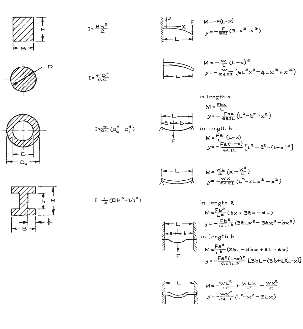
for the deflection of both point-loaded and uniformly
loaded beams are given in Figure 1.50.
A
sufficiently large bending moment will result in
the permanent deformation of a beam. This is the yield
point. A conservative relation between t he bending
moment at the yield point, M
y
, and the yield strength of
the material, s
y
, is given by M
y
¼ s
y
I/c
max
. [For the rec-
tangular sect ion beam supported at one end ( Fi gu re 1 . 48),
c
max
¼ H/2 and M
y
¼ s
y
BH
2
/6.] To determine the max-
imum allowable load on a beam or shaft one simply sets
M
y
equal to the expression fo r the maximum value of the
bending moment on the beam and solves f or the force.
Figure 1.49 Centroidal moments of inertia.
Figure 1.50 Bending formulae: M ¼ bending moment;
E ¼ modulus of elasticity; I ¼ centroidal moment of inertia;
w ¼ weight per unit length.
PHYSICAL PRINCIPLES 51

(For the re ctangular section beam supported at one end,
F
y
¼ s
y
BH
2
/6L.) In reality the yield strength of a beam in
bending is grea ter than for a beam i n tension, since the
inner fibers of the m aterial must be loaded to their yield
point to a cons iderable depth before the be am is perm a-
nently deforme d.
Even in the absence of applied forces, the e lements of
a machine bend under their own weight or if the machine
is otherwise accelerated or decelerated. An important
conclusion of the discussion above is that this effect is
reduced if the size of the machine is reduced; a mechan-
ical structure becomes stiffer as it is scaled down in size.
Consider a horizontal b eam of rectangular cross-section
cantilevered from a wall. From Figure 1.50, setting x ¼
L,
the weight of the beam causes a deflection at the
free end:
y
max
¼
wL
4
8EI
ð1:6Þ
where w is weight per unit length of the beam. Taking
w ¼ qBH,whereq is the weight density of the material of
the beam, and substituting for I gives:
y
max
¼
3qL
4
2EH
2
ð1:7Þ
If the dimensions of the beam are scaled down by a
factor f:
y
max
¼
3qð1LÞ
4
2Eð1HÞ
2
¼ f
2
3qL
4
2EH
2
ð1:8Þ
The deflection decreases as the square of the scale factor;
the relative deflection,
y
max
=
L
decreases linearly with the
scale factor.
It should be noted that all of the preceding discussion
assumes the tensile strength of a material to be the same as
the compressive strength. For materials such as cast iron
where this is not true, the bending equations are much
more complicated. The foregoing also ignores shear
stresses in a loaded beam. For very short beams, shear
stresses become important and the shear strength of the
material must be considered.
7
1.6.2 Twisting of a Shaft
The stress at a point in a hollow round shaft subjected to a
torsional load is:
s ¼
Tc
J
, J ¼
p
32
D
4
o
D
4
i
ð1:9Þ
where c is the distance of the point of interest from the
center of the shaft and T is the appl ied torque. J is
the centroidal polar moment o f inertia of the section of
the shaft, and D
o
,andD
i
are t he outer and inner diameters
of the shaft.
The total angle of twist in a shaft of length L is:
h ¼
57LT
GJ
deg ð1:10Þ
where G is the modulus of elasticity in shear, or shear
modulus, of the material of the shaft. For metals, the shear
modulus is about 1/3 the elastic modulus.
1.6.3 Internal Pressure
In the scientific lit erature, ‘‘high pressure’’ implies pres-
sures in excess of 1 GPa (15000 0 psi). Beyond 1 GPa
most fluids condense to s olid phases. At pressures in
excess of 1 GPa, remarkable pressur e-induc ed chemi cal
changes are observed. Not coincidently, 1 GPa corre-
sponds approximately to the yield strength of the stron-
gest materials. We shall not discuss here the special
technologies, notably the diamond anvil, that are requir ed
above 1 GPa.
To an engineer, 0.1 to 1 GPa is ‘‘ultrahigh pressure.’’ In
spite of what this term might i mply, familiar technologies
are appropriate. Ultrahigh pre ssur e t ub ing and tube fit-
tings, demountable joints, valves, and piston pumps are
commercially available (forexample,HighPressure
Equipment Company, PO Box 8248, Erie, PA 16505,
USA). As noted previously, scientific app ar atus to be
operated i n this pressure range should be built up entirely
of commercial components with coned and threaded
joints; joints brazed or welded in the lab or the local shop
are n ot safe or reliable at pressures above 0.1 GPa.
Indeed, consideratio ns of b oth safety and economics
52 MECHANICAL DESIGN AND FABRICATION

favor the use of commerc ial c omp onents when building
apparatus to operate at elevated pressures.
A pressure vessel should incorporate only cylindrical
sections if at all possible. The design and analysis of a
cylinder under internal press is easiest and most reliable.
Joints between cylindrical sections are most easily manu-
factured and assembled (see Section 1.4.10). Of course the
stress
exerted by an internal pressure is easily calculated
for vessels with other simple geometric shapes (spheres,
cones); their manufacture, however, can be daunting. In
any event, it is recommended that one design for at least
five times the anticipated pressure, unless a professional
engineer is consulted.
8
The maximum stress on a cylinder under internal pres-
sure is a tensile stress tangent to the inner surface of the
cylinder. For a cylinder with i nner and outer radii, R
1
and
R
2
, respectively, under pressure P, the maximum value of
this tangential stress, the so-called ‘‘hoop stress,’’ is:
s
t
¼
PðR
2
1
þ R
2
2
Þ
R
2
2
R
2
1
ð1:11Þ
Shearing forces are most often responsible for rupture in
ductile materials. The maximum shear stress is at the inner
surface where:
s
sheer
¼
PR
2
2
R
2
2
R
2
1
ð1:12Þ
For a thin-wall cylinder the expression for the hoop
stress reduces to:
s
t
¼ P
R
t
ð1:13Þ
where R is the inner radius and t the wall thickness, and it is
assumed t < 0.1R. The longitudinal (axial) stress and the
shear stress in this approximation are then just half the
hoop stress.
Expansion of a vessel under internal pressure may be an
issue in some instances. In the thin-wall approximation the
hoop strain is:
e ¼
PR
2Et
ð2 lÞð1:14Þ
where E is the modulus of elasticity and l is Poisson’s ratio
for the material of which the cylinder is made. Recalling
that strain is the increase in length per unit length, the
dilation, or radial growth of a cylinder under internal
pressure is:
d ¼
PR
2
2Et
ð2 lÞð1:15Þ
The longitudinal strain is:
e ¼
PR
2Et
ð1 2lÞð1:16Þ
The end closure of a cylindrical vessel may be spherical,
torospherical (elliptical in cross-section) or flat. The first
two are certainly more robust than a flat plate closure, but
the manufacture will be difficult and expensive. The stress
in a flat end plate depends upon how securely the end plate
is attached to the cylindrical vessel. If there is the possi-
bility of movement between the end plate and the cylinder
to which it is attached, such as for a removable, gasketed-
and-bolted, endplate, the maximum stress occurs at the
center of the plate where, for a plate of thickness d and
radius R:
s ¼
3
8
R
d
2
ð1 þ lÞP ð1:17Þ
The deflection under pressure at the center of the plate is:
d ¼
3PR
4
ð5 þ lÞð1 lÞ
16Ed
3
ð1:18Þ
For a permanently affixed flat closure, such as an end
plate welded to a cylindrical vessel, the maximum stress is
at the edge where the radial stress is:
s
r
¼
3
4
R
d
2
P ð1:19Þ
and the tangential stress is:
s
t
¼
3
8
R
d
2
ð1 þ lÞP ð1:20Þ
PHYSICAL PRINCIPLES 53
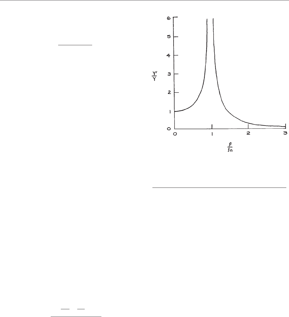
Deflection under pressure at the center of a permanently
fixed end plate is:
d ¼
3PR
4
ð1 l
2
Þ
16Ed
3
ð1:21Þ
Design for external pressure is discussed in Section
3.6.2 in the context of vacuum chambers.
1.6.4 Vibration of Beams and Shafts
In many instruments, vibration of a supporting beam or
shaft c an adversely affect operati on. The designer must
pay spe cial attention t o the natur al frequencies of vibra-
tion of the parts of an instrument. A periodic d isturbance
with a frequency near that of one of the natural fre-
quencies will induce a large and possibly destructive
vibration. For the purpose of illustration, the response
of an oscillator to the frequency of a driving force is
shown in Figure 1.51.
T
here a re two wa ys for the designer t o prevent destruc-
tive vibratio ns. The critica l element can be designed so
that its natural frequency of vibration is far removed from
the frequency of a disturbing force, or the disturbing force
can be in hi bited in the vicinity o f th e natural frequency o f
the critical element. The latter scheme is called damping.
Very low-frequency vibrations can be damped by a
hydraulic or friction shock absorber such as is employed
on automobile suspensions. High frequencies can be
damped by coup ling the objectionable source of vibration
to its surroun ding s th rough a member that has a very low
natural frequency of vibration. Mounts made of rubber or
cork are very effecti v e for absorbing high-frequency vibra-
tions and sudden shocks, since these materials possess a low
modulus of elasticity.
The fundamental frequency of vibration (in Hz) of a
shaft or beam with one or more concentrated masses
attached is given by:
f
2
n
¼
a
4p
2
ð
L
0
M
2
EI
dx
ð
L
0
qAY
2
dx þ +
i
F
i
Y
2
i
ð1:22Þ
where:
I ¼ centroidal moment of inertia of the shaft,
M ¼ M(x) ¼ maximum bending moment at x, i.e., the
amplitude of the bending moment induced by the forces on
the shaft at x,
a ¼ inertial acceleration experienced by the shaft and its
weights (for a nonrotating shaft, a ¼ g),
E ¼ modulus of elasticity of shaft material,
q ¼ weight density of the shaft [(q /g) is the mass
density],
A ¼ cross-sectional area of the shaft,
L ¼ length of the shaft
Y ¼y(x) ¼ maximum deflection of the shaft at x, i.e., the
amplitude of vibration at x,
F
i
¼ force exerted by the ith mass (for a nonrotating
shaft, this is the weight of the ith mass),
Y
i
¼ maximum deflection at the location of the ith
mass.
Figure 1.51 Response of a machine element to a
periodically varying force. Y# is the amplitude of
vibration of the element and f
n
is its natural frequency
of vibration. Y and f are the amplitude and frequency of
the driver.
54 MECHANICAL DESIGN AND FABRICATION

For a system similar to one of the static deflection
cases treated in Figure 1.50, one need only substitute the
appropriate
expressions for the bending moment and
deflections and solve the resulting equation to determine
the natural frequency. Consider for example a beam of
negligible mass that is rigidly supported at one end and
supports a mass of weight W at its free end. This is the case
illustrated at the top of Figure 1.50. The natural frequency
of
vibration is:
f
2
n
¼
g
4p
2
ð
L
0
W
2
L xðÞ
2
EI
dx
W
W
6EI
3Lx
2
x
3
x¼L
2
,
f
n
¼
1
2p
3gEI
WL
3
1=2
Hz: ð1:23Þ
In general, the shape of the deflection curve is not known.
However, the assumption of some reasonable deflection
curve usually will provide a useful result. In most cases
one can assume a sine curve for a shaft supported (but
not clamped) at both ends, or a parabola for a shaft sup-
ported at only one end. More precise approaches to com-
plex systems are given in many engineering texts on
vibration.
9
Consider once again the beam of negligible mass, rig-
idly supported at one end, with a weight W at the free end.
A parabolic deflection curve with the correct limit proper-
ties is given by:
y ¼
y
0
L
2
L xðÞ
2
ð1:24Þ
where y
o
is the maximum deflection of the free end. The
bending moment is then:
M ¼ EI
d
2
y
dx
2
¼EI
y
0
L
2
: ð1:25Þ
Substituting in the equation for the natural frequency
gives:
f
2
n
¼
g
4p
2
ð
L
0
2EI y
0
=L
2
EI
dx
W y
0
ðÞ
2
f
n
¼
1
p
gEI
WL
3
Hz ð1:26Þ
in reasonable agreement with the exact solution derived
above.
For the special case of a heavy shaft or beam with a
centrally placed load, a correct solution can be derived
by assuming the shaft to be weightless and adding half
the weight of the shaft to the concentrated load.
1.6.5 Shaft Whirl and Vibration
A shaft and rotor can never be perfectly balanced, and the
axis of rotation can never be exactly located by the shaft
bearings. As a shaft rotates, centrifugal force on the unbal-
anced mass deflects the shaft and causes it to whirl around
its axis of rotation. This whirling motion appears as a vibra-
tion to a stationary observer, and can be treated as such.
There is a critical speed at which the whirl becomes violent.
In this unstable condition, the shaft or its bearings are likely
to be damaged and intense vibration will be transmitted
through the bearing mount to other parts of the machine.
This critical condition occurs when the shaft speed (in rps)
equals the natural frequency (in Hz) of the stationary shaft
and rotor assembly. It follows that the mathematical deriva-
tions of natural frequencies of assemblies of beams and
weights can be applied to the calculation of critical speeds
for shafts and rotors. The actual centrifugal loads on the
rotating shaft need not be determined. This is because the
load F always appears as the ratio F/a and:
F
a
¼
W
g
¼ m ð1:27Þ
where W is the weight of the element that is ex erting the load.
The critical speed for a rotor-shaft assembly depends
upon how rigidly the shaft bearings support the shaft.
Two extreme cases are considered: a thin bearing, such
PHYSICAL PRINCIPLES 55

as a ball bearing, for which the angle of the shaft passing
through the bearing is not fixed; and a thick bearing, such
as a plain sleeve bearing, that rigidly maintains the angular
alignment of the shaft. The critical speed for a rotor on a
weightless shaft supported on thin bearings is:
n
c
¼ 0:276
gEIL
Wa
2
b
2
1=2
rps ð1:28Þ
where W is the weight of the rotor, I is the centroidal
moment of inertia of the shaft, E the modulus of elasticity
of the shaft material, L the length of the shaft between the
bearings, and a and b are the distances from the rotor to the
bearings. If the ends of the shaft are rigidly supported in
long bearings the critical speed is:
n
c
¼ 0:276
gEIL
3
Wa
3
b
3
1=2
rps ð1:29Þ
Notice that the critical speed can be increased by placing
the rotor near one end of the shaft so that a or b is small.
In this case the rotor acts as a gyro tending to stiffen the shaft.
For an unloaded shaft on thin bearings the critical
speed is:
n
c
¼ 1:57
EIg
qAL
4
1=2
rps ð1:30Þ
and for an unloaded shaft on long bearings:
n
c
¼ 3:53
EIg
qAL
4
1=2
rps ð1:31Þ
where q is the weight density of the shaft material. The
units of the individual quantities appearing in brackets in
the four equations above must be such that overall the
quantity in brackets has units of s
2
. For the particular case
of a solid, round, steel shaft the critical speeds are:
The special case of a centrally placed rotor on a heavy
shaft can be treated by adding half the weight of the shaft
to the rotor and taking the shaft to be weightless. The
critical speed for a shaft carrying several rotors can be
approximated by:
n
c
¼
1
n
2
s
þ +
i
1
n
2
i
1=2
ð1:33Þ
where n
s
is the critical speed of the shaft alone and n
i
is
the critical speed for the ith rot or alone on a weightless shaft.
The designer must manipulate the dimensions and mate-
rial of a shaft and rotor, and the location of the rotor, so that
its critical speed does not coincide with the design speed of
an assembly. It is usually sufficient for these two speeds to
differ by a factor of
ffiffiffi
2
p
. The most desirable situation is for
the critical speed to exceed the design speed. If this is not
possible, the drive motor for the rotating assembly should be
so powerful that the shaft accelerates very rapidly through
the region of the critical speed. The drive motor will require
an excess of power because considerable power is dissipated
to vibration at the critical speed.
The formulae above give the lowest frequency of vibra-
tion and the lowest critical speed for a shaft and rotor
assembly. A shaft with a number of weights has as many
different fundamental modes of vibration as it has weights.
In addition, vibration will occur at harmonics of the fun-
damentals.
For rotational speeds far away from a critical speed, a
rotating assembly can be considered to be rigid. Neverthe-
less, imbalance can lead to inertial (centrifugal) forces that
may damage the shaft or its bearings. If the unbalanced
mass lies within a plane perpendicular to the axis of
n
c
¼ 80 000
D
L
2
rps ½thin bearings; D ¼ diameter ð in:Þ; L ¼ length ðin:Þ
¼ 3 150
D
L
2
rps ½thin bearings; D ¼ diameter ðmmÞ; L ¼ length ðmmÞ
n
c
¼ 180 000
D
L
2
rps ½long bearings; D ¼ diameter ðin: Þ; L ¼ length ðin:Þ
¼ 7 100
D
L
2
rps ½long bearings; D ¼ diameter ðmmÞ; L ¼ length ðmmÞ ð1:32Þ
56 MECHANICAL DESIGN AND FABRICATION

rotation, as for the case of a thin rotor on a shaft, the rotor
can be statically balanced. The condition for static balance
is that the axis of rotation passes through the center of
gravity. In practice this can be accomplished by placing
the shaft with its rotor across a pair of knife-edge rails.
The shaft will roll or rock until coming to rest with the
unbalanced inertial force pointed radially downwards.
Weight is then added or removed along the vertical radius
until balance is achieved.
If there are unbalanced masses acting at different points
along the axis, then dynamic balancing is required. The
conditions for dynamic balance are that the axis of rotation
passes through the center of gravity and that the axis of
rotation coincides with a principal axis of the inertial force.
Dynamic balancing is difficult without specialized equip-
ment. Balancing is done inexpensively and accurately as a
commercial service.
1.7 CONSTRAINED MOTION
In addition to a rigid support structure, most machines
include some moving parts. The motion of these parts must
usually be constrained in some fashion to obtain the
required function. Most often the desired motion is trans-
lation in a plane or along a line, or rotation about one or
more axes. The design of the constraining mechanism for a
moving part must meet dimensional, strength, and wear-
resistance specifications.
To achieve constrained motion the designer may either
create a support structure for the moving part that will give
the desired alignment, or make use of a standard, commer-
cially available machine element. In the former case, it is
necessary to understand the principles and limitations of
geometric design. In the latter, the designer must be famil-
iar with the range and precision of commercial bearings,
shafts, sliders, and so on. The economics of the choice
should not be ignored.
1.7.1 Kinematic Design
A rigid body has six independent degrees of freedom of
motion. These are usually taken to be the translational
motions along three or tho gona l axes through the center
of gravity and the rotational motions about these axes.
Any motion can be described as a linear combination of
these six motions. Similarly, six coordinates define the
position of a body: three p ositi on coordina tes and th ree
angle coordinates. Motion is constrained and the number
of degrees of freedom is reduced if one o f these coordi-
nates is fixed or if some linear combination of these
coordinates is fixed. For example, a rigid object will be
constrained to move in a plane if one of its position coor-
dinates is fixed. Kinematic design for constrained motion
consists of fixing a point on a body for each degree of
freedom to be constrained.
10
In general, one degree of freedom can be removed by
constraining a point on a body to remain in contact with a
reference surface. The following examples illustrate this
principle of kinematic design:
(1) Consider a sphere constrained to maintain point con-
tact with each of two reference planes: a ball resting in
a V-groove. The ball is free to rotate about any axis,
but it can only translate along a line parallel to the
intersection of the planes. The ball has lost two
degrees of freedom.
(2) A three-legged ‘‘milking stool’’ that is constrained to
maintain three points of contact with a plane surface
has only three degrees of freedom: translation in two
directions parallel to the plane and rotation about an
axis perpendicular to the plane.
(3) A body in contact at three points with a cylindrical
surface has three degrees of freedom: translation in
the direction of the cylinder axis, revolution about the
cylinder axis, and rotation about an axis perpendicular
to the plane defined by the three points of contact.
The object of kinematic design is to permit motion to be
constraine d wit hout d ep end ing up on pr ec ision of ma nu -
facture. A co mpl icatio n exists if two contact point s are
degenerate in the sense that the function of the two points
can be served b y a si ngle point of co nt ac t. Conside r a
four-legged table vis-a
`
-vis a three-legged table. One of
the four legs provides a degenera te point of contact with
the floor. The fourth leg may provide some much-needed
stability, but it also introduces uncertainty in the location
of the table t op unless all four legs are of precisely the
same length. Of course, the sort of c onsid erat ion s that
lead to the production of four-legged tables often dictates
CONSTRAINED MOTION 57
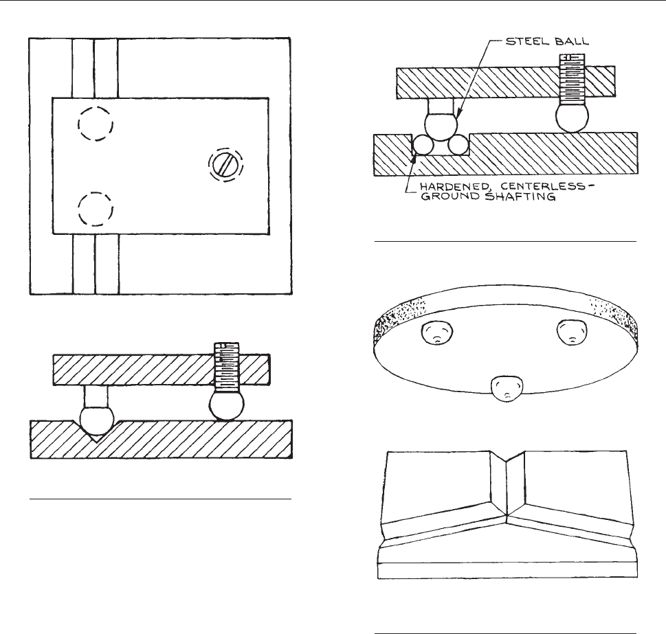
a semikinematic or degenerate kinematic design for other
devic es as well.
Kinematic designs are illustrated in Figures 1.52–1.54.
Th
e ball feet on the carriage shown in Figure 1.52
provide five points of c ontact b etween the carriage and
its
base. Thus the carriage is only free to slide in one
direction. One problem with this design is that it is diffi-
cult to mill a V-groove with smooth surfac es. The s urface
quality o f t he g roove can be improved by lapping with
carborundum, u sing a V-shaped brass lap that fits in the
gro ove.
An improved version of the design in Figure 1.52 is
sho
wn in Figure 1.53. A pair of steel rods replaces the
V
-groove, and balls replace the feet of the carriage. This
design is both more precise and more economical than the
previous one. Stainless-steel shafting, hardened and cen-
terless-ground to a diameter tolerance of 60.001 mm
(6.00005 in.), is available at a cost of a few euros a foot.
Stainless-steel balls with a roundness tolerance of 60.001
mm are also inexpensive. The channel that contains the
rods must be milled, but the surface quality in this channel
is not critical. In a milling operation, the sides of the
Figure 1.52 Kinematic design that constrains a
carriage to move in a straight line.
Figure 1.53 An improved version of the design
shown in Figure 1.52.
Figure 1.54 Kinematic design that permits an
accurately located part to be removed and replaced
in the same position.
58 MECHANICAL DESIGN AND FABRICATION
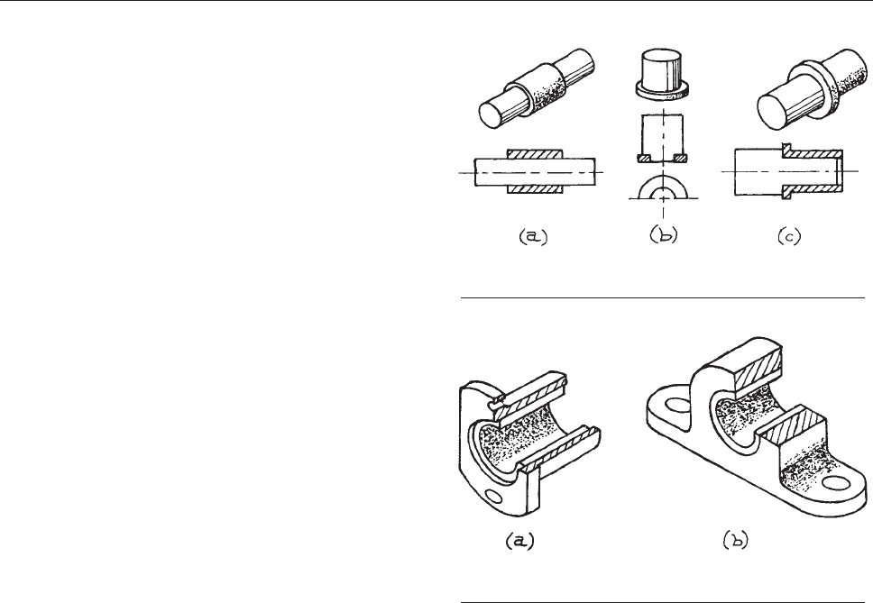
channel can easily be kept straight and parallel to within
0.01 mm/m (.0001 in./ft.).
The three grooves in the platform shown in Figure 1.54
allow precise relocation of a three-legged table after it has
been
removed. The ball feet of the table make six points of
contact with the platform, so that there are no degrees of
freedom.
In applying the principles of kinematic design it must be
borne in mind that all materials are more or less elastic.
Deformation or deflection of the elements of a kinematic
structure under load leads to a deviation from true kinematic
behavior. In the absence of careful analysis of such effects, it
is often possible to obtain higher precision location or move-
ment, as well as greater stability, through the use of standard,
nonkinematic elements such as bearings and ball sliders.
Smith and Chetwynd discuss the analysis and exploitation
of elastic deformation on kinematic designs in their excel-
lent book on the design of precision mechanism.
11
1.7.2 Plain Bearings
A bearing is a stationary element that locates and carries
the load of a moving part. Bearings can be divided into two
categories depending upon whether there is sliding or
rolling contact between the moving and stationary parts.
Sliding-contact bearings are called plain bearings. Rolling
bearings will be discussed in the next section.
Plain bearings may be designed to carry a radial load,
an axial load, or both. Different types are illustrated in
Figure 1.55. A radial bearing consists of a cylindrical shaft
or journal rotating
or sliding within a shell, which is the
bearing proper. The entire assembly is referred to as a
journal bearing. An axial bearing consists of a flat bearing
surface, like a washer, against which the end of the shaft
rests. These are called thrust bearings. A journal bearing
may incorporate a flanged journal, in which case it will
support a radial load as well as an axial load.
A journal is usually hardened steel or stainless steel.
Precision-ground shafts and shafts with precision-ground
journals are available in diameters from 1 to 25 mm (1/32
to 1 in.). Bearing shells of bronze or oil-impregnated
bronze are available to fit. Nylon bearings for light loads
and oil-free applications are also available. Commercial
shafting and bearings are manufactured to provide a clear-
ance of 0.005–0.02 mm (.0002–.0010 in.).
Many different methods of lubrication can be employed
instead of oil impregnation. The inner surface of the bear-
ing can be grooved, and oil or grease can be forced into the
groove through a hole in the shell. If oil is objectionable, a
groove on the inner surface of the bearing can be packed
with molybdenum disulfide or other dry lubricant.
A plain bearing is installed by pressing it into a hole in
the supporting structure. An interference of about 0.03 mm
(.001 in.) is desirable for bearings up to an inch in diam-
eter. That is, the outer diameter of the bearing shell should
be about 0.03 mm (.001 in.) larger than the hole into which
it is pressed. If the interference is too great, the inner
diameter of the bearing may be significantly reduced.
A variety of bearing housings and pillow blocks (Figure
1.56) are available. These mountings are bored to accept
standard
bearings and in many instances the bearing is
premounted. These mounts replace precision-bored bear-
ing mounts.
Figure 1.55 Plain bearings: (a) a journal bearing; (b) a
thrust bearing; (c) a flanged jour nal bearing.
Figure 1.56 (a) A bearing housing; (b) a bearing mounted
in a pillow block.
CONSTRAINED MOTION 59
It is usually necessary to provide axial location for a
shaft in a journal bearing. This can be accomplished with
a retaining ring in a groove on the shaft (Section 1.4.4) or a
collar secured by a setscrew.
Plain bearings run smoothly and quietly, and have a high
load-carrying ability. Properly installed and lubricated,
they have a very long life. Because of the close clearances
between parts, they are not easily fouled by dirt in their
environment. Plain bearings are limited to relatively low-
speed operation. Speeds in excess of a few hundred rpm
are not practical without forced lubrication. The primary
disadvantage of plain bearings is their high starting fric-
tion, although, when properly installed and lubricated,
their running friction can be very low.
1.7.3 Ball Bearings
The rolling element in a rolling contact bearing may be a
ball, cylinder, or cone. Ball bearings are used for light
loads and high speeds. Roller bearings employing cylin-
drical or conical rollers are suitable for very heavy loads,
but are not often used for instrument work. We shall dis-
cuss only ball bearings.
As with plain bearings, there are both radial and thrust
ball bearings (Figure 1.57). A radial
ball bearing consists
of an inner and an outer race with a row of balls between.
The grooves in each race have a radius slightly larger than
the radius of the balls so that there is only point contact
between the balls and the race. The balls are separated by a
retainer that prevents the balls from rubbing against one
another and keeps them uniformly spaced around the bear-
ing. A radial ball bearing can tolerate a substantial thrust
load, but for pure axial loads a thrust bearing should be
used. A thrust bearing is similar to an axial bearing except
that it has upper and lower races rather than inner and outer.
Ball bearings are made of steel or stainless steel. They are
graded 1, 3, 5, 7, or 9 dependingon manufacturing tolerances.
Grades7and9havegroundracesandaremadetotheclosest
tolerances. They cost little more than lower-grade ones and
should be specified for instrument applications.
Proper installation is required to obtain good perform-
ance from a ball bearing. The rotating race should be given
a firm interference fit, and the stationary race given a light
‘‘push fit’’ to permit some rotational creep. This slight
movement of the stationary race helps prevent the maxi-
mum load from always bearing on the same spot.
Press fitting changes the internal clearances in a bearing.
Bearing manufacturers specify the amount of interference
that should be used. As shown in Figure 1.58, the press
arbor
used to drive a bearing onto a shaft or into a housing
should be designed so that the thrust is not transmitted
through the balls. Never hammer a bearing into place.
Figure 1.57 Ball bearings: (a) a radial ball bearing;
(b) a thrust ball bearing.
Figure 1.58 Installation of a bearing. The press
arbor should bear on the race that is being fitted.
60 MECHANICAL DESIGN AND FABRICATION
The surface quality and diameter tolerance of the shaft
that is to be fitted into a bearing, or the hole that is to house
a bearing, must be of the same quality as the bearing. For
high-quality bearings the mounting surfaces should be
ground. Centerless-ground precision shafting is available
to fit all standard bearings. Bearing mounts and pillow
blocks with premounted bearings are similarly available
to eliminate the need for precision machine work when
installing ball bearings.
Ball bearings are designed with both radial and axial
clearances. This play is intended to allow for axial misalign-
ment and for dimensional changes that occur upon installa-
tion or because of thermal stresses. For the best locational
precision and to obtain smooth, vibration-free operation, a
ball bearing should be pr eloaded to remove most of this play.
A preloading force that displaces one race axially with
respect to the other will remove both radial and axial play
by causing the balls to roll up the sides of their groov es. The
use of a shim to take up the play in a bearing is illustrated in
Figure 1.59. For light-duty applications, the end play can
also
be taken up by installing a spring washer (Section
1.
7.5) instead of a shim. W ith proper installation, a ball
bearing
will locate a revolving axis to within a few thou-
sandths of a millimeter (ten-thousandths of an inch).
Bearings must be protected from effects that damage the
race surface on which the balls roll. Ball bearings are most
likely to fail because of occasional large static loads that
produce an indentation in the race. Such a dent is called a
brinell. Dynamic loads are distributed around the race and
are less likely to cause damage; however, a hard vibration
can cause brinelling in the form of a series of dents or
waves on the surface of a race. Of course, a bearing is also
damaged by the introduction of foreign matter that abrades
or corrodes the bearing surfaces.
Bearings should be lubricated with petroleum oils or
greases. For high speeds and light loads the lightest, finest
grades of machine oil can be used. Ball bearings require
very little oil. Lubrication is sufficient if there is enough oil
to produce an observable meniscus at the point where each
ball contacts a race.
Cleanliness is important. In a dirty environment, bear-
ings with built-in side shields should be used. It is probably
wise to use enclosed bearings in all instrument applications
to keep the bearings clean and to prevent oil from contam-
inating the environment.
The chief advantages of ball bearings are their low starting
friction and very low running friction. They are well suited to
high-speed, low-load operation. Relativ e to plain bearings,
ball bearings are noisy and occupy a large volume. The cost
of quality ball bearings is so small that economic consider-
ations are usually not important in choosing between rolling
bearings and plain bearings for an instrument.
1.7.4 Linear-Motion Bearings
A linear-motion bearing may be of either the sliding or
rolling type. A plain journal bearing can be used to locate
a shaft that is to move axially. A V-shaped or dovetail
groove sliding over a mating rail can serve as a bearing
between a heavily loaded, slowly moving carriage and a
stationary platform. This is the type of bearing used
between the carriage and the bed of a lathe.
Linear ball bearings are commercially available. In a
bearing for use with an axially moving shaft, the balls that
carry the load between the outer race and the shaft move in
grooves that run parallel to the axis of the shaft. The balls
are recirculated through a return track when they roll to the
end of a groove. Linear-motion ball bearings will locate a
shaft to within 60.005 mm (6.0002 in.) of a reference
axis. Their cost is comparable to conventional rotating ball
bearings. Complete roller-slide assemblies are also avail-
able. These employ balls rolling in V-grooves. Roller slides
will maintain straight-line motion to within 0.002 mm per
centimeter (.0002 in. per inch) of travel.
Figure 1.59 Installation of a shim to remove end play in a
shaft mounted on ball bearings.
CONSTRAINED MOTION 61

1.7.5 Springs
In many instances it is desirable for a motion to be con-
strained by a flexible element such as a spring. Springs are
used to hold two parts in contact when zero clearance is
required, to absorb shock loads, to damp vibrations, and to
measure forces.
A spring is characterized by the ratio of the magnitude
of applied force to the resulting deflection, d. This is the
spring rate:
k ¼
F
d
ð1:34Þ
As is the case for any flexible system, an assembly con-
sisting of a spring and attached load has a natural fre-
quency of vibration:
f
n
¼
1
2p
k
m
1=2
Hz ð1 :35Þ
where m includes the mass of both the spring and any load
that is affixed to it. Since m ¼ W/g ¼ F/a,wehave,upon
substituting for the spring rate in this equation
f
n
¼
1
2p
g
d
st
1=2
Hz, ð1:36Þ
where d
st
is the static deflection produced by the weight of
the spring plus the attached load.
In most applications it is desirable to choose a spring
that will not resonate with any other part of the apparatus
into which it is installed. If the spring is expected to damp a
vibratory motion, its natural frequency should differ from
that of the disturbance by more than an order of magnitude.
A spring will exert an uneven force wh en it is subjected
to a p eri odic ally varying load whose frequency is close to
the natural frequency of the spring. When the vibration
of the spring is in phase with the load, the reactive force
of the spring will be less than its static force for any given
deflection. When the spring is out of phase with the load,
it will exert a greater force than expected. This phenomenon
is called surge. Surge can be reduced or eliminated by using
two springs with different natural frequencies. In the case
of helical springs, they can be placed one inside the other.
In instrument work, helical springs are most often used.
Helical torsion, extension, and compression springs are
illustrated in Figure 1.60. The number of coils in a helical
spring
must be sufficient to ensure that the spring wire
remains within its elastic limit when the spring is at max-
imum deflection. The number of coils in a compression
spring also determines the minimum length that is realized
when successive coils come into contact. A long compres-
sion spring may buckle under stress. This tendency is dis-
couraged if the ends of the spring are square. It can be
prevented by placing a rod through the center or by instal-
ling the spring in a hole. In general, a compression spring
must be supported by some means if its length exceeds its
diameter by more than a factor of five.
The spring rate of a helical spring made of round wire is:
k ¼
Gt
4
8D
3
N
ð1:37Þ
where G is the shear modulus of the spring material (about
1/3 of the elastic modulus), t the diameter of the wire, N the
number of coils, and D the mean diameter (the average of
the inner and outer diameters) of the spring. The natural
frequencies for free vibrations are:
f
n
¼
nt
4pND
2
gG
q
1=2
Hz ð1:38Þ
where q is the weight density of the spring wire and n is an
integer. For steel wire:
f
n
¼
14000nt
ND
2
Hz ðD and t in inchesÞ
¼
550nt
ND
2
Hz ðD and t in millimetersÞð1:39Þ
A variety of steels and bronzes are used for spring
manufacture. High-carbon steel wire works well. If
Figure 1.60 Springs: (a) helical torsion spring; (b) helical
extension spring; (c) helical compression spring.
62 MECHANICAL DESIGN AND FABRICATION
necessary the spring can be wound in the annealed state
and hardened after forming. Music wire, or piano wire, is
one of the best materials for one-off construction of
small springs. It is available in diameters of 0.1 to 3
mm (.004 to .103 in.). This wire is very strong and hard
because of the drawing process used in its production,
and doe s not ne ed to be hardene d after fo rming.
Type-302 stainless-s teel wi re is u seful for springs that
are subject to a corrosive environment. Springs of ber-
ylli um–copper wire are especially useful in applications
where spring deflection is used to gauge a force, since this
material maintains a linear stress–strain relation almost
to the point of permanent deformation. As mentioned
earlier, quartz fiber torsion springs can also be used in these
applications.
Winding wire on a mandrel as it is rotated in a lathe
conveniently forms helical coil springs. The wire must be
kept under tension as it is pulled onto the mandrel. When
the tension is released, the formed spring will expand so
the mandrel must be somewhat smaller than the desired
inner diameter of the finished spring. The production of a
small number of springs of a given size and spring rate is
probably best carried out by cut-and-try.
Commercially manufactured springs are readily avail-
able. They are convenient to use because the supplier
specifies such properties as the spring rate and free length.
There are hundreds of possible spring configurations;
however, disk springs are the only form that we shall men-
tion other than coil springs. A disk spring, also known as a
Belleville spring washer, is a cone-shaped disk with a hole
in the center [Figure 1.61(a)]. When loaded, the cone
flattens.
This is a very stiff spring that can absorb a large
amount of energy per unit length. Stacking disk springs as
in Figure 1.61(b) can create a s pring of any desired travel.
T
heymustbealignedbyarodpassingthroughtheir
centers or else by stacking them in a hole slightly larger
than the outer diameter of the disks. If the disks are
stacked in parallel as shown in Figure 1.61(c), they will
pro
vide a great deal of damping owing to friction b etween
the faces of the disks.
1.7.6 Flexures
Flexures are beams made of a flexible spring material,
such as beryllium–copper or spring steel, that are
intended to provide a small, controlled, displacement
along or about a known axis. They are basically flexible
hinges. A clock pendulum is often suspended from a flex-
ure. Owing to their uncomplicated nature and ease of
manufactur e they are particularly attractive for the pro-
vision of controlled motion in small devices. They have
the advantages of requiring no lubrication and having no
hysteresis since there is no friction and there are no clear-
ances. It is often possible to create a flexure by machining
a thin section in a single monolithic mechanism rat her
than forming and mounting a separa te flexible element
to the machine. This is not only e conomical, but avoids
problems with alignment between the mechanism and the
flexible hinge, as well as movement about the fastener that
joins the hinge to the machine. A flexure is typically a
simple homogeneous shape so the force–displacement rela-
tion can be accurately calculated from elementary physical
principles (described in Section 1.6.1). W ith careful design,
a
linear force–displacement relation can be achieved for
small displacements.
Figure 1.62 illustrates, at least conceptually, two basic
motions
obtainable with a flexible beam. In both cases the
flexible element is rigidly mounted to a stationary base at
one end and to a moveable platform at the free end. In
Figure 1.62(a) a force applied to the platf orm produces a
rot
ation of the platform. For small displacements the
angle of rotation is proportional to the applied force. I n
Figure 1.62(b) a bracket is attached to the
platform so that
the force can be applied along a line normal to the center
of the flexure. The flexed spring bends near its ends and
assumes a n ‘‘S’’ shape with a straight section in the
Figure 1.61 Belleville spring washers; (a) a disk spring;
(b) disk springs stacked on a shaft; (c) disk springs stacked
in parallel.
CONSTRAINED MOTION 63
middle. The ben ding moment, being a function of the
curvature of the beam, is zero at the midpoint in line with
the applied force and the platform undergoes a linear
displacement (d) that, for small displacem ents, is propor-
tional to the force (F):
d ¼
FL
3
12EI
ð1:40Þ
where I is the centroidal moment of inertia of the spring
section and E the modulus of elasticity of the spring mate-
rial. The spring constant, or stiffness,isF/d.
In pr act ice neither of the arr ange ments in Figure 1.62
is satisfactory since any misalignment of the applied
force
leads to pitching or twisting of the platform. A
practical d esign for a linea r translation platform i s illus-
trated in Figure 1.63. The wide springs illustrated offer
res
istance to twisting and provide a wider platform f or the
attachment of other components of the apparatus. Using
two springs in a parallelogram arrangement offers resist-
ance to pitching. In many applications of this design, the
force is applied directly to th e platform; however, max-
imum resist ance to pitching is gained if a bracket is
attached, as in Figu re 1.62 (b) so that the force act s
th
rough the midpoint of the springs. With two springs,
the stiffness of the mechanism is doubled and the dis-
placement for a given f orce is halved. The parall elogram
arrangement results in a slightly curved path of the plat-
form; the platform moves downward with increasing dis-
placement. This err or in the linear motion has been
analyzed in detail by Jones
12
and must b e accounted for
in precision applications.
The vertical displacement error in the design in Figure
1.
63 is corrected in the compound flexure design shown
in Figure 1.64. Here t he platform in the simple flexure
become
s the base f or a second flexure. The downward
displacement of the intermediate platform is exactly
compensatedbyanupwarddisplacementofthelower
platform. The driving force is appl ied to the lower plat-
form. The overall stiffness is half that of the si mple flex -
ure in Figure 1.63. It is worth noting that the compound
d
esign also compensates for temperature effects on the
lengths of the springs.
A leaf spring with clamped ends moving in antiparallel
directions bends into an ‘‘S’’ shape as noted above. Nearly
all the flexion occurs near the clamped ends with the center
section remaining straight as if it were rigid. This flexion
Figure 1.62 A platform mounted to a flexure attached to a
solid base: (a) a transverse force applied at the end of the
flexure produces a rotation of the platform; (b) a force
applied normal to the center of the flexure produces a linear
translation of the platform.
Figure 1.63 A practical design for a linear
translation platform mounted on leaf springs. The
inset illustrates the vertical error in the linear motion.
64 MECHANICAL DESIGN AND FABRICATION
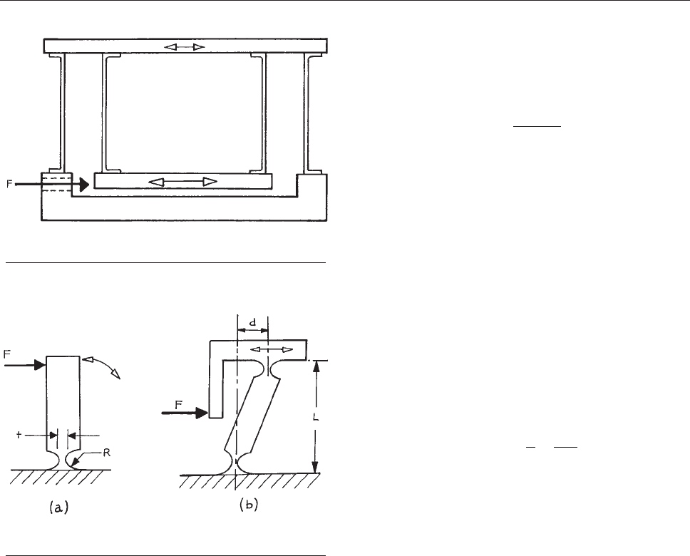
near the clamped end of a spring is quite similar to what
would occur when a bending moment is applied to a
cantilever that is notched near its fixed end, as shown in
Figure 1.65(a). This is a notch
hinge. A beam with a notch
hinge at each end can simulate a leaf spring fixed at one
end to a base and at the other end to a transversely moving
platform. The obvious extension of this idea is a flexure in
which the base, platform, and spring are all machined from
a single piece of material. Figure 1.65(b) shows the mono-
lithic
notch-hinge analogy to the basic linear-motion flex-
ure illustrated in Figure 1.62(b) . The force–displacement
relation
for the notch hinge has been derived analytically
by Paros and Weisbord
13
and by finite element methods
by Smith, Chetwynd, and Bowen.
14
The latter analysis
gives:
d ¼
3FKRL
2
EBt
3
ð1:41Þ
for the basic linear-motion flexure illustrated in
Figure 1.65(b),whereR i
s the radius of each of the notches,
t is the width of the web at each notch, B is the width of the
beam (as in Figure 1.48), and the factor K ac
counts for the
effective length of the flexible part of the web. K varies from
about 0.2 for a relatively thin, flexible web, where t is much
less than R, to about 0.7 for a relatively stiff spring, with t
comparable to R.
Flexures provide for relatively small displacements,
especially flexures employing notch hinges. Linear
force–displacement response, free of hysteresis, requires
that the elastic limit of the spring material not be exceeded.
For the linear-motion notch-hinge flexure in Figure 1.65(b),
maximum
displacement, in the model of Smith, et al.,
14
is
approximated by:
d
max
¼ 4K
R
t
s
max
E
L ð1:42Þ
where s
max
is the maximum tolerable stress in the material
of the spring. For design purposes, s
max
can be taken to be
the yield strength of the material, or, conservatively, some
fraction thereof. The ratio of the yield strength to the mod-
ulus of elasticity (E) for mild steel, stainless steel, or tem-
pered aluminum alloy is about 0.003 and for hard plastics
such as polyamide (Nylon) or polyimide (Vespel) the ratio
is about 0.03. In a simple notch-hinge linear-motion
flexure, the ratio (R/t) is typically about 5; this gives a
maximum displacement of no more than about 0.01L for
a simple metal flexure and 0.1L for a plastic flexure.
As s ugg ested by the cont our of the notch hinges shown
in Figure 1.65, fabri cation of a monolithic flexure
requi
res only milling a nd bori ng operations. The preci-
sion of the motion, as well as the stiffness, of a monolithic
flexure is determined primarily by the precision in the
location of the centers of t he holes that create a notch.
The relative ease of manufacture of precise monolithic
flexures allows for q uite complex designs. An elegant,
Figure 1.64 A compound flexure design to correct for the
error shown in Figure 1.63.
Figure 1.65 Monolithic flexures analogous to those shown
in Figure 1.62.
CONSTRAINED MOTION 65
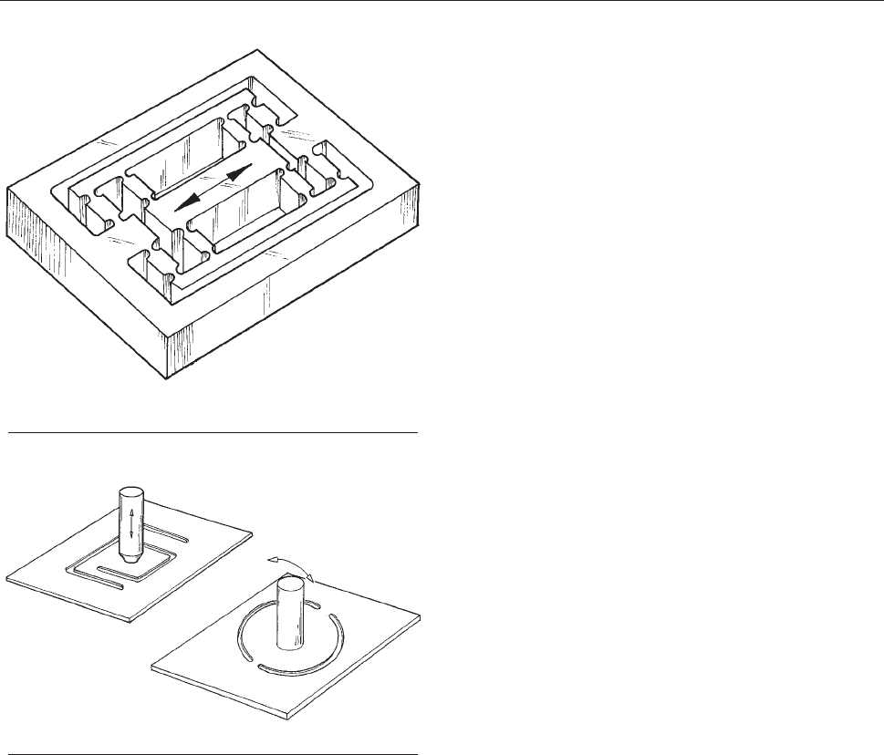
stable, and precise, double-c om pound, recti linear sprin g
designed by Smith, et al.,
14
is shown in Figure 1.66.
There are many variations on the basic notch spring. On
a beam, a closely spaced pair of notches at right angles
provides for two degrees of freedom. Notch springs
machined into thin metal stock can serve the function of
a Belleville spring to absorb shock or take up end-play in a
mechanism or to limit motion to a single plane. Examples
are shown in Figure 1.67. In these flexures the material in
the
notch is stressed in torsion.
Cited References
1. R. P. Pohandish (Ed.), Machinery’s Handbook
Pocket Companion, Industrial Press Inc., New York, 2000.
2. ASM Handbook Volume 04: Heat Treating, ASM
International, Ohio, 1991.
3. J. W. Dally and W. F. Riley, Experimental Stress Analysis,
McGraw-Hill, New York, 1965, pp. 165–221.
4. F. Rosebury, Handbook of Electron Tube and Vacuum
Techniques, Addison-Wesley, Reading, MA, 1965.
5. A comprehensive list of brazing alloys has been compiled
by W. H. Kohl, in Handbook of Vacuum Physics, Vol. 3,
Technology, A. H. Beck (Ed.), Pergamon Press, Elmsford,
NY, 1964; Materials and Techniques for Electron Tubes,
Reinhold, N, 1959. See also reference 6.
6. The Brazing Book, Lucas-Milhaupt/Handy & Harman of
Canada, Cudahy, WI, USA.
7. R. J. Roark, Formulas for Stress and Strain, 4th edn.,
McGraw-Hill, New York, 1965.
8. C. Mathews, A. S. M. E. Engineer’s Data Book, 2nd edn.,
ASME Press, NY, 2001, pp. 75, 188–189.
9. D. E. Newland, Mechanical Vibration Analysis and
Computation, Longman Scientific & Technical/John Wiley
& Sons, Inc., New York, 1989; S. S. Rao, Mechanical
Vibrations, 2nd edn., Addison-Wesley, Reading, MA, 1990;
W. Weaver, Jr., S. P. Timoshenko, and D. H. Young,
Vibration Problems in Engineering, 5th edn., John
Wiley & Sons, Inc., New York, 1990.
10. A useful review of kinematic design is given by J. E. Furse,
J. Phys. E., 14, 264, 1981.
11. S. T. Smith and D. G. Chetwynd, Foundations of
Ultraprecision Mechanism Design, Gordan and Breach
Science Publishers, Philadelphia, 1992.
12. R. V. Jones, J. Sci. Instr ., 28, 38, 1951; J. Sci. Instr ., 33,
11, 1956.
13. J. M. Paros and L. Weisbord, Machine Design, 151, 25 Nov.
1965.
14. S. T. Smith, D. G. Chetwynd, and D. K. Bowen, J. Phys.
E: Sci. Instrum., 20, 977, 1987.
General References
Design of Moving and Rotating
Machinery
R. M. Phelan, Dynamics of Machinery, McGraw-Hill, New York,
1967.
Figure 1.66 Monolithic, double-compound, rectilinear
spring (reference 14).
Figure 1.67 Monolithic flexures in a thin material.
66 MECHANICAL DESIGN AND FABRICATION

Vibration Analysis
D. E. Newland, Mechanical Vibration Analysis and Computation,
5th edn., Longman Scientific & Technical, Essex, England and
John Wiley & Sons, New York, 1989.
S. S. Rao, Mechanical Vibrations, 2nd edn., Addison-Wesley,
Reading, MA, 1990.
W. Weaver, Jr., S. P. Timoshenko, and D. H. Young,
Vibration Problems in Engineering, John Wiley & Sons,
New York, 1990.
Mechanical Design Texts
A. D. Deutschman, W. J. Michels, and C. E. Wilson, Machine
Design, Macmillan, New York, 1975.
V. M. Faires, Design of Machine Elements, 4th edn., Macmillan,
New York, 1965.
R. E. Parr, Principles of Mechanical Design , McGraw-Hill,
New York, 1970.
R. M. Phelan, Fundamentals of Mechanical Design, 3rd edn.,
McGraw-Hill, New York, 1970.
S. T. Smith and D. G. Chetwynd, Foundations of Ultraprecision
Mechanism Design, Gordan and Breach Science Publishers,
Philadelphia, 1992.
Mechanical-Drawing Texts
T. E. French and C . J. Vierck, Engineering Drawing and
Graphic Technology,11thedn.,McGraw-Hill,NewYork,
1972; (entitled A Manual of Enginee ring Drawing in its first
10 editions).
F. E. Ciesecke, A. Mitchell, H. C. Spencer, and I. L. Hill,
Technical Drawing, 5th edn., Macmillan, New York, 1967.
Mechanical Engineering Handbooks
R. Timings, Mechanical Engineer’s Pocket Book, 3rd edn.,
Newnes/Elsevier, Oxford, 2006.
R. P. Pohandish (Ed.), Machinery’s Handbook Pocket Companion,
Industrial Press Inc., New York, 2000.
C. Mathews, A. S. M. E. Engineer’s Data Book, 2nd edn., ASME
Press, NY, 2001.
Properties of Materials
A. J. Moses, The Practicing Scientist’s Handbook, Van Nostrand
Reinhold, New York, 1978; F. Rosebury, Handbook of Electron
Tube and Vacuum Techniques, Addison-Wesley, Reading,
MA, 1965.
Goodfellow Catalog, Berwyn, PA and, Goodfellow
Cambridge Limited, Cambridge, web catalog http://
www.goodfellow.com.
Brazing
The Brazing Book, Lucas-Milhaupt/Handy & Harman
of Canada, Cudahy, WI and online at http://www.
handyharmancanada.com
REFERENCES 67

Appendix 1.1 Number drills with inch and metric
equivalents and tap sizes for approximately 75% thread
depth.
SIZE No
or Letter
inches mm Tap Size
American
National
Tap Size ISO
Metric Coarse
Thread Series
80 .0135 0.34
79 .0145 0.37
78 .0160 0.41
77 .0180 0.46
76 .0200 0.51
75 .0210 0.53
74 .0225 0.57
73 .0240 0.61
72 .0250 0.64
71 .0260 0.66
70 .0280 0.71
69 .0292 0.74
0.75 M1
68 .0310 0.79
67 .0320 0.81
66 .0330 0.84
65 .0350 0.89
64 .0360 0.91
63 .0370 0.94
0.95 M1.2
62 .0380 0.97
61 .0390 0.99
60 .0400 1.02
59 .0410 1.04
58 .0420 1.07
57 .0430 1.09
1.15 M1.4
56 .0465 1.18
3/64 0-80
1.30 M1.6
55 .0520 1.32
54 .0550 1.40
1.50 M1.8
53 .0595 1.51 1-64
52 .0635 1.61
1.65 M2
51 .0670 1.70
50 .0700 1.78 2-56
1.8 M2.2
49 .0730 1.85
48 .0760 1.93
47 .0785 1.99 3-48
68 MECHANICAL DESIGN AND FABRICATION

Appendix 1.1. (contd.)
SIZE No
or Letter
inches mm Tap Size
American
National
Tap Size ISO
Metric Coarse
Thread Series
46 .0810 2.06
45 .0820 2.08
2.10 M2.5
44 .0860 2.18
43 .0890 2.26 4-40
42 .0935 2.37
41 .0960 2.44
40 .0980 2.49
39 .0995 2.53
2.55 M3
38 .1015 2.58 5-40
37 .1040 2.64
36 .1065 2.71 6-32
35 .1100 2.79
34 .1110 2.82
33 .1130 2.87
32 .1160 2.95 M3.5
31 .1200 3.05
30 .1285 3.26
3.40 M4
29 .1360 3.45 8-32
28 .1405 3.57
27 .1440 3.66
26 .1470 3.73
25 .1495 3.80 10-24 M4.5
24 .1520 3.86
23 .1540 3.91
22 .1570 3.99
21 .1590 4.04 10-32
20 .1610 4.09
19 .1660 4.22
4.30 M5
18 .1695 4.31
17 .1730 4.39
16 .1770 4.50 12-24
15 .1800 4.57
14 .1820 4.62
13 .1850 4.70
12 .1890 4.80
11 .1910 4.85
10 .1935 4.91
9 .1960 4.98
8 .1990 5.05
APPENDIX 69

Appendix 1.1. (contd.)
SIZE No
or Letter
inches mm Tap Size
American
National
Tap Size ISO
Metric Coarse
Thread Series
5.10 M6
7 .2010 5.11 1/4-20
6 .2040 5.18
5 .2055 5.22
4 .2090 5.31
3 .2130 5.41 1/4-28
2 .2210 5.61
1 .2280 5.79
A .234 5.94
B .238 6.05
6.10 M7
C .242 6.15
D .246 6.25
E .250 6.35
F .257 6.53 5/16-18
G .261 6.63
H .266 6.76
6.90 M8
I .272 6.91
J .277 7.04
K .281 7.14
L .290 7.37
M .295 7.49
N .302 7.67
7.90 M9
5/16 3/8-16
O .316 8.03
P .323 8.20
Q .332 8.43
8.60 M10
R .339 8.61
S .348 8.84
T .358 9.09
U .368 9.35 7/16-14
V .377 9.58
9.60 M11
W .386 9.80
X .397 10.08
Y .404 10.26
10.40 M12
Z .413 10.49
27/64 1/2-13
29/64 1/2-20
.480 12.20 M14
70 MECHANICAL DESIGN AND FABRICATION

Appendix 1.3 ISO (Metric) Coarse Threads.
Size
M(mm)
Pitch
(mm)
Tap Drill
(mm)
Size
M(mm)
Pitch
(mm)
Tap Drill
(mm)
M1 0.25 0.75 M3.5 0.6 2.90
M1.2 0.25 0.95 4 0.7 3.30
M1.4 0.30 1.10 5 0.8 4.20
M1.6 0.35 1.25 6 1 5.00
M1.8 0.35 1.45 8 1.25 6.80
M2 0.4 1.60 10 1.5 8.50
M2.2 0.45 1.75 12 1.75 10.50
M2.5 0.45 2.05 14 2 12.00
M3 0.5 2.50 16 2 14.00
M3.5 0.6 2.90 18 2.5 15.50
Appendix 1.2 American Standard Threads. Unified National Coarse (UNC) and
Unified National Fine (UNF) threads with tap drill and clearance drill sizes.
The tap drill size is for approximately 75% thread depth. A range of
clearance hole drills is given depending upon whether a close fit
or a free fit is desired.
(Number and letter drill diameters are given in Appendix 1.1.)
Size
(Nominal
Diameter,
Inches)
UNC UNF Clearance
Hole Drill
Close-Free
Threads
per Inch
Tap Drill
Size
Threads
per Inch
Tap Drill
Size
0 (0.060) 80 3/64 52–50
1 (0.073) 64 53 72 53 48–46
2 (0.086) 56 50 64 50 43–41
3 (0.099) 48 47 56 45 37–33
4 (0.112) 40 43 48 42 32–30
5 (0.125) 40 38 44 37 30–29
6 (0.138) 32 36 40 33 27–25
8 (0.164) 32 29 36 29 18–16
10 (0.190) 24 25 32 21 9–7
12 (0.216) 24 16 28 14 2–1
1/4 20 7 28 3 F–H
5/16 18 F 24 I P–Q
3/8 16 5/16 24 Q W–X
7/16 14 U 20 25/64 29/64–15–32
1/2 13 27/64 20 29/64 33/64–17/32
Note: ASA B1.1-1989.
APPENDIX 71

Appendix 1.5 British Standard Pipe Thread Tapered.
(BSPT, BS EN 10226 equivalent to ISO 7)
Nominal
Bore Size
of Pipe
a
(in.)
Nominal
Bore Size of
Pipe
a
(mm)
Pipe
OD
(mm)
Threads
per
Inch
Pitch
(mm)
Length of
Engagement
by Hand
(mm)
Effective
Thread
Length
(mm)
1/8 6 10.2 28 0.907 4.0 6.5
1/4 8 13.5 19 1.337 5.0 8.7
3/8 10 17.5 19 1.337 6.4 10.1
1/2 15 21.3 14 1.814 8.2 13.2
3/4 20 26.9 14 1.814 9.5 14.5
1 25 33.7 11 2.309 10.4 16.8
11/4 32 42.4 11 2.309 12.7 19.1
11/2 40 48.3 11 2.309 12.7 19.1
a
Nominal bore sizes in inches and mm are equivalents not conversions
Appendix 1.4 American Standard Taper Pipe Threads.
Nominal Bore
Size of Pipe
(in.)
Actual O.D.
of Pipe
(in.)
Threads
per Inch
Length of
Engagement
by Hand
(in.)
Length of
Effective
Thread
(in.)
1/8 0.405 27 0.180 0.260
1/4 0.540 18 0.200 0.401
3/8 0.675 18 0.240 0.408
1/2 0.840 14 0.320 0.534
3/4 1.050 14 0.340 0.546
1 1.315 11 1/2 0.400 0.682
11/4 1.660 11 1/2 0.420 0.707
11/2 1.900 11 1/2 0.420 0.724
2 2.375 11 1/2 0.436 0.756
21/2 2.875 8 0.682 1.136
3 3.500 8 0.766 1.200
Note: ASA B2.1-1989.
72 MECHANICAL DESIGN AND FABRICATION
Appendix 1.6 CGA connections for high-pressure gas cylinders.
CGA 110
.3125-32UNEF-2B-RH-INT
CGA 165
.4375-20UNF-2A-RH-EXT (1⁄4" SAE Flare)
CGA 180
.625-18UNF-2A-RH-EXT
CGA 240
.375-18NGT-RH-INT
CGA 280
.745-14NGO-RH-EXT
CGA 290
.745-14NGO-LH-EXT
CGA 295
.750-16UNF-2A-RH-EXT (1⁄2" SAE Flare)
CGA 296
.803-14UNS-2B-RH-INT
CGA 320
.825-14NGO-RH-EXT (Flat Nipple)
CGA 326
.825-14NGO-RH-EXT (Small Round Nipple)
CGA 330
.825-14NGO-LH-EXT (Flat Nipple)
CGA 346
.825-14NGO-RH-EXT (Large Round Nipple)
CGA 347
.825-14NGO-RH-EXT (Long Round Nipple)
CGA 350
.825-14NGO-LH-EXT (Round Nipple)
CGA 170
.5625-18UNF-2A-RH-EXT
Washer or O-Ring
may be used
APPENDIX 73
CGA 500
.885-14NGO-RH-INT (Bullet Nipple)
CGA 510
.885-14NGO-LH-INT (Bullet Nipple)
CGA 540
.903-14NGO-RH-EXT
CGA 555
.903-14NGO-LH-EXT
CGA 580
.965-14NGO-RH-INT
CGA 590
.965-14NGO-LH-INT
CGA 660
1.030-14NGO-RH-EXT (Face Washer)
CGA 670
1.030-14NGO-LH-EXT (Face Washer)
CGA 677
1.030-14NGO-LH-EXT (Round Nipple)
CGA 678
1.030-14NGO-LH-EXT (Recessed Washer)
CGA 679
1.030-14NGO-LH-EXT (Tipped Nipple)
CGA 680
1.045-14NGO-RH-INT
CGA 695
1.045-14NGO-LH-INT
CGA 701
1.103-14NGO-RH-EXT
CGA 440
.875-14UNF-2A-RH-EXT (5⁄8" SAE Flare)
Appendix 1.6 (contd.)
74 MECHANICAL DESIGN AND FABRICATION
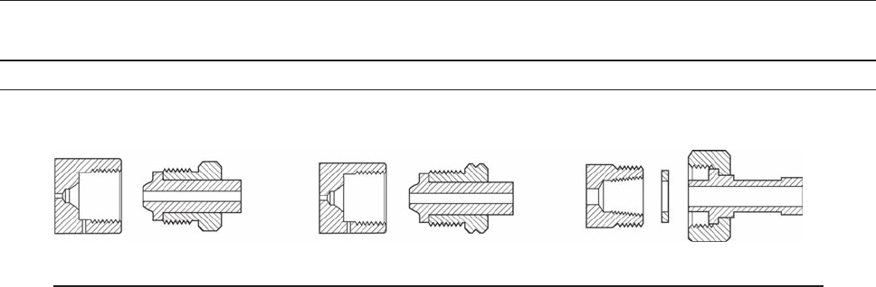
CGA 702
1.125-14NGO-RH-INT
CGA 703
1.125-14NGO-LH-INT
CGA 705
1.125-14UNS-2A-RH-EXT
Appendix 1.6 (contd.)
APPENDIX 75

WORKING WITH GLASS
Glass has been called the miraculous material. The ubiq-
uity of glass in the modern laboratory certainly confirms
this. Because glass is chemically inert, most containers are
made of it. Glass is transparent to many forms of radiation,
and its transmission properties can be varied by controlling
its composition; all sorts of windows and lenses are made
of glass. Because glass can be polished to a high degree
and is dimensionally stable, most mirrors are supported on
glass surfaces. Glass is strong and stiff, and is often used as
a structural material. Considering its mechanical rigidity
and density, it is a reasonably good thermal insulator. It is
an excellent electrical insulator. Perhaps the greatest virtue
of this material is that many glasses are inexpensive and
can be cut and shaped in the laboratory with inexpensive
tools.
Fifty years ago, most glass laboratory apparatus was
produced by the scientist or technician in situ by blowing
molten glass or by grinding, cutting, and polishing hard
glass. Today the glass industry has grown to such an extent
that nearly all components of a glass apparatus are available
from commercial sources at low cost. These include all sorts
of containers, chemical labware, vacuum-system compo-
nents, mirrors, windows, and lenses. It is often only neces-
sary for laboratory scientists to acquaint themselves with the
range of components available and to acquire the skills
needed to assemble an apparatus from these components.
2.1 PROPERTIES OF GLASSES
The chemical composition of glass is infinitely variable,
and so therefore are the thermal, electrical, mechanical,
and chemical properties of glass. Furthermore, glass is a
fluid that retains a memory of its past history. It is possible,
however, to review the general properties of glass and to
specify the properties of glasses of a particular composi-
tion and method of manufacture.
2.1.1 Chemical Composition and Chemical
Properties of Some Laboratory
Glasses
The chief constituent of any commercial glass is silica
(SiO
2
). All laboratory ware is at least 3/4 silica, with other
oxides added to obtain certain thermal properties or chem-
ical resistance.
The least expensive and, until the last quarter century,
the most common glass used for laboratory ware is known
as soda-lime glass or soft glass. This glass contains 70–
80% silica, 5–10% soda (Na
2
O), 5–10% potash (K
2
O), and
10% lime (CaO). A particular advantage of this glass is
that it can be softened in a natural-gas–air flame.
Borosilicate glass has supplanted soda-lime glass for the
manufacture of labware. In this glass the alkali found in
soft glass is replaced by B
2
O
3
and alumina (Al
2
O
3
). Boro-
silicate glass is superior to soda-lime glass in its resistance
to chemical attack and thermal or mechanical shock. It
softens at a higher temperature than soft glass, however,
and is more difficult to work. Borosilicate glasses of many
different compositions are manufactured for various labo-
ratory applications, but far and away the most common
laboratory glass is the borosilicate glass designated by
Corning as Pyrex 7740 and by Kimble as Kimax KG-33.
The composition is: SiO
2
, 80.5%; B
2
O
3
, 12.9%; Na
2
O,
76
CHAPTER
2

3.8%; Al
2
O
3
, 2.2%; K
2
O, 0.4%. Borosilicate glass tubing
and rod, as well as a wide range of components, are avail-
able from many suppliers, including Corning Glass Works,
Kimble-Kontes, Wilmad-Labglass, ChemGlass, and Ace
Glass.
Glassware of extremely good chemical resistance is pro-
duced from borosilicate glass by thermal and chemical
processing: a heat treatment causes the glass to separate
into two phases – one high in silica and the other rich in
alkali and boric oxides. This second phase is leached out
with acid, and the remaining phase is heated to give a clear
consolidated glass that is nearly pure silica. This glass is
known as 96% silica glass and is designated by Corning as
Vycor No. 7900.
Glass composed only of silica is known as vitreous or
fused silica or simply as ‘‘quartz.’’ Because of its refrac-
tory properties and chemical durability, this material
would be the most desirable glass were it not for the high
cost of making it and the extremely high temperatures
required to work it. On the other hand, the relative cost
of quartz is decreasing to the extent that the market for
96% silica glass is rapidly disappearing.
Most laboratory glasses are transparent to visible light,
making visual distinction between the various glass com-
positions impossible. For this reason it is important to label
glass materials before storing and to avoid mixing different
kinds of glass. When necessary it is possible to distinguish
different glasses from one another by differences in ther-
mal or optical properties. The gas–air flame of a Bunsen
burner will soften soda-lime glass, but not borosilicate
glass. A natural-gas–oxygen flame is required to soften
borosilicate glass, but this flame will not affect fused silica.
Fused silica must be raised to a white heat in an oxyhy-
drogen flame before it will soften. Glasses of different
composition cannot generally be successfully fused
together because of differences in the amount of expansion
and contraction on heating and cooling. An unknown piece
of glass may be compared with a known piece by placing
the two side by side with their ends coincident. The two
ends are softened together in a flame and pressed together
with tweezers. Then the fused ends are reheated and drawn
out into a long fiber about 0.5 mm in diameter and permit-
ted to cool. If the fiber remains straight, the two pieces
have the same coefficient of expansion. If the fiber curves,
the two pieces are of different composition.
A measurement of the refractive index is usually a sen-
sitive and reliable test of glass composition. A piece of
glass placed in a liquid of exactly the same refractive index
will become invisible. For example, a test solution for
Pyrex 7740 can be made of 16 parts by volume of methanol
in 84 parts benzene. This test solution should be kept in a
tightly covered container so that its composition does not
change as a result of evaporation.
As can be judged from the extreme chemical environ-
ments to which glasses are routinely subjected, glass is
indeed resistant to chemical action. However, one need
only observe windows clouded by the action of rainfall
in a polluted atmosphere or glassware permanently stained
by laboratory chemicals to confirm that glass is not entirely
impervious to chemical attack. Glass is attacked most
readily by alkaline solutions, and all types are affected
about equally. Water has an effect. The soft glasses are
most susceptible, borosilicate glass is only slightly
affected, and 96% silica hardly at all, since most of its
soluble components were leached out in manufacture.
Acids attack glass more readily than water, although,
again, borosilicate glass is more resistant to acids than soda
glass, and 96% silica is more resistant yet.
2.1.2 Thermal Properties of
Laboratory Glasses
One of t he most important pro perties of glass is its very
low coefficient of therm al expansi on. It is this property
thatpermitsglasstobeformedathightemperaturesina
molten state and then cooled without changing shape or
breaki ng. The coe fficient s of linear expansion of several
types of glass are given in Table 2.1. As can be seen from
th
ese data, borosilicate glass is much more resistant to
thermal shock than soft glass. Fused s ilica is so stable that
a white-hot piece can be immersed in liquid air without
fracturing.
Glass does not have a melting point. Instead, the work-
ing properties of a glass are specified by particular points
on its viscosity–temperature curve. The softening point is
approximately the temperature at which a glass can be
observed to flow under its own weight. The annealing
point is the temperature at which internal stresses can be
relieved (annealed) in a few minutes. The strain point is
the temperature below which glass can be quickly cooled
PROPERTIES OF GLASSES 77

without introducing additional stress. The working point is
the temperature at which the glass is formed by a skilled
glassblower.
The specific heat of glass is about 0.8 J g
1
K
1
, and the
thermal conductivity of glass is about 0.008 J cm sec
1
cm
2
K
1
. For reference, this thermal conductivity is
about an order of magnitude less than that of graphite,
two orders less than that of metal, and about an order of
magnitude greater than that of wood.
2.1.3 Optical Properties of Laboratory
Glassware
In many experiments light must be transmitted through the
wall of a glass container. The transmission as a function of
wavelength depends upon the composition of the glass.
The composition of the soda-lime glasses varies consider-
ably, and the optical properties of each piece should be
determined by spectroscopic analysis before it is used in
an experiment requiring light transmission. Spectrophoto-
metric curves for some lab glasses of well-defined compo-
sition are given in Figure 2.1. As can be seen, fused silica is
transparent
over the widest wavelength range.
2.1.4 Mechanical Properties of Glass
The tensile, compressive, and shear strength of a piece of
glass depends upon its shape and history and upon the time
over which it is loaded. Glass appears to be much stronger
in compression than tension. This is in part due to the fact
that a glass surface can be made very smooth in order
to uniformly distribute a compressive load. Values of
400–1200 MN/m
2
(60 000–180 000 psi) are quoted for
the compression strength. (1 psi (pound per square inch) ¼
6895 N/m
2
.)
Glass is nearly perfectly elastic. When it breaks it does
so without plastic deformation. Springs made of glass or
quartz fibers behave almost ideally. The modulus of
elasticity of glass is high and, of course, depends upon
composition. Young’s modulus (the modulus of elasticity)
for Pyrex 7740 is 63 GN m
2
(9.1 3 10
6
psi) at 0 °C and
65 GN m
2
(9.4 3 10
6
psi) at 100 °C. For fused silica the
corresponding values are 72 GN m
2
(10.5 3 10
6
psi) and
74 GN m
2
(10.7 3 10
6
psi).
Glass fibers are very strong. A quartz fiber 0.3 mm (.01 in.)
in diameterhas a tensile strength of 0.3 GN m
2
(50 000 psi);
a fiber 0.03 mm (.001 in.) in diameter a strength of at least
1.3 GN m
2
(200 000 psi); and a fiber 0.003 mm (.0001 in.)
in diameter a strength in excess of 7 GN m
2
(1 000 000 psi).
2.2 LABORATORY COMPONENTS
AVAILABLE IN GLASS
The list of laboratory apparatus components produced com-
mercially in glass is nearly endless. The laboratory scientist
should make a careful survey of lab suppliers’ literature
before embarking on the design and construction of a glass
apparatus. Very often a complex device can be assembled
in the lab entirely from inexpensive components without
requiring the services of a skilled glassblower. Some of
the most frequently used glass components are described
below.
2.2.1 Tubing and Rod
Most laboratory supply houses carry a wide range of tub-
ing and rod of Pyrex 7740 or Kimax KG-33 in 1 m lengths
at a cost of only a few euros per kilogram. Outer diameters
Table 2.1 Thermal properties of glass
Glass Linear Expansion
Coefficient (cm
1
K
1
)
Strain Point
(°C)
Annealing Point
(°C)
Softening Point
(°C)
Working Point
(°C)
Soda-lime (typical) 8–10 3 10
6
500 550 700 1000
Pyrex 7740 (borosilicate) 3.3 3 10
6
510 555 820 1250
Vycor 7900 (96% silica) 0.75 3 10
6
890 1020 1500 —
Fused Silica 0.55 3 10
6
950 1100 1600 —
78 WORKING WITH GLASS
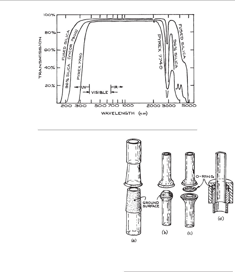
between 3 and 178 mm are readily available. The standard
wall thickness ranges from 0.5 mm for the smallest tubing
to 3.5 mm for the largest. Heavy-wall tubing with wall
thickness ranging from 2 to 10 mm is also available. In
addition, heavy-wall tubing of very small bore diameter
(0.5–4 mm), known as capillary tubing, is available.
Finally, solid rod of 3 to 30 mm diameter is a standard
item.
2.2.2 Demountable Joints
Laboratory apparatus can be quickly assembled if compo-
nents are connected with joints of the type illustrated in
Figure 2.2.
A
gas- or liquid-tight seal between two close-fitting
pieces of glass can be achieved if the mating surfaces are
lightly coated with a viscous lubricant before assembly. A
number of low-vapor-pressure lubricants such as Apiezon
vacuum grease or Dow-Corning silicone vacuum grease
are especially formulated for this purpose. The taper joint
and the ball-and-socket joint in Figure 2.2(a) and (b) are
assembled
in this manner. The mating surfaces must fit
together very well. In general this requires that they be
Figure 2.2 Demountable joints: (a) standard-taper joint;
(b) ball-and-socket joint; (c) O-ring joint; (d) a quick-connect
joint. (a), (b), and (c) are used for attaching glass compo-
nents to one another; (d) is used for joining a glass tube to a
metal component.
Figure 2.1 Optical-transmission curves for Pyrex 7740, Vycor 7900 (96% silica), and
fused silica.
LABORATORY COMPONENTS IN GLASS 79
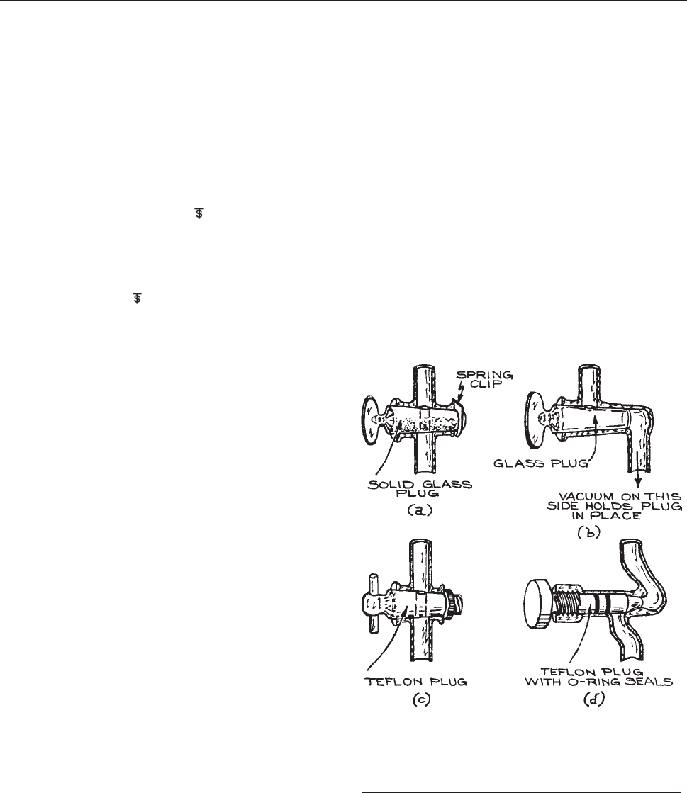
lapped together. This is accomplished by coating the sur-
faces with a fine abrasive such as Carborundum in water,
fitting the pieces together, and rotating one with respect to
the other. The rotation should not be continuous, but rather
after half a turn or so the pieces should be pulled apart and
then assembled again so as to redistribute the abrasive.
Fortunately, taper and ball-and-socket joints with ground
mating surfaces are now commercially produced in stand-
ard sizes with sufficient precision that lapping and grinding
in the lab is seldom necessary.
The standard taper (indicated
) for ground joints is
1:10. Standard-taper joints on tubing with outer diameters
between 8 and 50 mm are available. These joints are iden-
tified by figures that indicate the diameter of the large end
of the taper and the length of the ground zone in milli-
meters. For example,
10/30 indicates a ground zone
10 mm in diameter at the large end and 30 mm in length.
Standard-taper ground joints are available in borosilicate
glass, quartz, and type-303 stainless steel. These compo-
nents are interchangeable, and thus it is often convenient
to make a transition from glass to quartz or from glass to
metal with a taper joint.
Ball-and-socket ground joints do not seal as reliably as
taper joints; however, their design p erm its misalignment
and even some slight motion between joined parts. This
type of joint must be secured with a suitable clamp. Ball-
and-socket joints are designated by a two-number code
(i.e., 28/15). The first number gives the diameter of the
ball in millimeters, the second number the inner diameter
of the tubing to which the ball and socket are attached.
Ball-and-socket joints of standard sizes are commer-
cially available in borosilicate glass, quartz, and stainless
steel.
The O-ring joint illustrated in Figure 2.2(c) is rapidly
replacing
the ground joint as a means of making demount-
able joints in glass vacuum apparatus. These joints require
no grease. Furthermore, the mating pieces are sexless,
since each member of the joint is grooved to a depth of
less than half the thickness of the O-ring. To date, these
joints are only available in borosilicate glass.
Quick-connects of the type shown in Figure 2.2(d) are
also
sealed with an O-ring. They are suited to joining either
glass or metal tubing to a metal container. Quick-connects
are often used to join glass ion-gauge tubes to metal vac-
uum apparatus.
2.2.3 Valves and Stopcocks
A glass stopcock of one of the types illustrated in Figures
2.3(a)–(c) has traditionally been used for control ling fluid
flo
w in glass apparat us. These c onsist of a hollow tapered
body and a plug with a hole bored through that can be
aligned by rotation with inlet and outlet ports in the body.
The simplest and least expensive version uses a glass plug
with a ground surface that mates with a ground surface on
the interior o f the stopcock body. The surf ace of the plug
must be lightly lubricated with stopcock grease to ensure
a good seal a nd f ree do m of r ota tio n. A stopcock of th is
typemaybeusedtocontrolliquidfloworgasflowat
pressures down to a few millitorr. For use at pressur es
above 1 atm the end of the plug may be fitted with a
spring-loaded clip or collar to prevent i ts being blown
out. Stopcocks of this type are now available with a
Teflon plug. These are well suited for use with liquids.
Figure 2.3 Stopcocks and valves for controlling fluid flow:
(a) glass stopcock with solid glass plug; (b) high-vacuum
stopcock with vacuum cup and hollow plug; (c) glass stop-
cock with Teflon plug; (d) threaded glass vacuum valve with
O-ring-sealed Teflon stem.
80 WORKING WITH GLASS

No lubrication is required, and the plug seldom freez es in
the body of the stopcock.
In glass vacuum systems, the stopcock illustrated in
Figure 2.3(b) is far more reliable than the simple solid plug
design.
The plug is hollow, and the small end of the body is
closed off by a vacuum cup so that the interior of the
stopcock can be evacuated. The plug is held securely in
place by atmospheric pressure.
Valves with threaded borosilicate glass bodies and
threaded Teflon plugs [Figure 2.3(d)] are rapidly replacing
con
ventional stopcocks for most applications. These
valves are no more expensive than good vacuum stop-
cocks. They require no lubrication; only glass and Teflon
are exposed to the interior of the system. They are suitable
for use with most liquids and gases and may be used at
pressures from 10
6
torr to 15 atm.
2.2.4 Graded Glass Seals and
Glass-to-Metal Seals
In general, glasses of dif ferent composition hav e different
coefficients of thermal expansion. As a consequence, two
glasses of dif ferent composition usually cannot be joined,
since differing rates of expansion and contraction produce
destructive stresses as the fused joint cools. In practice two
glasses can be successfully joined if their coef ficients of ther -
mal expansion differ by no more than about 1 3 10
6
K
1
.
The problem of joining two glasses with significantly differ-
ent coefficients of thermal expansionis solvedby interposing
several layers of glass, each with a coefficient only slightly
different from its neighbors. This stack of glass when fused
together is called a graded seal. Tubing with graded seals
joining different glasses is manufactured commercially.
Borosilicate-to-soft-glass seals are available in tube
sizes from 7 to 20 mm. Seals graded from borosilicate
glass (for example Pyrex 7740) to quartz (Vycor 7913)
are available in tube sizes from 7 to 51 mm.
Glass tubing can, with care, be joined to metal tubing.
Ideally the glass and the metal should have the same coef-
ficient of expansion. It has been demonstrated, however,
that glass tubing can be joined to metal tubing that has a
very different coefficient provided that the end of the metal
tubing has been machined to a thin, sharp, feathered edge.
1
The stresses of thermal expansion and contraction can then
be taken up by stretching of the metal. The stresses created
by joining glass to metal can also be reduced by interpos-
ing glasses whose coefficient of thermal expansion is inter-
mediate between that of the metal and the final glass.
Direct tube seals between borosilicate glass and copper
or stainless steel are available in diameters from 6 mm to
50 mm. Graded glass seals between borosilicate glass and
Kovar, an iron–nickel–cobalt alloy, are available in sizes
from 3 mm to 75 mm. These graded seals are robust, and
far and away the most common glass-to-metal seal. Kovar is
easily silver-soldered or welded to most steels and brasses.
2.3 LABORATORY GLASSBLOWING
SKILLS*
Considering the range of components now available, it is
usually only necessary for the laboratory worker to be able
to join commercially produced components to assemble a
complete apparatus. The required skills consist primarily
of joining tubes in series or at right angles, cutting and
sealing-off tubing, and making simple bends. It is easiest
and often necessary to make a joint between a piece of
tubing held in the hand and a piece attached to an apparatus
or otherwise rigidly clamped. In the following sections
only the simplest glassblowing operations with borosili-
cate glass are described. There are certainly many more
elegant and complex manipulations that can be carried out
by a skilled glassblower using only hand tools. Workers
who find a need for these operations or discover in them-
selves a flair for glassblowing may consult a more com-
plete text on the subject.
2.3.1 The Glassblower’s Tools
The necessary equipment for laboratory glasswork is illus-
trated in Figure 2.4. The basic tool is, of course, a torch.
The
National type-3A blowpipe with #2, #3, or #4 tip is the
standard in the trade. A torch stand is essential to hold the
lighted torch when both hands are required to manipulate a
piece of glass. A source of natural gas and low-pressure
* Many of the simplified methods described in Section 2.3 were devel-
oped by John Trembly at the University of Maryland for use in his
remarkably successful introductory glassblowing classes.
LABORATORY GLASSBLOWING SKILLS 81
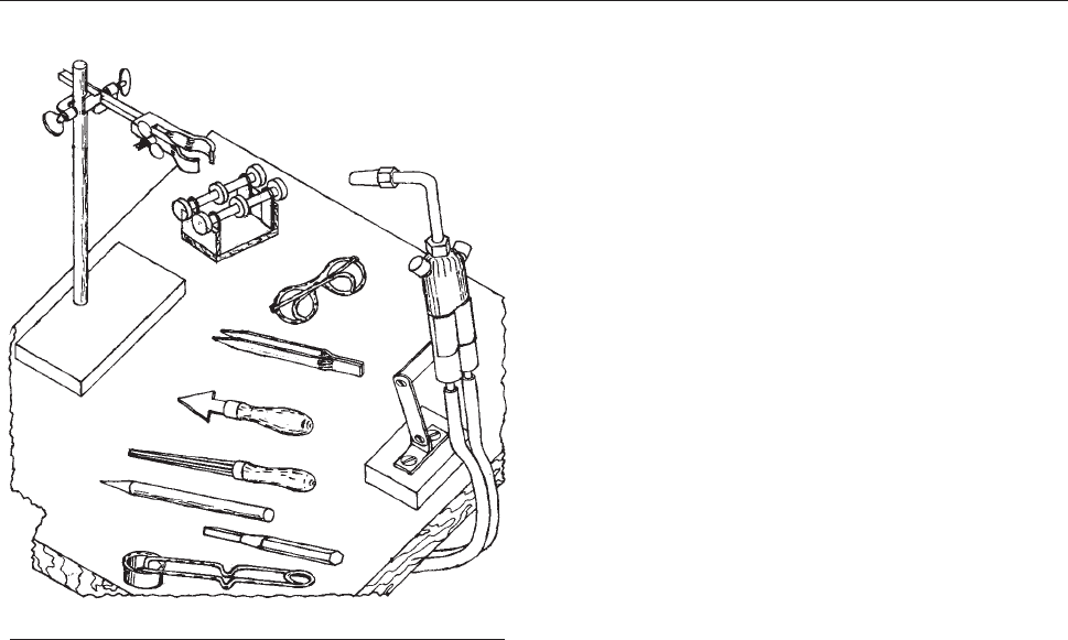
oxygen is required, along with two lengths of flexible
rubber or Tygon tubing for connecting the gas supplies
to the torch. A rigid ring stand and appropriate clamps
with fiberglass-covered jaws are needed to support glass
being worked upon. The torch and stand should be set up
on a fireproof bench top. Also required are a number of
small hand tools, inexpensively obtained from a scientific
supply house. These include a torch lighter, a wax pencil,
a glass-cutting knife, a swivel, a mouthpiece (an old
tobacco-pipe bit will do), glassblowing tweezers, a collec-
tion of corks and one-hole stoppers, and a variety of ream-
ing tools. These reaming tools consist of flat triangular
pieces of brass fitted with wooden file handles, and tapered
round or octagonal carbon rods in various sizes. Didymium
eyeglasses are necessary to filter out the intense sodium
D-line emission produced when glass is exposed to the
flame. Without these it is impossible to see hot glass as
it is worked. Clip-on didymium lenses are available for
these who wear prescription eyeglasses.
A little preliminary practice with the hand torch is
advisable. The gas inlet may be connected directly to a
low-pressure natural-gas outlet in the lab. The outlet valve
is turned completely open and gas flow is controlled by the
valve in the body of the torch. Oxygen is usually obtained
from a high-pressure cylinder. A pressure regulator for the
oxygen tank is essential. The outlet pressure should be
between 40 and 70 kN/m
2
(6 and 10 psi). Once again,
the flow of oxygen gas is controlled by the valve in the
body of the hand torch. The proper procedure is to open the
gas control and ignite the gas first. The gas should be
adjusted to give a flame 5 to 8 cm long before the oxygen
is introduced. If the flame blows out, the oxygen valve
should be closed and the gas permitted to flow for a few
moments to purge the torch of the explosive gas–oxygen
mixture before reignition is attempted.
With a #3 torch tip it is possible to produce a range of
flames suitable for work on tubing from a few millimeters
up to 50 mm in diameter. Opening the gas valve wide and
adding only a little oxygen gives a large, bushy yellow
flame. This is a cool reducing flame suitable for preheating
large pieces of glass and for annealing finished work. At
the opposite extreme, a sharp blue oxidizing flame can be
obtained by restricting the gas flow. For work on fine tub-
ing and for cutting tubing it is possible to make a flame no
more than 3 cm long and 3 mm in diameter. The hottest
flame is made with an excess of oxygen. The hottest part of
the flame is the tip of the blue inner cone.
Some practice will be required to master even the simple
operations described below. The neophyte should obtain
the necessary tools and a supply of clean dry borosilicate
glass tubing of 8–12 mm diameter. About ten hours of
practice is required before one can profitably embark on
any serious apparatus construction.
2.3.2 Cutting Glass Tubing
Tubing up to about 12 mm diameter can be broken cleanly
by hand. The location of the desired break may be indi-
cated by marking the tubing with a wax pencil. The glass is
then scored with a glass knife or the edge of a triangular
file, as shown in Figure 2.5. The scratch should be perpen-
dicular
to the axis of the tube and need only be a few
millimeters in length. Use considerable pressure and make
only one stroke. Do not saw at the glass. Wet the scratch
and then, holding the tubing as shown in Figure 2.6 with
the
scratch toward you, push the ends apart. Applying a
Figure 2.4 Glassblower’s equipment.
82 WORKING WITH GLASS
force that tends to bend the ends of the tube away from
you, while simultaneously pulling, will facilitate a clean
break.
Tubing of 12 to 25 mm diameter can be cut by cracking
it with a flame. First score the glass around approximately
one third of its circumference with the glass knife. Then
wet the scratch and touch the end of the scratch with a very
fine sharp flame that is oriented tangentially to the circum-
ference, as shown in Figure 2.7.
Lar
ge-diameter tubing can be parted by cracking it using
a resistively heated wire held in a yoke, as illustrated in
Figure 2.8. The tubing is placed on the resistance wire with
one
end butted against a stop. The wire is heated red-hot by
passing current through it, and the tube is rotated to heat a
narrow zone around its circumference. After a moment the
tube is quickly removed and the hot zone is brushed with a
wet pipe cleaner. The thermal shock thus produced should
result in a clean break.
The edge of the glass at a fresh break is sharp and
fragile. After cutting, the end of a tube can be fire-polished
to relieve this hazardous condition. This is accomplished
simply by heating the end of the tube in the flame until the
glass is soft enough that surface tension rounds and thick-
ens the sharp edge.
2.3.3 Pulling Points
Points are elongations on the end of a tube produced by
heating the glass and stretching it. These points serve as
Figure 2.6 Breaking glass tubing. The tubing is bent and
simultaneously pulled apart.
Figure 2.7 Cracking tubing with a flame.
Figure 2.5 Scoring glass tubing in preparation for break-
ing. Use only one stroke with considerable force.
Figure 2.8 Device for cutting large-diameter glass tubing.
LABORATORY GLASSBLOWING SKILLS 83
handles for manipulating short pieces of tubing. Pulling a
point is the first step in closing the end of a tube.
The procedure for pulling points depends upon whether
the tubing can be rotated or not. If the tubing is free, then
place the torch in its holder with the flame pointed away
from you and hold the glass in both hands as illustrated in
Figure 2.9. Adjust the torch to give a fairly full, neutral
flame.
Then, rotating the glass at a uniform rate, pass it
through the flame to heat a zone about as wide as the tube
diameter. When the glass softens, remove it from the flame
and pull the heated section to a length of about 20 cm.
Then quickly heat the center of the stretched section and
pull the glass in two, leaving a small bead at the end of
each point. It is important that the points be on the axis
of the original tube. This requires that the circumference of
the tube be heated uniformly and that the ends of the tube
be pulled straight away from one another. Some practice is
required to synchronize the motion of the hands so that
both ends of the tubing are rotated in such a way that the
tube does not twist or bend when it becomes pliable in the
flame. Beginners tend to overheat glass, thus exacerbating
this problem of misalignment. When glass is sufficiently
plastic for proper manipulation, it is still rigid enough to
help support the end sections.
If one end of a tube is attached, so that the tube cannot
be rotated, then it becomes necessary to swing the torch
around the tubing rather than rotate the glass before the
stationary torch. Some practice is required to achieve a
smooth motion with the torch so that the tube is heated
uniformly around its circumference. The unattached end of
the tubing is supported with the free hand until the glass is
sufficiently hot to be pulled.
2.3.4 Sealing Off a Tube: The Test-Tube End
Tubing is closed off by forming a hemispherical bubble
similar to that found at the end of a test tube. In order for
the test-tube end to form a strong closure, it must be
smooth and of a uniform thickness. The hemispherical
shape is formed by closing off the tubing and then soften-
ing the glass in the flame and blowing into the tube.
Begin by pulling a point on the tubing that is to be closed
off. If the tubing is not rigidly mounted, place it in a clamp
secured to a ring stand on the workbench. If possible the
work should be at chest height with the point upward. Press
a one-hole stopper, with a piece of soft rubber tubing
attached, into the open end of the tube as shown in Figure
2.10. Warm the glass at the base of the point with a soft
bush
y flame. Adjust the gas–oxygen mixture to the torch to
give a fairly small flame with a well-defined, blue inner
cone. Heat the point close to the shoulder where it joins the
tube. Swing the torch around the work so that the glass is
heated uniformly. When the glass melts, pull the point off
the tube. Only a small bead of glass should be left behind.
A large blob of glass will result in a closure that is too thick
in relation to the wall of the tubing. A test-tube end that is
thick in the middle and thin at the sides will develop
destructive strains, since it does not cool at a uniform rate.
The key is to heat only a narrow zone of the point near the
shoulder and to perform the whole operation rather
quickly. If a large globule of glass is left after pulling off
the point, the excess must be removed. With a sharp flame,
heat the globule until it melts. Remove the flame, touch the
molten bead with the end of a piece of glass rod (‘‘cane’’),
and quickly pull the rod away. Excess glass will be pulled
away from the soft bead into a fiber which can be broken or
melted off. The test-tube end is completed by heating the
closed-off end as far as the shoulder with a somewhat larger
flame until it is soft and the glass has flowed into a fairly
uniform thickness. The flame should be directed downward
at the end of the tube with a circular motion. Remove the
flame and gently blow the end into a hemispherical shape.
Figure 2.9 Pulling points.
84 WORKING WITH GLASS
If a flat end is desired, reheat the round end and gently
blow while pressing a flat carbon block against the end.
2.3.5 Making a T-Seal
A tube is joined at a right angle to the side of another tube
with a T-seal. To make a T-seal, close one end of a tube
with a cork and attach the blow tube to the other. If pos-
sible, mount the tube horizontally at chest height. With a
sharp flame heat a spot on the top side of the tube. Using a
circular motion of the torch, soften an area about the size
of the cross-section of the tube that is to be joined. Then
move the flame away and gently blow out a hemispherical
bulge, as shown in Figure 2.11(b). Reheat the bulge and
blo
w out a thin-walled bubble. Finally, while blowing to
pressurize the inside of the tube, touch the bubble with the
tip of the flame so that a hole is blown through it. Now heat
the edge of this hole so that surface tension pulls the glass
back to the edges of the original bubble. The result should
be a round opening slightly smaller than the diameter of
the tube that is to be joined, as shown in Figure 2.11(f).If
the
opening is too small or if the edge is irregular, the hole
can be reamed and shaped by softening the glass and shap-
ing the hole with a tapered carbon. A tool for this job can
be made by sharpening a 1/4 in. diameter carbon rod in a
pencil sharpener.
With a cork or a point, close off the end of the tube that
is to be sealed to the horizontal tube. Then, holding this
tube above the hole and tipped slightly back, simultane-
ously heat the edges of the tube and the hole until they
become soft and tacky. Bring the tube into contact with the
back edge of the hole, remove the flame, and tip the tube
forward until it rests squarely on the hole. The tacky edges
should join together to produce an airtight seal. Blow to
check the seal. Small holes can be closed by heating the
seal all around until the glass is soft, and tipping the ver-
tical tube in the direction of the leak. It also is possible to
‘‘stitch’’ a gap closed with cane. This is done by pulling a
Figure 2.10 Blowing a test-tube end.
LABORATORY GLASSBLOWING SKILLS 85
point on a piece of glass rod. Then warm the gap which is
to be repaired, heat the point of the cane until it is molten
and deposit the tiny blob of molten glass thus produced
into the gap. The seal at this point is quite fragile because
the glass is too thick around the seal. Cracks will develop if
the glass is permitted to cool before the seal is blown out in
order to reduce the wall thickness.
Glassblowing around the seal proceeds in four steps.
Begin with a sharp flame parallel to the axis of the horizon-
tal tube. Swing the torch back and forth to heat one quadrant
Figure 2.11 Steps in making a T-seal.
86 WORKING WITH GLASS
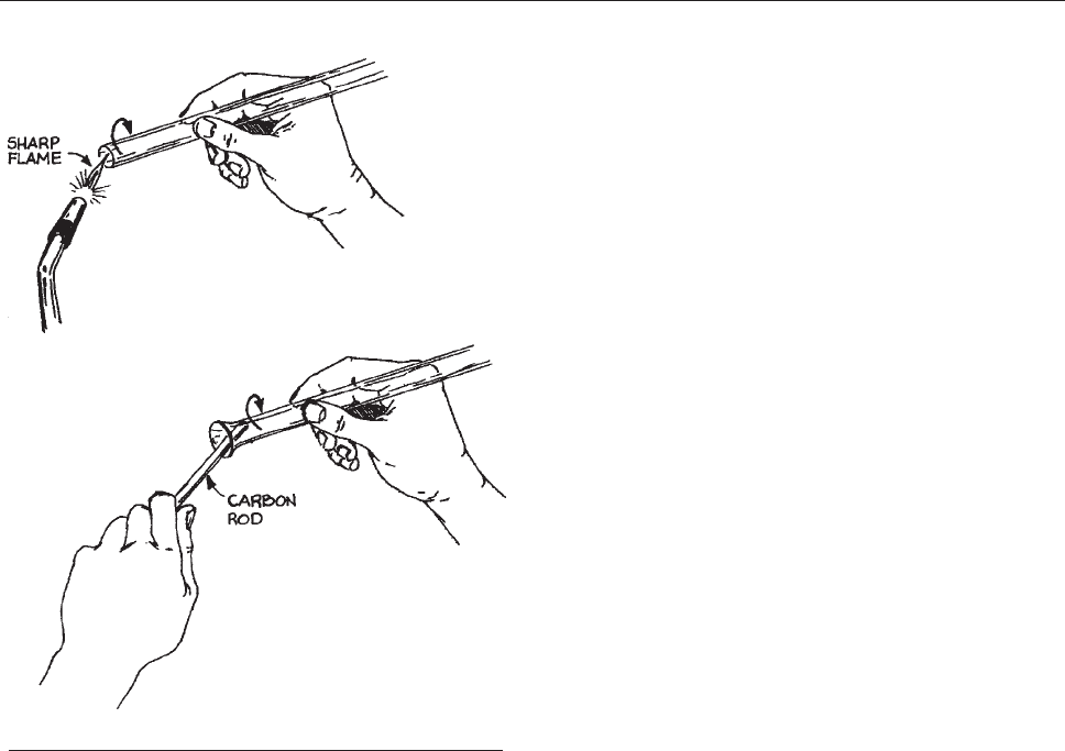
of the seal. When the glass softens, remove the flame and
blow gently. Timing is important here. Blowing while the
glass is in the flame will cause the thinnest parts to bulge. If,
however, one waits a moment after removing the flame, the
thinnest parts will cool and blowing will preferentially thin
out the thick portions of the seal, yielding a more uniform
wall thickness. The joint between the vertical and horizontal
tubes should then be a smooth curve of glass. During the
blowing operation the vertical tube must be held with the
free hand to prevent its tipping or sagging into the horizontal
tube. Next repeat the heating and blowing operation on the
side diametrically opposite. Finally, in a third and fourth
step, blow out the remaining two quadrants.
2.3.6 Making a Straight Seal
A straight seal joins two tubes coaxially. There are two
simple procedures for making such a seal.
If the tubes are quite different in diameter, close off the
larger one with a test-tube end and mount it vertically with
the closed end up. Then blow a bubble of the appropriate
size in the test-tube end and proceed as in making a T-seal.
Alternatively, the smaller tube can be flared out to the
diameter of the larger one. The flaring operation is illus-
trated in Figure 2.12. With the torch in its stand, heat the
edge
of the tube by rotating it in a sharp flame. Remove it
from the flame, and while continuing to rotate the tube,
insert a tapered carbon and gently bring the soft edge of the
glass up against the taper. Do not attempt to produce a flare
of the desired diameter in one rotation of the tube. It will
not come out round. The flaring operation is much easier if
the tube is placed on a set of glassblower’s rollers.
As shown in Figure 2.13(a), the larger tube should
be
mounted vertically if possible. Suspend the smaller tube
with the flare just above the larger one. With the upper tube
tipped back slightly, heat the edges of the larger tube and
the rim of the flare until the glass is tacky. Bring them into
contact at the back of the seal, remove the flame, and tip
the upper piece forward to join the two pieces. Proceed to
blow out the seal in four steps as for the T-seal. Minimize
the distance above and below the seal over which the glass
is heated.
2.3.7 Making a Ring Seal
A ring seal is used for sealing a tube inside a larger tube,
as in Figure 2.14(f), or for passing a tube through the wall
of
a container. There are many procedures for making
such se als. The s implest involves bulging the smaller-
diameter tube sufficiently for it to close off the hole
through which the tube must pass. A bulge in a tube is
known as a maria. Making a maria is a freehand oper-
ation and requires some practice.
Begin with the torch in its holder and the gas supply
adjusted to give a long, na rrow flame. Then rotating
the tubing in both hands, heat a very narrow zone at the
desired location. As soon as the glass softens, drop the
tube out of the flame, and, with your elbows braced on
the bench top or against your sides, push the e nds of the
tube toward one another. If the tube has been heated uni-
formly around and the ends are held coaxial, a bulge
should develop around the tube. If the heating is not uni-
form, the tube will bend. If the glass is too soft, the ends
Figure 2.12 Flaring the end of a tube.
LABORATORY GLASSBLOWING SKILLS 87
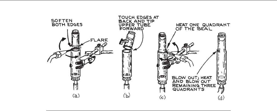
of the tube are liable to move out of alignment and an
eccentric bulge will result. When a uniform bulge is
attained, reheat it, remove it from the flame, and push
again to increase the dia met er of the ma ria. The bulge
should be solid glass. If too wide a zone is heated, the
maria will be hollow and dangerously fragile.
To make a coaxial ring seal between two tubes, form on
the smaller tube a maria of the same diameter as the larger.
Mount the larger tube vertically, fire-polish the top edge,
and rest the smaller tube on top, as in Figure 2.14(e). With
a
small flame, heat the junction uniformly between the
maria and the edge of the larger tube. The weight of the
smaller tube should cause it to settle and become fused to
the larger one. Finally blow out the seal in four steps, as in
making a conventional seal. Exercise care to prevent the
wall of the outer tube from sagging into the inner tube. If
the inner tube is not centered, it can be realigned by soft-
ening the seal with a cool, bushy flame and manipulating
its protruding end.
2.3.8 Bending Glass Tubing
Bends are best made beginning with the tubing vertical
[Figure 2.15(a)]. Close off the upper end with a cork or a
point
and attach the blowtube to the other end. While
supporting the upper end of the tube with the free hand,
apply a large bushy flame at the location of the desired
bend. Heat the glass uniformly over a length equal to about
four times the diameter of the tube. When the glass
becomes pliable, remove the flame and quickly bend the
upper end over to the desired angle. As soon as the bend is
completed, blow to remove any wrinkles which may have
developed and to restore the tubing to its original diameter.
Some reheating may be necessary.
A sharp right-angle bend can be produced by first mak-
ing a T and then pulling off one running end of the T close
to the seal [Figure 2.15(b)]. Blow out a test-tube end where
the
tubing is pulled off.
2.3.9 Annealing
Even when a seal is carefully blown out to give a uniform
wall thickness, harmful stresses are inevitably frozen into
the glass. Worked glass must be annealed by heating to a
temperature above the annealing point (see Table 2.1) and
then
slowly cooling to the strain point. In a large profes-
sional glass shop, special ovens are employed for this
operation. In the lab, however, glass must be annealed in
the flame of the torch. After a piece of glass has been
blown, it is heated uniformly over a wide area surrounding
the work with a large, slightly yellow, bushy flame. For
Pyrex 7740 the glass should be brought to an incipient
red heat. Care must be taken to prevent the glass from
becoming so hot that it begins to sag under its own weight.
The heated work is then cooled by slowly reducing the
oxygen to the torch until the flame becomes sooty.
Figure 2.13 Steps in making a straight seal.
88 WORKING WITH GLASS
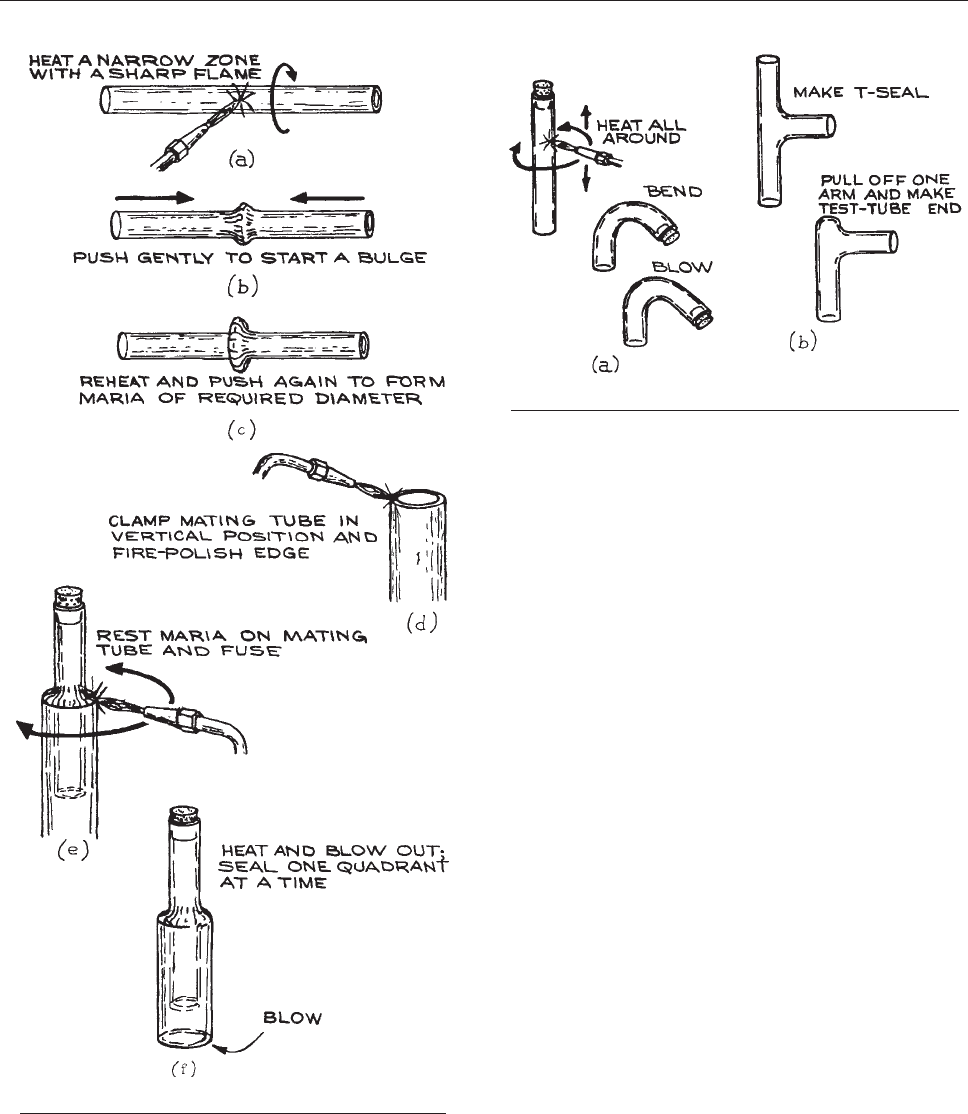
When soot begins to adhere to the glass, the flame can be
removed.
Areas in glass which are under stress will rotate the plane
of polarization of transmitted light. A polariscope can be
used to observe strain in glass in order to test the effective-
ness of the annealing operation. A polariscope can be pur-
chased from a laboratory supplier or can be constructed with
high-extinction sheet polarizers, as shown in Figure 2.16.
Th
e polarizers are crossed so that unstrained glass appears
dark when placed between them. Areas of strain rotate the
plane of polarization and appear bright, as in Figure 2.17.A
la
rge stationary piece of glasswork, such as a vacuum mani-
fold, can be tested by illuminating it from behind with ver-
tically polarized light and then viewing the work through
Polaroid sunglasses (which transmit horizontally polarized
light). A suitable source can be constructed by placing a
100 watt lamp behind a diffuser in a ventilated, open-top
box, and covering the box with a sheet of polarizer sand-
wiched between glass plates.
2.3.10 Sealing Glass to Metal
Glass-to-metal seals are fragile and difficult to produce in
the lab. The simplest means of attaching metal tubing
to a glass system or of passing a metallic electrode through
a glass wall is to make use of a commercially produced
glass-to-metal seal [Figure 3.28(b)]. If necessary a direct
Figure 2.14 Steps in making a ring seal.
Figure 2.15 Bending tubing.
LABORATORY GLASSBLOWING SKILLS 89
seal between a variety of metals and glasses can be pro-
duced with careful attention to design and fabrication.
2
Of
these, the tungsten-to-Pyrex seal is most easily and reliably
fabricated in the lab.
Although the linear coefficient of expa nsion of tung-
sten is about 50% greater than that of 7740 borosilicate
glass, it is possible to m ake a strong, vacuum-tight seal
between Pyrex and tungsten wire or rod of up to a milli-
meter diameter.
3
Since the glass will wet tungsten oxide,
but not tungsten, it is necessary that the metal surface be
properly prepared. Tungsten wire or rod usually has a
longitudinal grain by virtue of the method of manufac-
ture. The metal stock should be cut to length by grinding
to prevent splintering. To pr event gas from leaking
through the seal along the length of the wire it is good
practice to fuse the ends of the wire in an electric arc.
Alternatively, a copper or nickel wire can be welded to
each end of the tungsten wire. Tungsten electrodes with
co pper or nickel wires attached are also available from
commercial sources. Holding the wire in a pin vise, heat
the area to be sealed to a dull red and i mmediately rub the
hot metal with a stick of sodium nitrite. The salt com-
bines with the tungsten oxide to leave a clean metal sur-
face. Rinse the metal with tap water to remove the salt
and then rinse with distilled water. The metal must then
be reoxidized in an oxygen-rich flame to produce an
oxide layer of the proper thickness. If the layer is too
thick it will pull away from the metal; if it is too thin it
may all dissolve into t he glass. The clean tungsten should
be gently heated only until the metal appears blue-green
when cool. A piece of 7740 glass, 2 cm long with a wall
thickness of about 1 mm and an inner diameter slightly
larger than the tungsten wire, is slipped over the wire and
slid along to the sealing position. Be careful not to
scratch the oxide layer. T he glass tube is fused to the
metal using a small, sharp flame. Melting should proceed
from one end to the other with continuous rotation to
pr event trapping air. If t he metal is properly wett ed by
the glass, the wire will appear oversize where it passes
through the seal. A copper or amber color after the seal is
cool indicates a good seal. The beaded tungsten rod is
then sealed into the apparatus, as in making a ring seal
(Section 2.3.7). If necessary, a shoulder can be built up
around
the middle of the bead by fusing on a winding of
1 mm glass rod.
A tungsten-to-Pyrex seal makes an excellent electrical
feedthrough. Wires can be brazed or spot-welded to either
end of the tungsten rod. Since tungsten is not a good elec-
trical conductor, care must be taken to ensure that electri-
cal currents do not overheat the feedthrough. The safe
current-carrying capacity of the tungsten in this applica-
tion is about 8 Amm
2
.
Figure 2.16 A polariscope.
Figure 2.17 The appearance of strain in unannealed glass
as seen in the polariscope.
90 WORKING WITH GLASS
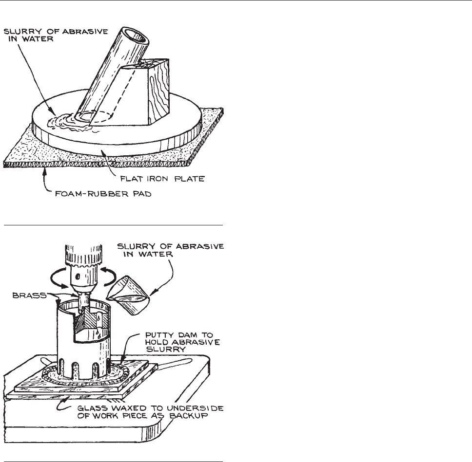
2.3.11 Grinding and Drilling Glass
In many instances the ends of a tube must be ground square
or at an angle, or a tube must be ground to a specific length.
The ends of a laser tube, for example, must be cut and
ground to Brewster’s angle before optical windows are
glued in place. Grinding a plane surface is performed in
a water slurry of abrasive on a smooth iron plate. It is done
with a circular motion while applying moderate pressure.
The work should be lifted from the surface frequently in
order to redistribute the abrasive. If the angle of the ground
surface relative to the workpiece is not critical, the work
can be grasped in the hand; otherwise, a wooden jig, such
as is shown in Figure 2.18, may be fabricated to orient the
work
with respect to the grinding surface.
Carborundum or silicon carbide grit of #30, 60, 120, and
220 mesh is used for coarse grinding, and emery of #220,
400, and 600 mesh is used for fine grinding. In any grind-
ing operation, begin with the grit required to remove the
largest irregularities and proceed in sequence through the
finer grits. Before changing from one grit to the next finer,
the work and the grinding surface must be scrupulously
washed so that coarse abrasive does not become mixed
with the next finer grade. Before changing from one grit
to the next, it is useful to inspect the ground surface under
a magnifying glass. If the abrasive in use has completed its
job, the scratch marks left by the abrasive should be of a
fairly uniform width.
Holes can be cut in glass, and round pieces of glass can be
cut from larger pieces, with a slotted brass tube drill – a
‘‘cookie cutter’’ – in a drill press (Figure 2.19). These drills
are
easily fabricated in sizes from several millimeters to
many centimeters in diameter. Either flat or curved glass
can be drilled. Cutting is accomplished by continuously feed-
ing the drill with a slurry of #60 or #120 mesh abrasiv e. It is
usually most convenient to form a dam of soft wax or putty
around the hole location to hold the slurry of abrasi ve around
the drill. Work slo wly with a light touch at a drill speed of
50–150 rpm. The tool should be backed out frequently to
permit the abrasive to flow under. Because grinding action
occurs along both the leading edge and the side of the drill
tube, the finished hole will be some what larger than the drill
body. Frequently the edges of the hole will chip where the
drill breaks through on the under side of the work. This can
be prevented when drilling flat glass by backing up the work-
piece with a second piece of glass waxed onto the underside.
Glass can be sawn as well as drilled. Many glass shops
use a powered, diamond-grit cutting wheel for precision
cutting. In the absence of such a machine, it is possible to
cut glass in much the same manner as it is drilled. A hack-
saw with a strip of 20-gauge copper as a blade is used. The
Figure 2.18 A wooden jig used in grinding the face of
a piece of tubing.
Figure 2.19 Drilling glass with a tube drill.
LABORATORY GLASSBLOWING SKILLS 91

work is clamped in a miter box and sawn with a light touch
while feeding an abrasive slurry to the blade.
Cited References
1. W. G. Housekeeper, Trans, A.I.E.E., 42, 870, 1923.
2. F. Rosebury, Handbook of Electron Tube and Vacuum Tech-
niques, Addison-Wesley, Reading, MA, 1965, pp. 54–66.
3. J. Strong, Procedures in Experimental Physics, Prentice-Hall,
Englewood Cliffs, NJ, 1938, p. 24; G. W. Green, The Design
and Construction of Small Vacuum Systems, Chapman and
Hall, London, 1968, pp. 100–102.
General References
W. E. Barr and J. V. Anhorn, Scientific and Industrial Glass
Blowing and Laboratory Techniques, Instruments Publishing,
Pittsburgh, 1959.
Corning Glass Works, Laboratory Glass Blowing with Corning’s
Glasses, Publ. No. B-72, Corning Glass Works, Corning, NY.
J. E. Hammesfahr and C. L. Strong, Creative Glass Blowing,
Freeman, San Francisco, 1968.
W. Morey, The Properties of Glass, Reinhold, New York, 1954.
F. Rosebury, Handbook of Electron Tube and Vacuum
Techniques, Addison-Wesley, Reading, MA, 1965.
92 WORKING WITH GLASS

VACUUM TECHNOLOGY
In the modern laboratory, there are many occasions when a
gas-filled container must be emptied. Evacuation may sim-
ply be the first step in creating a new gaseous environment.
In a distillation process, there may be a continuing require-
ment to remove gas as it evolves. Often it is necessary to
evacuate a container to prevent air from contaminating a
clean surface or interfering with a chemical reaction. Beams
of atomic particles must be handled in vacuo to prevent loss
of momentum through collisions with air molecules. Many
forms of radiation are absorbed by air and thus can prop-
agate over large distances only in a vacuum. A vacuum
system is an essential part of laboratory instruments such
as the mass spectrometer and the electron microscope. Far
infrared and far ultraviolet spectrometers are operated
within vacuum containers. Simple vacuum systems are used
for vacuum dehydration and freeze-drying. Nuclear particle
accelerators and thermonuclear devices require huge,
sophisticated vacuum systems. Many modern industrial
processes, most notably semiconductor device fabrication,
require carefully controlled vacuum environments.
3.1 GASES
The pressure and composition of residual gases in a vac-
uum system vary considerably with its design and history.
For some applications a residual gas density of tens of
billions of molecules per cubic centimeter is tolerable. In
other cases no more than a few hundred thousand mole-
cules per cubic centimeter constitutes an acceptable vac-
uum: ‘‘One man’s vacuum is another man’s sewer’’.
1
It is
necessary to understand the nature of a vacuum and of
vacuum apparatus to know what can and cannot be done,
to understand what is possible within economic con-
straints, and to choose components that are compatible
with one another as well as with one’s needs.
3.1.1 The Nature of the Residual Gases
in a Vacuum System
The pressure below one atmosphere is loosely divided into
vacuum categories. The pressure ranges and number
densities corresponding to these categories are listed in
Table 3.1. Vacuum science has been slow in adopting the
SI
unit of pressure – the Pascal or Pa – preferring instead
torr or bar. We will follow this preference. For the purposes
of the discussion here, a pressure of 1 torr, 1 millibar, and
100 Pa can be taken as equivalent. As a point of reference
for vacuum work, it is useful to remember that the number
density at 1 mtorr is about 3.5 3 10
13
cm
3
and that the
number density is proportional to the pressure.
The composition of gas in a vacuum system is modified
as the system is evacuated because the efficiency of a
vacuum pump is different for different gases. At low pres-
sures molecules desorbed from the walls make up the
residual gas. Initially, the bulk of the gas leaving the walls
is water vapor and carbon dioxide; at very low pressures, in
a container that has been baked, it is hydrogen.
3.1.2 Gas Kinetic Theory
In order to understand mass flow and heat flow in a vacuum
system it is necessary to appreciate the immense change in
93
CHAPTER
3
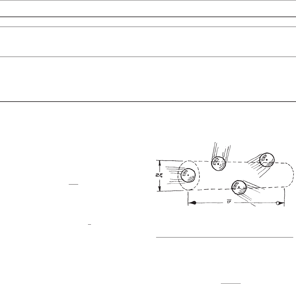
freedom of movement experienced by a gas molecule
as the pressure decreases.
The average velocity of a molecule can be deduced
from the Maxwell–Boltzmann velocity distribution law:
v ¼
8kT
pm
1=2
ð3:1Þ
For an air molecule (molecular weight of about 30 amu)
at 20 ºC:
v 5 3 10
4
cm s
1
¼
1
2
km s
1
ð3:2Þ
Each second a molecule sweeps out a volume with a diam-
eter twice that of the molecule and a length equal to the
distance traveled by the molecule in a second. As shown in
Figure 3.1, this molecule collides with any of its neighbors
whose center lies within the swept volume. The number of
collisions per second is equal to the number of neighbors
within the swept volume. On average, the number of col-
lisions per second (Z) is the number density of molecules
(n) times the volume swept by a molecule of velocity
v and
diameter n. More precisely:
Z ¼
ffiffiffi
2
p
npn
2
v ð3:3Þ
where the
ffiffiffi
2
p
accounts for the relative motion of the
molecules. The time between collisions is the reciprocal
of this collision frequency, and the average distance
between collisions, or mean free path, is:
k ¼
mZ
1
¼
1
ffiffiffi
2
p
npn
2
ð3:4Þ
Note that the mean free path is independent of the temper-
ature and the molecular weight.
The mean free path is inversely proportional to the pres-
sure. For an N
2
or O
2
molecule, n 3 3 10
8
cm. The
number density at 1 mtorr is about 3.5 3 10
13
cm
3
. Thus
the mean free path in air at 1 mtorr is about 5 cm. Recalling
Figure 3.1 The volume swept in one second by a
molecule of diameter n and velocity
v (cm/s). The molecule
will collide with any of its neighbors whose center lies within
the swept volume.
Table 3.1 Air at 20 ºC
Pressure
(torr)
a
Number Density
(cm
3
)
Mean Free
Path
(cm)
Surface Collision
Frequency
(cm
2
s
1
)
Time for
Monolayer
Formation
b
(s)
One atmosphere 760 2.7 3 10
19
7 3 10
6
3 3 10
23
3.3 3 10
9
Lower limit of:
Rough Vacuum 10
3
3.5 3 10
13
543 10
17
2.5 3 10
3
High Vacuum 10
6
3.5 3 10
10
5 3 10
3
4 3 10
14
2.5
Very High Vacuum 10
9
3.5 3 10
7
5 3 10
6
4 3 10
11
2.5 3 10
3
7Ultrahigh Vacuum 10
12
3.5 3 10
4
5 3 10
9
4 3 10
8
2.5 3 10
6
a
1 torr ¼1.33 mbarr ¼133 Pa
b
assumes unit sticking coefficient and a molecular diameter of 3 3 10
8
cm
94 VACUUM TECHNOLOGY

the relationship between k and P, a valuable rule of thumb
is that for air at 20 ºC:
k
5
PðmtorrÞ
cm ð3:5Þ
3.1.3 Surface Collisions
The frequency of collisions of gas molecules with a sur-
face is:
Z
surface
¼
nv
4
ðs
1
cm
2
Þð3:6Þ
The sticking probability for most air molecules on a clean
surface at room temperature is between 0.1 and 1.0. For
water the sticking probability is about unity for most surfa-
ces. Assuming unit sticking probability and a molecular
diameter n 3 3 10
8
cm, the time required to form a
monolayer of adsorbed air molecules at 20 ºCis:
t ¼
2:5 3 10
6
PðtorrÞ
s ð3:6Þ
Thus to maintain a clean surface for a useful period of
time may require a gas pressure over the surface less than
10
9
torr.
3.1.4 Bulk Behavior versus
Molecular Behavior
The pressure of gas within a vacuum system may vary over
10 or more orders of magnitude as the system is evacuated
from atmospheric pressure to the lowest attainable pres-
sure. At high pressures, when the mean free path is much
smaller than the dimensions of the vacuum container, gas
behavior is dominated by intermolecular interactions.
These interactions, resulting in viscous forces, ensure good
communication among all regions of the gas. At high pres-
sures, a gas behaves as a homogeneous fluid. When the gas
density is decreased to the extent that the mean free path is
much larger than the container, molecules rattle around
like the balls on a billiard table (not a pool table, where
the ball density can be high), and gas behavior is deter-
mined by the random motion of the molecules as they
bounce from wall to wall. Gas flow in the high-pressure
regime is characterized as viscous flow and in the low-
pressure regime as molecular flow. In the typical laboratory
vacuum system the transition between the two flow
regimes occurs at pressures in the vicinity of 100 mtorr.
In the viscous-flow region where the mean free path is
relatively small, gas flow improves with increasing pres-
sure because gas molecules tend to queue up and push on
their neighbors in front of them. Gas flow is impeded by
turbulence and by viscous drag at the walls of the pipe that
is conducting the gas. In the viscous region the coefficients
of viscosity and thermal conductivity are independent of
pressure.
In the molecular-flow region, momentum transfer
occurs between molecules and the wall of a container,
but molecules seldom encounter one another. In the molec-
ular flow regime, a gas is not characterized by a viscosity.
Gas flows from a region of high pressure to one of low
pressure simply because the number of molecules leaving
a unit of volume is proportional to the number of mole-
cules within that volume. Gas flow is a statistical process.
At very low pressure a molecule does not linger at a sur-
face for a sufficient time to reach thermal equilibrium.
Thus thermal conductivity at low pressures is a function
of gas density, and the coefficient of thermal conductivity
depends upon the pressure and upon the condition of the
surface.
3.2 GAS FLOW
3.2.1 Parameters for Specifying Gas Flow
Before discussing vacuum apparatus it is necessary to
define the parameters used by vacuum engineers to char-
acterize gas flow.
The volume rate of flow through an aperture or across
the cross section of a tube is defined as the pumping speed
at that point:
S [
dV
dt
½Ls
1
;m
3
s
1
;ft
3
min
1
ðcfmÞ ð3:7Þ
The capacity of a vacuum pump is specified by the speed
measured at its inlet:
S
p
[
dV
dt
ðat pump inletÞð3:8Þ
GAS FLOW 95
The mass rate of flow through a vacuum system is
proportional to the throughput:
Q [ PS ½ðtorr L s
1
;Pam
3
s
1
; std cm
3
s
1
ða standard cubic centimeter
or std cm
3
or scc is 1 cm
3
at
273 K and 1 atm or 1:01 barÞ
ð3:9Þ
To determine the throughput it is necessary that the
pressure and speed be measured at the same place, since
these quantities vary throughout the system.
The ability of a tube to transmit gas is characterized by
its conductance C. The definition of conductance is anal-
ogous to Ohm’s law for electrical circuitry. The throughput
of a tube depends upon the conductance of the tube and the
driving force, which in this case is the pressure drop across
the tube:
Q ¼ P
1
P
2
ðÞC ðP
1
> P
2
Þð3:10Þ
Notice that conductance has the same units as pumping
speed.
3.2.2 Network Equations
A complicated network of tubes can be reduced to a single
equivalent conductance for the purpose of analysis. In
analogy to electrical theory once again, a number of tubes
in series can be replaced by a single equivalent tube with
conductance C
series
given by:
C
series
¼
1
C
1
þ
1
C
2
þ
1
C
3
...
1
ð3:11Þ
A parallel network can be replaced by an equivalent
conductor with conductance:
C
parallel
¼ C
1
þ C
2
þ C
3
þ ð3:12Þ
3.2.3 The Master Equation
By use of the network equations given above, an entire
vacuum system can be reduced to a single equivalent con-
ductance leading from a gas source to a pump, as shown in
Figure 3.2. The net speed of the system is:
S ¼
Q
P
1
ð3:13Þ
and the speed at the pump inlet is:
S
p
¼
Q
P
2
ð3:14Þ
Notice that the throughput is the same at every point
in this system, since there is only one gas source. The
throughput of the conductance is:
Q ¼ðP
1
P
2
ÞC ð3:15Þ
Upon substitution for P
1
and P
2
from the previous two
equations, this equation, after some rearrangement,
becomes:
1
S
¼
1
S
p
þ
1
C
ð3:16Þ
This is the master equation that relates the net speed of a
system to the capacity of the pump and the conductors
leading to the pump. From this equation we see that both
the conductance of a system and the speed of the pump
exceed the net speed of the system. In vacuum-system
design, economics should be considered. The cost of a
vacuum pump is usually greater than the cost of construct-
ing a tube leading from a vacuum container to the pump. In
order to achieve a given net speed for a system, it is most
economical to design a system whose equivalent conduc-
tance exceeds the required net speed by a factor of three or
four so that the speed of the pump need only exceed the net
speed by a small amount.
Figure 3.2 Analytical representation of a vacuum system.
96 VACUUM TECHNOLOGY

3.2.4 Conductance Formulae
In the viscous-flow region the conductance of a tube
depends upon the gas pressure and viscosity.
2
For a tube
of circular cross-section and in the absence of turbulence,
the conductance from the Hagen – Poiseuille derivation is:
C ¼ 32 600
D
4
gL
P
av
Ls
1
ð3:17Þ
when the diameter D and length L of the tube are in cen-
timeters, the average pressure P
av
is in torr, and the vis-
cosity of the gas, g, is in micropoise (lP). For air at 20 ºC
the conductance is:
C ¼ 180
D
4
L
P
av
Ls
1
ð3:18Þ
These equations are used for determining the dimen-
sions required for the lines connecting to a pump that
operates in the rough vacuum region. A complex system
is treated as a series of simple cylindrical tubes; the con-
ductance of each tube is calculated from the equation
above and the conductance of the whole system is deter-
mined using the network equations. Joints and elbows
between simple tubes will reduce the conductance of the
system so it is wise to specify tube diameters somewhat
oversize to offset conductance losses in the transitions
between simple cylindrical shapes.
In the molecular-flow region, conductance is independ-
ent of pressure. The conductance of a tube of circular
cross-section is:
C ¼ 2:6310
4
v
D
3
L
Ls
1
ð3:19Þ
when the diameter and length are measured in centimeters
and the average molecular velocity
v is in cm/s. For air at
20 ºC the conductance is:
C ¼ 12
D
3
L
Ls
1
ð3:20Þ
These equations are useful in determining the dimen-
sions of a high-vacuum chamber and the size of the tubes
leading to and from the chamber. As an example of poor
design consider the case of a vacuum chamber connected
to a 100 L/s diffusion pump by a tube 2.5 cm in diameter
and 10 cm long. The net speed of the pump and connecting
tube is:
S ¼
1
100
þ
1
19
1
¼ 16 L s
1
ð3:21Þ
The connecting tube is strangling the pump. Consider also
the pressure drop across the tube. Since the throughput is a
constant, one can write:
SP
1
¼ S
p
P
2
¼ Q ð3:22Þ
thus:
P
1
P
2
¼
S
p
S
¼ 6 ð3:23Þ
This result indicates the importance of proper location
of a pressure gauge. In this case a gauge at the mouth of the
pump would indicate a pressure six times lower than the
pressure in the vacuum container.
There are frequently occasions when a vacuum system
is divided into compartments at very different pressures
separated by a wall with an aperture whose diameter
exceeds its length (a so-called ‘‘thin aperture’’). In the
viscous-flow regime, the conductance of an aperture at
20 ºC is approximately:
C 20 A Ls
1
ð3:24Þ
where A is the area in cm
2
. In the molecular-flow region,
the conductance of an aperture for a gas of molecular
weight M is:
C ¼ 3:7
T
M
1=2
A Ls
1
ð3:25Þ
where A is the area in cm
2
. These equations are useful for
determining the rate of gas flow into a vacuum chamber
through an aperture in a gas-filled collision chamber or ion
source.
There is a transition region between the viscous- and
molecular-flow regions where the mean free path approx-
imately matches the dimensions of the container. For
laboratory-scale apparatus, the transition region falls in
the range of 500 mtorr down to 5 mtorr. A mathematical
description of this region is difficult. Fortunately one finds in
most vacuum systems that the transition region is encoun-
tered only briefly during pumpdown from atmosphere to
GAS FLOW 97

high vacuum. Conductance formulae, such as given above,
for flow in the viscous (high-pressure) region compared
to conductance formulae in the molecular (low-pressure)
region show two important differences: gas flow in the
viscous region depends upon the gas pressure and the
square of the cross-section of the conductor (i.e., D
4
),
whereas gas flow in the molecular flow region is independ-
ent of pressure and goes as the 3/2 power of the cross-
section. It follows that the formulae for conductance in
the molecular-flow region will give a conservative estimate
of the conductance in the transition region.
3.2.5 Pumpdown Time
The time required to pump a chamber of volume V from
pressure P
0
to P is:
t ¼
V
S
ln
P
0
P
ð3:26Þ
assuming a constant net pumping speed and considering
only the gas that resided in the container at the outset. A
typical high-vacuum system is rough-pumped to about 50
mtorr with a mechanical pump and then pumped to very
low pressures with a diffusion pump or some other pump
that works effectively in the molecular-flow region. The
pumpdown calculation is performed in two steps corre-
sponding to these two operations. In the low-pressure
regime, gas desorbing from the container walls may con-
tribute to the gas load and the rate of desorption will need
to be considered in estimating the pumpdown time.
3.2.6 Outgassing
The rate at which the pressure falls in a chamber at pres-
sures below about 10
5
torr is largely determined by the
rate of evolution of gas from the walls of the chamber
rather than by the speed of the pump. The rate of gas
evolution – outgassing – from solid materials depends both
on the nature of the solid and the adsorbate. Water and
carbon dioxide from the air are adsorbed most tenaciously.
A rough, porous, or polar surface adsorbs more gas than a
clean polished surface. The outgassing rate from a surface
decreases slowly, roughly as e
at
(a a property of the sur-
face and the adsorbate, as well as a strong function of
temperature). Baking a vacuum chamber to 150 to
200 ºC under vacuum will encourage outgassing and result
in a lower ultimate pressure after the chamber cools.
Following exposure to air, stainless steel outgases at
roughly 10
8
torr L s
1
cm
2
of surface area after an hour
of pumping at room temperature. A day of pumping may
be required to reduce this rate below 10
9
torr L s
1
cm
2
.
The outgassing rate from aluminum is more than 10 times
greater than for stainless steel. Outgassing from plastics is
roughly 10 times worse than from aluminum, and outgas-
sing from elastomers (rubber) is 10 times worse yet. Plas-
tics and rubbers have no use in a vacuum system that is to
achieve pressures below about 10
7
torr.
Consider, for example, the problem of maintaining a
base pressure of 10
7
torr in a stainless-steel chamber. If
the outgassing rate is 10
9
torr L s
1
cm
2
, a pumping
speed of 10
2
Ls
1
is required for every cm
2
of surface.
For a container 1 m in diameter and 1 m high, a pumping
speed of 400 L s
1
is needed. This speed is typical of a
high vacuum pump (a diffusion pump or turbomolecular
pump) with a nominal 4 in. (10 cm) diameter inlet port.
Without baking to further reduce the outgassing rate, a
pump 10 times larger (and nearly 10 times as expensive)
would be required to reduce the pressure to 10
8
torr;
ultrahigh vacuum is out of the question.
3.3 PRESSURE AND FLOW
MEASUREMENT
The pressure within a vacuum system may vary over more
than 13 orders of magnitude. No one gauge will operate
over this range, so most systems are equipped with several
different gauges.
The pressure ranges in which the various gauges are
useful are shown in Figure 3.7.
3.3.1 Mechanical Gauges
Hydrostatic Gauges. The simplest pressure gauges
are hydrostatic gauges such as the oil or mercury
manometer. A closed-end U-tube manometer filled with
mercury is useful down to 1 torr. Diffusion-pump oils,
such as Octoil, di-n-butyl phthalate, or Dow Corning
DC704 or DC705 silicone oils, may also be used as
98 VACUUM TECHNOLOGY
manometer fluids. Because the density of these oils is much
less than that of mercury, oil-filled manometers are useful
down to about 0.1 torr. As shown in Figure 3.3,anoil
manometer
should be made of glass tubing of at least 1 cm
diameter in order to reduce the effects of capillary
depression. To prevent oil adhesion to the walls, the
manometer should be cleaned with dilute hydrofluoric acid
before filling. A heater is usually provided to drive dissolved
gas from the oil prior to use.
3
A number of manometers hav e
been designed to increase the surface area of oil exposed to
the vacuum in order to hasten outgassing.
4
Both oil and
mercury manometers will contaminate a vacuum system
with vapor of the working fluid. If this is a problem, a cold
trap is placed between the gauge and the system to condense
the offending vapor. Mercury in a manometer can be isolated
and protected from chemical attack by floating a few drops
of silicone oil on top of the mercury column.
The McLeod gauge shown in Figure 3.4 is a complex
hy
drostatic gauge and is sensitive to much lower pressures
than a simple U-tube manometer. In the McLeod gauge, a
sample of gas is trapped and compressed by a known amount
(typically 1000:1) by displacing the gas with mercury from
the original volume into a much smaller volume. The pres-
sure of the compressed gas is measured with a mercury
manometer and the original pressure determined from the
general gas law. Of course, it is not possible to use a McLeod
gauge to measure the pressure of a gas that condenses upon
compression. With care, a high-quality McLeod gauge will
provide accuracy of a few percent do wn to about 10
4
torr.
Some gauges can be used at even lower pressures, but it is
necessary to consider the error caused by the pumping action
of mercury vapor streaming out of the gauge.
5
The McLeod gauge is constructed of glass and is easily
broken. If the mercury is raised into the gas bulb too
quickly, it can acquire sufficient momentum to shatter
Figure 3.4 McLeod gauge.
Figure 3.3 Oil manometer. The trap is intended to contain
the oil charge in the event that the low-pressure arm of the
manometer is accidentally open to the atmosphere.
PRESSURE AND FLOW MEASUREMENT 99

the glass. When a gauge is broken, the external air pressure
frequently drives a quantity of mercury into the vacuum
system. For this reason it is wise to place a ballast bulb of
sufficient volume to contain the mercury charge of the
gauge between the gauge and the system.
Mechanical Gauges. A number of different gauges
depend upon the flexure of a metal tube or diaphragm as
a measure of pressure. In the Bourdon gauge, a thin-wall,
curved tube, closed at one end, is attached to the vacuum
system. Pressure changes cause a change in curvature of
the tube. A mechanical linkage to the tube drives a needle
to give a pressure reading on a curved scale. Another type
of mechanical gauge contains a chamber divided in two by
a thin metal diaphragm. The volume on one side of the
diaphragm is sealed, while the volume on the other side is
attached to the system. A variation in pressure on one side
relative to the other causes the diaphragm to flex, and this
movement is sensed by a system of gears and levers that
drives a needle on the face of the gauge. The precision of
these gauges is limited by hysteresis caused by friction in
the linkage. To overcome this friction it is helpful to gently
tap the gauge before making a reading. Unlike the liquid
manometer, mechanical gauges are not absolute gauges.
The pressure scale and zero location on these gauges
must be calibrated against a McLeod gauge or U-tube
manometer. Mechanical gauges are useful down to 1 torr
with an accuracy of about 0.5 torr. They offer the
advantage of being insensitive to the chemical or
physical nature of the gas.
Piezoelectric Pressure Transducers. A piezo
transducer is an absolute, direct-reading device that
senses the gas pressure on a piezoelectric crystal. They
function in the 10
1
to 1000 torr range. Typical gauges
include the transducer and the sensor electronics in a
single compact unit (for example, MKS Instruments).
They are useful for monitoring roughing and foreline
pressures, and for inclusion in an interlock system to
control vacuum system operation (see Sections 3.6.1,
6.6.9, 6.6.10).
Capacitance Manometers. A capacitance manometer
is a diaphragm manometer wherein the position of the
diaphragm is determined from a measurement of
electrical capacitance. The gauge head is divided into
two chambers by a thin metal diaphragm that serves as
one plate of a capacitor; the second plate of the capacitor
is fixed in one of the chambers. A change in the pressure
difference between the two chambers results in a change in
capacitance as the flexible diaphragm moves relative to the
fixed plate. A sensitive capacitance bridge measures the
capacitance between the two plates and the capacitance is
converted to a reading of the pressure difference.
Capacitance manometers are inherently differential
pressure gauges; most, however, are manufactured to
read absolute pressure by sealing and evacuating one of
the chambers. This arrangement does not provide a truly
absolute gauge since the readout must be set to zero by
connecting the open chamber to a true zero pressure (i.e.,
several orders of magnitude less than the full-scale
reading). A capacitance manometer is designed so that
the flexible diaphragm touches the opposing capacitor
plate at a small overpressure. This protects the fragile
diaphragm from a sudden inrush of gas. As might be
expected, the capacitance measurement is very sensitive
to the temperature of the flexible diaphragm. High
precision gauge heads incorporate a heater and
temperature control that maintains the gauge head at a
constant temperature.
Capacitance manometers are available to measure pres-
sures from 1000 torr down to less than 10
4
torr. A single
gauge head is useful over a range of three to four orders of
magnitude with an accuracy of 0.01% full scale at the low
end of the pressure range and 0.5% or better at the high end
(e.g., a 1 torr gauge head reads 1 3 10
4
61 3 10
4
torr at
the low end and 1.0060.005 torr at the high end). Gauges
are calibrated by the manufacturer and have a reputation
for holding their calibration for years given careful use.
The electronics have a response time of about 10 ms. This
makes the capacitance manometer especially useful for
pressure control in a feedback loop.
3.3.2 Thermal-Conductivity Gauges
The thermal conductivity of a gas decreases from some
constant value above about 10 torr to essentially zero at
about 10
3
torr. This change in thermal conductivity is
used as an indication of pressure in the Pirani gauge and
the thermocouple gauge. In both gauges a wire filament is
100 VACUUM TECHNOLOGY
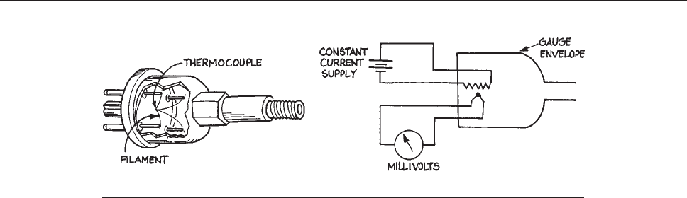
heated by the passage of an electrical current. The temper-
ature of the filament depends on the rate of heat loss to the
surrounding gas. In the thermocouple gauge, the pressure
is determined from the e.m.f. (electromotive force) pro-
duced by a thermocouple in contact with the filament
heated by the passage of a constant current (Figure 3.5).
In
the Pirani gauge, the heated filament is one arm of a
Wheatstone bridge. A change in temperature of the fila-
ment produces a change of resistivity and hence a change
in the voltage across the filament. The resulting imbalance
of the bridge gives an indication of pressure. Alternatively,
a voltage can be applied to keep the bridge in balance and
this voltage becomes the indication of pressure.
The pressure indicated by a thermocouple gauge or a
Pirani gauge depends upon the thermal conductivity of the
gas. They are usually calibrated by the manufacturer for
use with air. For other gases these gauges must be recali-
brated point-by-point over their entire range, since thermal
conductivity is a nonlinear function of pressure. In routine
use, a thermal-conductivity gauge can only be expected to
be accurate to within a factor of two. This accuracy is
adequate when the gauge is used to sense the foreline
pressure of a diffusion pump or to determine whether the
pressure in a system is sufficiently low to begin diffusion-
pumping. The principal advantages of these gauges are
their ease of use, ruggedness, and low cost.
3.3.3 Viscous-Drag Gauges
Above about 1 torr, the viscosity of a gas is constant, but, in
the molecular-flow regime, the viscous drag exerted by a
gas on a moving surface depends upon the gas density and
the mean velocity of the gas. It follows that below about
1 torr, a first-principles calculation yields gas pressure from
a measurement of viscous drag for a gas of known temper-
ature and composition. This approach to absolute pressure
measurement is applied in the spinning-rotor gauges man-
ufactured by Leybold AG and MKS Instruments.
In the gauge head of a spinning-rotor gauge, a magneti-
cally suspended steel ball is spun up to a rotational speed
of about 415 Hz by a rotating magnetic field. The drive is
interrupted and the ball is permitted to decelerate to a
preset lower speed, typically about 405 Hz. The pressure
is determined from a measurement of the time required for
a complete revolution of the coasting ball. The rate of
deceleration is very small – at 10
4
torr the deceleration
from 415 to 405 Hz takes many minutes. The measurement
of the ball rotation rate is repeated many times to obtain
satisfactory precision. A microprocessor in the controller
computes the statistical average of the deceleration rate
after many cycles.
Spinning-rotor gauges provide absolute pressure meas-
urement between 10
1
and 10
6
torr with an accuracy of a
few percent. At the lower end of this range, they are the
only available means for making highly accurate, repeat-
able, absolute-pressure measurements. Spinning-rotor
gauges are used as a transfer standard in calibrating other
types of gauges. These instruments must be maintained
with great care. They are expensive.
3.3.4 Ionization Gauges
In the region of molecular flow, pressure is usually meas-
ured with an ionization gauge or ‘‘ion gauge.’’ In this type
of gauge, gas molecules are ionized by electron impact and
the resulting positive ions are collected at a negatively
biased electrode. The current to this electrode is a function
Figure 3.5 Thermocouple gauge.
PRESSURE AND FLOW MEASUREMENT 101
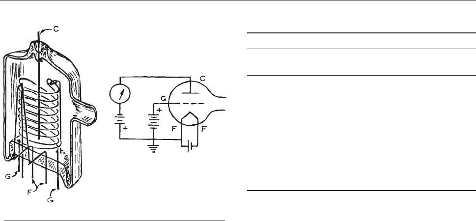
of pressure. There are two basic types of ion gauges, differ-
ing primarily in the mechanism of electron production. In
the hot cathode ionization gauge, electrons are produced
by thermionic emission from an electrically heated wire
filament. In cold cathode gauges, electrons and ions are
produced in a discharge initiated by a high-voltage elec-
trical discharge.
The most familiar configuration of the hot cathode ion-
ization gauge is that devised by Bayard and Alpert and
illustrated in Figure 3.6. The gauge electrodes are mounted
in
a glass envelope with a side arm that is attached to the
vacuum system. Electrons from an electrically heated fil-
ament (F) are accelerated through the gas toward a posi-
tively biased, helical wire grid (G). Collisions between the
accelerated electrons and gas molecules create ions that
are collected at a central wire electrode (C), and the pos-
itive ion current is measured by a sensitive electrometer.
These gauges are useful in the 10
3
to 10
10
torr range.
The ion current measured with an ionization gauge is a
linear function of pressure; the proportionality between
ion current depends upon the electron emission current
from the filament and upon the ionization efficiency of
the gas in the gauge. Commercial gauge controllers are
calibrated for use with air at a specified emission current,
typically about 10 mA. An adjustment on the controller
permits the user to set the emission current. For gases other
than air, the indicated pressure is multiplied by a sensitiv-
ity factor that is inversely proportional to the electron-
impact-ionization cross-section for the gas in question.
Sensitivity factors for some common gases are given in
Table 3.2.
Ion
gauges have the sometimes useful and sometimes
detrimental property of functioning as pumps. There are
two mechanisms for pumping. Ionized gas molecules
accelerated to and embedded in the collector are effec-
tively removed from the system. In addition, metal evapo-
rated from the filament deposits on the glass envelope of
the gauge to produce a clean, chemically active surface
that adsorbs nitrogen, oxygen, and water. At pressures
below 10
7
torr this pumping action may create a signifi-
cant pressure gradient between the gauge tube and the
system to which it is attached, resulting in a pressure read-
ing that is lower than that in the system. For ultrahigh-
vacuum systems the pumping problem is circumvented
by the use of ‘‘nude’’ gauges that consist of the gauge
electrodes mounted to a flange that is installed so that
the electrodes protrude into the system proper; there is
no envelope or tubulation joining the gauge to the system.
The pressure indicated by an ionization gauge is also
affected by the emission of gas adsorbed on the gauge
electrodes and envelope. To overcome this problem the
gauge is periodically degassed by heating the electrodes
Figure 3.6 Bayard–Alpert ionization gauge.
Table 3.2 Sensitivity factors for ionization gauges
Gas Formula Multiplicative
Factor
a
Air 1.0
Nitrogen N
2
1.0
Oxygen O
2
0.9
Hydrogen H
2
2.4
Carbon dioxide CO
2
0.7
Methane CH
4
0.7
Hydrocarbons C
4
and up 0.2
Argon Ar 0.9
Neon Ne 3.5
Helium He 6.8
a
Calibrated for air. Recommended values based primarily upon
the survey published by R. L. Summers, NASA Tech. Note: TN
D-5285, and an assumed nominal acceleration potential of 150V.
102 VACUUM TECHNOLOGY

and the envelope. This is accomplished by the gauge con-
troller in the ‘‘degas’’ mode in which an AC current is passed
through the grid to heat it to incandescence. Radiative
heating of the surrounding components encourages outgas-
sing. A hot cathode ionization gauge is activated when the
pressure falls below 10
3
torr – turn-on at higher temper-
atures will cause the filament to burn out. The gauge should
be degassed for a few minutes when the pressure falls to
about 10
4
torr and the degassing should be repeated with
each decrease of two orders of magnitude in pressure.
The electron-emissive filament in the ion gauge is made
of tungsten or thoria-coated iridium. Tungsten filaments
operate at 1800 ºC. They provide the most stable operation,
however, their lifetime is significantly shortened by expo-
sure to hydrocarbons at relatively high pressures. Thoria-
coated filaments operate at about 1200 ºC and can be
expected to be longer-lived than tungsten filaments. Many
gauge tubes provide two filaments with separate external
connections. Only one filament is activated at a time. When
the first filament burns out the second can be used so that
it is not necessary to let the system up to air pressure
following the first failure. When the filaments have failed
in a glass-enclosed gauge, the entire gauge is replaced.
Individual filaments are replaceable in nude gauges.
Cold cathode ionization gauges in various configura-
tions are identified as Penning gauges, magnetrons,
inverted magnetrons, and Philips gauges. In these gauges
an electrical discharge is struck in a low-pressure gas
between two electrodes maintained at a potential differ-
ence of several kV. The range of stability of the discharge
is extended by a magnetic field provided by a permanent
magnet that is an integral part of the gauge head. The
magnetic field confines the electrons in the discharge so
as to increase their pathlength through the gas. The dis-
charge current measured at one of the electrodes provides a
measure of the gas pressure. The measured current is rel-
atively much larger than that obtained with a hot-cathode
gauge – of the order of 1 A torr – thus greatly simplifying
the controller electronics. Cold cathode gauges operate in
the 10
2
to 10
7
torr range with an accuracy of a factor of
two at best. The pressure range is extended down to less
than 10
9
torr in some more complex designs. Without the
fragile filament of the hot cathode gauge, cold cathode
gauges are robust and economical, suffering primarily only
from their limited range of applicability.
The operating pressure ranges of the vacuum gauges is
shown in Figure 3.7.
3.3.5 Mass Spectrometers
A mass spectrometer can be used to determine the partial
pressures of residual gases in a system and to detect
leaks. Small, relatively inexpensive mass spectrometers
designed specifically for these purposes are called resid-
ual-gas analyzers (RGAs). These instruments employ quad-
rupole or magnetic-deflection type analyzers and typically
cover the mass range from 2 to 100 amu. They are sensitive
to partial pressures as low as 5 3 10
14
torr. Fixed-focus
mass spectrometers set to detect helium are widely used as
sensitive leak detectors. Leaks are located by monitoring
the helium concentration within a vacuum system while the
exterior of the system is probed with a small jet of helium.
The minimum detectable leak rate of commercial helium
leak detectors is less than 10
11
torr L s
1
.
3.3.6 Flowmeters
Gas flow can be measured as a throughput or as a mass
flow. Flow rate, as a throughput, is determined from a
measurement of the pressure drop across a tube or system
of tubes of known conductance. The mass flow rate can be
determined from a measurement of the power required to
Figure 3.7 Operating ranges of pressure gauges.
PRESSURE AND FLOW MEASUREMENT 103

maintain a given temperature gradient across a tube
through which a gas flows.
Differential Pressure Flowmeters. For gas
flowing through a tube, the throughput depends upon the
pressure difference between the entrance and exit of the
tube and the conductance of the tube [from Section 3.2.1,
Q ¼ (P
1
P
2
)C]. Obviously two pressure gauges are
required to determine the throughput. In addition the gas
temperature must be measured and the dimensions of the
tube must be chosen so that the gas flow remains in a
definable flow regime (either viscous flow or molecular
flow) so that the conductance of the tube can be
calculated from the tube dimensions. The length of the
tube should exceed the diameter by at least a factor of
10 so that end effects on the conductance can be
ignored. A capillary of 1 mm inner diameter and several
centimeters in length would assure viscous flow conditions
at downstream pressures above 1 torr and the conductance
could be calculated from the Hagen – Poiseuille relation
(Section 3.2.4). To operate in the molecular-flow regime, a
tube
of macroscopic dimensions would be only useful at
very low flows and low downstream pressures. In practice,
the flowrate in the molecular-flow regime is measured
using a parallel array of capillary tubes, the dimension of
each tube being sufficiently small to assure molecular flow
at pressures up to 1 torr. Capillary arrays with thousands of
parallel channels each 1 mm long with diameters as small
as 25 micrometers (lm) are available for this purpose.
The differential pressure flowmeter is appealing in that
flow rate is accurately determinable from first-principles
calculation; in practice, however, these gauges are used
primarily for calibration purposes.
Thermal Mass Flowmeters. Commercial flow-
meters for routine use are of the thermal mas s flow
type. The mass flow of gas through a tube can be
calculated from the temperature rise i n the flowing gas
as heat is added or from the power required to maintain a
given t empera ture rise; t he latter sc heme is the basis o f
most c ommerc ially availabl e gauges. Thermal mass flow
gauges operate in the viscous fl ow regime where thermal
conductivity of a gas is essentially constant. The
flowmeter consists of a tube that is surrounded by a
series of heaters that establish a temperature p rofile
along the tube. Gas flowing through the tube modifies
the temperature profile and t his change of temperature
canbeusedasameasureofthegasflowrate.
Alternatively, the power to the heaters is a djusted by a
sensitive bridge to keep the temperature profile fixed. The
power to the heaters then becomes a measure of the mass
flow rate. These gauges are usually cal ibr ated f or ai r. For
other gases, a correction fac tor, inversely proportional to
the heat capacity and density of the gas, is applied.
Thermal mass flowmeters determine mass flow from a
measurement of heat flow; the instruments are, however,
calibrated in throughput units of standard cubic centi-
meters per minute (sccm) of air or N
2
. One standard cubic
centimeter is the amount of gas contained in 1 cm
3
at 1 atm
pressure and 0 ºC. Flowmeters are available with full-scale
ranges of 10 to 50 000 sccm and an accuracy of about 1%
of the full-scale reading. Because thermal mass flowmeters
operate in the laminar viscous-flow regime, they are
always placed on the delivery side of a flow system. In
choosing a gauge one must consider the delivery pressure
and the pressure drop across the gauge element. For con-
densable gases it may be necessary to choose a gauge with
a range larger than required, in order to keep the delivery
pressure below the vapor pressure of the sample. Thermal
mass flowmeters have a response time of the order of 1 s
and can be used in a feedback loop to control gas flow rate.
Controllers incorporating a flowmeter and an electrically
driven metering valve are commercially available.
3.4 VACUUM PUMPS
Vacuum pumps are classified according to the chemical or
physical phenomenon responsible for moving gas mole-
cules out of the vacuum vessel. Like pressure gauges,
every vacuum pump operates in a limited pressure range.
The useful range of a pump is also limited by the vapor
pressure of the materials of construction and the working
fluids within the pump. In general, a pump that operates in
the viscous-flow region will not operate in the molecular-
flow region and vice versa. To achieve very low pressures,
two or more pumps are used in series. In addition, some
pumps are more efficient for high-molecular-weight gases
than others, and some pump low boiling gases (e.g., H
2
and
He) more efficiently than others. To achieve ultrahigh
104 VACUUM TECHNOLOGY
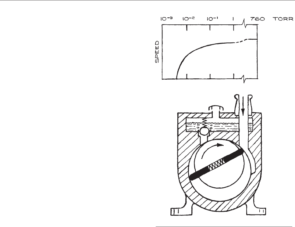
vacuum it is common practice to employ pumps with com-
plimentary characteristics in parallel.
Mechanical pumps operating in the rough vacuum
region with ultimate low-pressure limits of 5 torr to 5 mtorr
serve two important functions in attaining high and ultra-
high vacuum. A pump that will achieve a high vacuum at
its inlet will invariably have a maximum tolerable outlet
pressure; this is the critical backing pressure. A mechan-
ical pump is employed to maintain the high-vacuum pump
exhaust pressure below the critical pressure and in this
function the mechanical pump is referred to as a backing
pump or forepump. In addition, it is necessary for the
pressure in a vacuum chamber to be below some pressure
before the high-vacuum pump can be put into operation;
this pressure is sometimes referred to as the stall pressure.
A mechanical pump is used to attain this maximum start-
ing pressure in the chamber and in this function the pump
is referred to as a roughing pump.
3.4.1 Mechanical Pumps
Oil-Sealed Rotary Vane Pumps. The pump most
commonly used for attaining pressures down to a few
millitorr is the oil-sealed rotary vane pump shown
schematically in Figure 3.8. In this pump a rotor turns
of
f-center within a cylindrical stator. The interior of the
pump is divided into two volumes by spring-loaded vanes
attached to the rotor. Gas from the pump inlet enters one of
these volumes and is compressed and forced through a one-
way valve to the exhaust. A thin film of oil maintains the
seal between the vanes and the stator. The oil used in these
pumps is good-quality hydrocarbon oil from which the
high-vapor-pressure fraction has been removed. These
pumps are also made in a two-stage version in which two
pumps with rotors on a common shaft operate in series.
Rotary pumps to be used for pumping condensable vapors,
water vapor in particular, are provided with a gas ballast.
This is a valve that admits air to the compressed gas just
prior to the exhaust cycle. This additional air causes the
exhaust valve to open before the pressures of condensable
vapors exceed their vapor pressure and thus prevents these
vapors from condensing inside the pump.
Oil-sealed rotary vane pumps will operate for years
without attention if the inner surfaces do not rust and the
oil maintains its lubricating properties. It is wise to leave
these pumps operating continuously so that the oil stays
warm and dry. In use, an increase in the lowest attainable
pressure (the base pressure) indicates that the oil has been
contaminated with volatile materials. The dirty oil should
be drained while the pump is warm. The pump should be
filled with new oil, run for several minutes, drained, and
refilled with a second charge of new oil. For storage, a
pump should be filled with new oil and the ports sealed.
Rotary pumps are av aila ble with capacities of 1 to 500
Ls
1
.Asingle-stagepumpisusefuldownto50mtorr,anda
two-stage pump to 5 mtorr . Typical perfo rmance of a single-
stage pump is indicated by the pumping-speed curve in Fig-
ure
3.8. A two-stage pump is to be preferred as a backing
pump
for a diffusion pump. W ith a two-stage pump, a base
Figure 3.8 Oil-sealed rotary vane pump.
VACUUM PUMPS 105
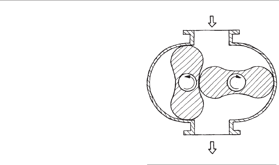
pressure of 10
4
torr can be achieved after a long pumping
time, if the back diffusion of oil vapor from the pump is
suppressed by use of a sorption or liquid-air trap on the pump
inlet. This is a simple scheme for evacuating small spe-
ctrometers and Dewar flasks or other vacuum-type thermal
insulators.
The exhaust gases from an oil-sealed mechanical vac-
uum pump contain a mist of fine droplets of oil. This oil
smoke is especially dense when the inlet pressure exceeds
100 torr. The oil droplets are extremely small, usually less
than 5 microns. Over the course of time, this oil settles on
the pump and its surroundings, and collects dirt and grime.
Furthermore, breathing the finely dispersed oil may injure
the operator’s lungs. In addition, over the course of weeks
or months, this oil represents a significant loss from the oil
charge in the pump, so a pump failure may result if the oil
level in the pump is not faithfully monitored. Most pump
manufacturers market filters that cause the exhaust oil mist
to coalesce and run back into the pump; their use is rec-
ommended. In addition, modern standards of laboratory
hygiene require venting a mechanical pump into the labo-
ratory fume hood. If toxic gases are being pumped it is of
course essential to pipe the exhaust out of the lab. Some-
times, a pretreatment involving passage of the exhaust
through a neutralizing chemical bath is required. In most
cases exhaust lines can be made of PVC drainpipe avail-
able from plumbing suppliers. The exhaust line should rise
vertically from the pump so that oil in the exhaust will
collect on the walls of the line and run downward back
to the pump. An exception to this scheme arises in the case
of a wet vacuum process. If considerable water is exhausted
from the pump, there is the danger that water will condense
in the exhaust line and run back into the pump.
Roots Blowers. A Roots blower is a displacement
pump. As illustrated in Figure 3.9, these pumps consist of
a
pair of counter-rotating two-lobed rotors on parallel shafts.
Rotational speeds are about 3000 rpm. There is a clearance
of a few thousandths of an inch between the rotors
themselves and between the rotors and the housing. A
volume of gas is trapped at the inlet and compressed as it
ismovedtotheexhaust.Thereisnooilinthebodyofthe
pump to maintain a high-pressure seal, but, owing to the high
speed of the rotors, a compression ratio as great as 40:1 can
be achiev ed. The virtue of the Roots blower is its relati v ely
high pumping speed in the 1 to 10
3
torr region. To achieve
an ultimate vacuum of 10
3
torr, a Roots blower is used in
series with a rotary pump at its exhaust. The required speed
of the rotary pump is smaller than that of the Roots pump by
a factor of the in v erse of the compression ratio of the Roots
pump. Roots blowers are available with speeds of a few
hundredtomanythousandL/s.
Piston Pumps. There are now available piston pumps
with Teflon-sealed pistons that do not contaminate the va-
cuum en vironment with oil, as do oil-sealed rotary pumps.
The Leybold EcoDry pump employs a novel diaphragm
exhaust valve that permits a higher compression ratio than
pumps with poppet valv es. The low-pressure limit of these
pumps is about 50 mtorr. Piston pumps are robust and
reliable, but they are also relativ ely expensiv e in com-
parison to rotary pumps. They find use as backing pumps
for pumps such as turbomolecular pumps, when con-
tamination with hydrocarbons is not permissible.
Diaphragm Pumps. Diaphragm pumps are displace-
ment pumps employing the flexure of a thin metal or Teflon
Figure 3.9 Roots blower.
106 VACUUM TECHNOLOGY
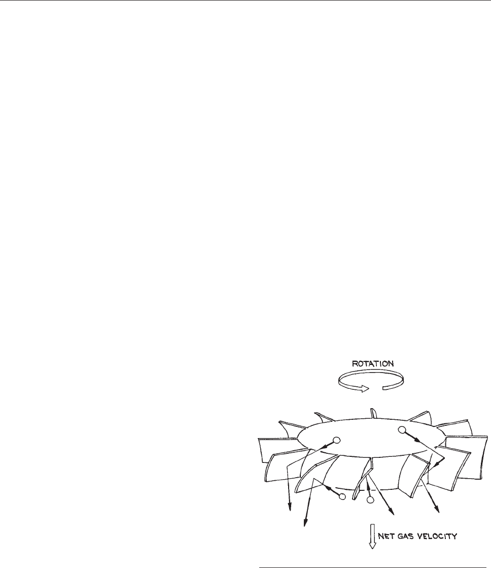
diaphragm to compress gas and drive it out through an
exhaust valve. These are small pumps of low pumping
speed and relatively modest ultimate vacuum. The low
pressure limit is typically about 0.3 torr. Diaphragm
pumps can be made completely free of hydrocarbons so
they are used as roughing pumps and, in some
applications, as backing pumps in ultraclean systems.
Molecular Drag Pumps. A molecular drag pump
incorporates a rotating cylinder within a closely fitting,
stationary cylinder. The clearance between rotor and
stator is of the order of 0.01 in. Pumping occurs when
the surface velocity of the rotor approaches the velocity
of the molecules being pumped, so that molecules striking
the rotor acquire a significant velocity component
tangential to the rotor – they are dragged along with the
rotor. Tangentially accelerated gas molecules rebounding
to the stator are decelerated: they ‘‘pile up,’’ thus yielding
compression. The process is repeated continuously around
the gap between rotor and stator. Helical grooves on the
surface of the rotor or stator direct the flow of continually
compressing gas toward the pump outlet. Drag pumps
provide efficient pumping at inlet pressures from nearly
1 torr down to about 10
6
torr. The compression ratio
for air (that is, the ratio of outlet to inlet pressure) is
typically 10
7
at the low-pressure end of this range. As a
consequence, the exhaust pressure, that is, the critical
backing pressure, falls in the 1 to 10 torr range. The
practical result is that a very small pump is required to
transfer the drag pump throughput to the atmosphere.
Small diaphragm pumps serve well as backing pumps for
molecular drag pumps.
The chamber pressure at the inlet must be below about
1 torr for a drag pump to begin to operate efficiently; a
roughing pump is necessary. The backing pump, pumping
through the drag pump, can serve to rough down the cham-
ber, however, the gap between rotor and stator is small and
restrictive in the viscous-flow regime. A separate roughing
pump or a bypass (with a valve) from the chamber to the
backing pump should be provided.
Molecular drag pumps provide modest pumping speeds
at high vacuum – the inlet apert ure is effectively the gap
between rotor and stator. Drag pumps are currently avail-
able with pumping speeds of up to about 30 L/s. The great
virtue of the drag pump is the relatively high throughput in
the 1 to 10
3
torr pressure range. Displacement pumps such
as rotary-vane pumps, piston pumps, and Roots blowers, lose
efficiency below 0.1 torr. High-vacuum pumps such as dif-
fusion pumps, turbomolecular pumps, and ion/getter pumps,
‘‘stall’’ at pressures abov e 0.01 torr. If pumpdo wn time is an
important issue, a molecular drag pump may be a good
choice for a small vacuum system with an ultimate pressure
of 10
6
torr. With a 1 L s
1
roughing/backing pump and a
drag pump of 30 L s
1
, a volume of 100 L can be evacuated
to less than 10
4
torr in a matter of minutes.
Turbomolecular Pumps. Turbomolecular pumps
operate in the molecular-flow regime. The construction is
similar to that of an aircraft-type jet turbine engine. A
series of bladed turbine rotors on a common shaft turn at
20 000 to 90 000 rpm. The edge speed of a rotor
approaches molecular velocities. The rotor blades are
canted so that a molecule striking a blade receives a
significant component of velocity in the direction of the
pump exhaust (Figure 3.10). Bladed stators are interleaved
between
the rotors. The stator blades are canted in the
opposite direction from that of the rotors in order to
decelerate the molecules and compress the flowing gas
before it is delivered downward to the next rotor–stator
pair. These pumps provide roughly the same pumping
speed for all gases; however, the compression ratio
Figure 3.10 Rotor of turbomolecular pump.
VACUUM PUMPS 107
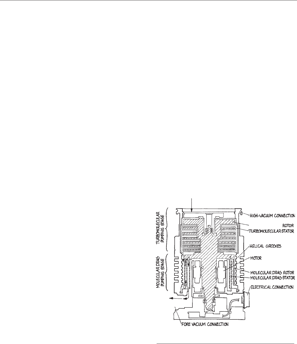
depends upon the nature of the gas being pumped. A single
rotor–stator pair typically provides a compression ratio of
about 10 for N
2
. To a first approximation, the logarithm
of the compression ratio is proportional to the square root
of the molecular weight of the gas; thus, for example, a
multistage pump with eight rotors may have a compression
ratio of 10
8
for N
2
, but only 10
2
to 10
3
for H
2
. A desirable
consequence of the strong dependence upon molecular
weight is that the compression ratio is very high for oil
vapor backstreaming from the pump bearings or from the
pump exhaust; thus a turbopump provides an essentially
oil-free vacuum. The compression ratio is extremely
sensitive to the pressure at the outlet of the pump. A
typical turbopump may have a compression ratio of 10
8
for air if the pressure at the exhaust is maintained below
0.1 torr, but if the exhaust pressure rises to 1.0 torr, the
compression ratio falls to 10.
A turbomolecular pump is usually run in series with a
conventional oil-sealed rotary pump as a backing pump.
The backing pump also serves as a forepump. With the
vacuum chamber at atmospheric pressure, the rotary pump
is activated to evacuate the chamber, drawing gas directly
through the body of the turbopump. Depending on the
manufacturer’s specification, the turbo is activated at the
same time or somewhat later as the chamber pressure falls
so that the turbo is coming up to its operating speed as the
chamber pressure reaches a pressure of a few millitorr.
The critical elements of a turbomolecular pump include
the motor and the bearings. Typically, 400 Hz synchronous
motors are used. Active electronic control is employed to
maintain rotor speed over a wide range of loads and to
protect the pump in the event of an overload. The motor
driver and control represent a significant fraction of the
total cost of a turbomolecular pumping system. Many tur-
bopumps use water-cooled, grease-packed bearings. Some
use oil as a bearing lubricant with the oil being circulated
to a water-cooled heat exchanger. Magnetic suspension
systems are the most recent development (Balzers, Osaka,
and Varian). There is no mechanical contact in a magnetic
bearing; there is essentially no friction and lubrication is
unnecessary. In some pumps the rotor is completely mag-
netically suspended, while in others a magnetic bearing is
used at the inlet end of the rotor with a conventional
grease-lubricated bearing at the outlet, relying upon the
high pumping speeds for hydrocarbons to suppress oil
backstreaming. Axial and radial magnetic fields to support
the rotor are provided by electromagnets in a feedback
system that senses the position of the rotor and makes
corrections to offset disturbing forces. A mechanical bear-
ing is provided to catch the rotor in the event of catastrophic
imbalance and to support the rotor when the pump is not in
operation. A backup electrical system is required to protect
against a sudden loss of power to the magnet system when
the pump is in operation. This may be simply a battery,
however, in sophisticated systems, the pump motor is oper-
ated as a generator when external power is lost, in order to
provide electricity for the magnetic bearings.
The most recent innovation is a compound pump design
incorporating a multistage turbomolecular pump mounted
on a common axis above a molecular drag pump, as shown
in Figure 3.11. These are sometimes called hybrid pumps
or
compound turbomolecular drag pumps; a complete
system effectively has three pumps operating in series: a
turbomolecular pump, a molecular drag pump, and a
displacement-type backing pump (Balzers). The hybrid
arrangement increases the compression ratio of the high-
vacuum pumping stage by several orders of magnitude,
with a concomitant increase in the outlet pressure.
Figure 3.11 Compound turbomolecular/molecular drag
pump.
108 VACUUM TECHNOLOGY

The tolerable backing pump pressure of a hybrid pump is
in the 1 to 10 torr range. With the increase in outlet pres-
sure comes a corresponding decrease in the volume flow
rate at the exhaust. The important consequence is that
these pumps require only a small dry-diaphragm backing
pump that, with the inclusion of a magnetic rotor suspen-
sion, creates an ultrahigh vacuum pumping system that is
completely free of hydrocarbons. Complete turnkey sys-
tems are available that include a compound pump with a
motor controller, a backing pump, and all necessary inter-
locks to control startup and shutdown. Pressures below
10
10
torr are attainable.
The hi gh rotationa l speeds and close tolera nces in a
turbomolecular pump place a p rem ium upon careful
mounting, cleanli ness , and proper mainte na nce. Owing
to the very small clearances between moving and station-
ary components, twisting and bending forces that would
cause distortion cannot be applied to the pump body. The
pump should not be used as the mounting platform for the
vacuum system. The pump should be suspended by its
inlet flange. Small particles can have disastrous effects
upon bearings and rotors at high speeds. The vacuum
container pumped by a turbopump must be kept scrupu-
lously clean. A protective screen, known as a splinter
shield, over the inlet is essential. W hen the vacuum con-
tainer is to be let up to at mosph eric pressure, gas should
be admitted slowly so that turbulence d oes not carry deb-
ris into the turbopump.
Careful and systematic startup and shutdown procedures
are essential to protect the turbopump and to exclude oil
from the vacuum system. As mentioned above, turbos are
usually operated without a valve at the inlet, however, a
valve is required in the foreline between the turbo outlet
and its backing pump. At startup with the turbo and the
vacuum system at atmospheric pressure, the backing pump
is activated and the foreline valve is opened. The rush of
dense gas into the backing pump prevents oil from back-
streaming. As the pressure falls, the turbo activation is
timed so that the turbo is up to at least 50% of its maximum
speed before the pressure at the pump inlet falls below a
few hundred millitorr. At this point the turbo compression
should be sufficient to prevent oil vapor from backstream-
ing to the vacuum system. At shutdown, the foreline valve
is closed immediately after power is cut from the turbo.
The vacuum system should be vented before the rotor falls
below 50% of its maximum speed – again so that the
compression ratio is sufficient to prevent backstreaming
of oil from the bearings. When the pressure has risen above
several hundred torr, backstreaming is essentially impos-
sible. It follows that a pump that is not operating should not
be stored under vacuum. It also should be emphasized that
the pump must be vented above the outlet. Many manu-
facturers sell turbopumps and controllers as a complete
system that incorporates the necessary valves and timing
circuits to automatically perform the startup and shutdown
procedures.
A turbomolecular pump offers many advantages for
high- or ultrahigh-vacuum systems. Of course these must
be weighed against the disadvantages, the main one being
the relatively high initial cost and the cost of major servic-
ing; a complete turbomolecular-pump system may cost
two or more times as much as a comparable diffusion-
pump system. Turbomolecular pumps with pumping
speeds from 10 to 1000 L/s are available. A turbopumped
system can achieve pressures below 10
10
torr. Most gases
can be pumped, although, as noted, turbos do not effi-
ciently pump hydrogen and helium. Most corrosive gases
are acceptable, providing the bearing lubricant does not
come under attack. Turbopumps are compact and rela-
tively light in weight; they need not be mounted on the
underside of a vacuum system. For many types of pumps,
the mounting orientation is not critical – these can be
mounted with the axis horizontal. Turbos can be baked
to reduce outgassing; many are equipped with heating
jackets for this purpose. A turbo can be used on a system
that is to be baked, provided the inlet temperature does not
exceed 100 – 120 ºC. Magnetic fields can be a problem, as
eddy currents induced in the aluminum rotor assembly
cause heating. The specification for most pumps calls for
magnetic fields not to exceed 50 to 100 gauss at the inlet. A
turbomolecular pump can run for one to three years with-
out attention. The major maintenance procedure usually
involves replacing the bearings and rebalancing the rotor.
These procedures often require the pump to be returned to
the manufacturer.
3.4.2 Vapor Diffusion Pumps
In a diffusion pump, gas molecules are moved from inlet to
outlet by momentum transfer from a directed stream of oil
VACUUM PUMPS 109
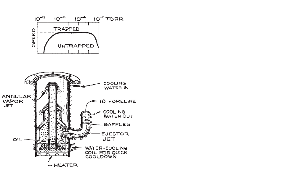
or mercury vapor. As shown in Figure 3.12, the working
fluid is evaporated in an electrically heated boiler at the
bottom of the pump. Vapor is conducted upward through
a tower above the boiler to an array of nozzles from which
the vapor is emitted in a jet directed downward and outward
toward the pump walls. The walls of the pump are cooled,
so that molecules of the working-fluid vapor condense
before their motion is randomized by repeated collisions.
The diffusion pump walls are usually water-cooled,
although in some small pumps they are air-cooled. The
condensate runs down the pump wall to return to the boiler.
Efficient operation of a diffusion pump requires a temper-
ature gradient from top to bottom. The pump wall should
be lowest at the top of the pump – less that 30 ºC–to
effectively condense oil vapor, and highest at the bottom
to drive absorbed gas out of the oil condensate. For this
reason the cooling water flows from top to bottom and the
flow rate is regulated; too high a flow rate results in too low
a temperature at the bottom of the pump.
Because the pumping action of a diffusion pump relies
on momentum transferred in collisions between the mole-
cules of the working fluid vapor and the molecules being
pumped, the speed of the pump is greater for light gases
than for heavy gases. The inlet area essentially determines
the net speed of the pump. For air the pumping speed is
about 4 L s
1
cm
2
of inlet area.
As indicated by the pumping-speed curve in Figure 3.12,
the
pumping action of a diffusion pump begins to fail when
the inlet pressure increases to the point where the mean
free path of the molecules being pumped is less than the
distance from the vapor-jet nozzle to the wall. When this
occurs the net downward momentum of vapor molecules is
lost and the vapor begins to diffuse upward into the vacuum
system. Diffusion pumping of a vacuum chamber may be
initiated at 50 to 100 mtorr, but the system pressure should
quickly fall below 1 mtorr or the chamber will become
significantly contaminated with the vapor of the working
fluid. Oil diffusion pumps can run against an outlet pres-
sure of 300 to 500 mtorr, and mercury pumps can tolerate
an outlet pressure of a few torr. A backing pump, usually
an oil-sealed rotary pump, is required. The speed of the
diffusion pump is insensitive to foreline pressure up to
some critical pressure. If this critical backing pressure is
exceeded, the pump is said to stall. This is a disaster,
because hot pump-fluid vapor is flushed backwards through
the pump into the chamber. The usual practice is to maintain
the oil-diffusion-pump foreline pressure below 50 mtorr.
The primary difficulty with diffusion pumps is the back-
streaming of oil vapor from the pump inlet. Without appro-
priate precautions this can amount to as much as a
microgram per minute for each cm
2
of pump inlet area.
Backstreaming is much worse if the foreline pressure of a
hot pump accidentally rises above the critical backing
pressure of a few hundred millitorr. It is essential to main-
tain the pump cooling system. Most diffusion pumps are
water-cooled. A filter in the cooling-water line is necessary
to reduce the possibility of clogging. Cooling water should
enter at the top of the pump so that the uppermost part of
the pump wall is at the lowest temperature. The next line of
defense is a ‘‘cold cap’’ typically consisting of a conical
shield over the top of the jet tower. The cold cap is cooled
by water flow or by solid thermal contact with the pump
body. Diffusion pumps usually are supplied with a cold cap
installed. In most installations a water- or refrigerant-
cooled baffle ( Figure 3.26) is mounted on top of the pump.
The
cold cap and baffle together reduce backstreaming by
Figure 3.12 Diffusion pump.
110 VACUUM TECHNOLOGY

as much as three orders of magnitude with a loss of pump-
ing speed of perhaps 50%. For many purposes, the vacuum
above the baffle can be considered oil-free. Oil can reach
the vacuum chamber as a liquid film that creeps up the
walls above the pump. To eliminate this problem, an anti-
creep barrier consisting of an annular ring made of Teflon,
a material not wetted by oil, can be installed on top of the
baffle. The ultimate performance and the cleanest vacuum
are obtained with the installation of a liquid-nitrogen-
cooled trap (Figure 3.25) above the baffle.
The
properties of diffusion-pump fluids are given in
Table 3.3; included are hydrocarbon, perfluorocarbon and
silicone
oils, and mercury. The various diffusion pump oils
can be used interchangeably in an oil diffusion pump. The
choice depends upon the desired ultimate pressure, the
demands of the particular application, and the cost. The
matter of economics is significant; the cost of the oils listed
in Table 3.3 ranges over more than a factor of 20. The
perfluorocarbon
and polyether oils are sufficiently costly
that it is economical to reclaim them; many vacuum hard-
ware companies offer this service. The absolute lowest
pressure attainable with an untrapped diffusion pump is
the room-temperature vapor pressure of the working fluid.
The silicone oils are the least expensive of the high-per-
formance (i.e., low ultimate pressure) pump fluids. They are
exceptionally resistant to oxidation and chemical attack,
except in the presence of BCl
3
and, to a lesser extent, CF
4
and CCl
4
. The main drawback to silicone oils is that the
residue of backstreaming oil found on surfaces in the vacuum
system will decompose and polymerize to produce insulating
films upon exposure to heat and charged-particle bombard-
ment; silicone oils are unsuitable for diffusion pumps on
instruments such as mass spectrometers or electron micro-
scopes. The phthalate and sebacate oils are ine xpensi v e flu-
ids suitable for many applications. Decomposition of these
hydrocarbon oils yields carbonaceous deposits that are con-
ductiv e. Polyphenylether oils of fer exceptional chemical and
thermal stability. These are well suited for use with mass
spectrometers and other charged-particle-beam instruments.
The perfluorocarbon oils are suitable for pumping corrosive
gases, with the exception of Lewis acids such as BCl
3
and
AlF
3
. Their performance under charged-particle bombard-
ment is probably the best of all pump fluids.
Mercury diffusion pumps find only a few specialized
uses that rely upon the chemical inertness of mercury
vapor. They are occasionally used on mass spectrometers
because of the simple, easily identified spectrum of mer-
cury vapor. Mercury diffusion pumps are most often made
of Pyrex glass and are intended for use with glass vacuum
systems used to handle and distill small quantities of
volatile chemicals. Mercury diffusion pumps tolerate inlet
pressures 10 times greater than the maximum inlet pres-
sure tolerated by oil pumps. In addition the critical foreline
pressure for a mercury pump is much higher. Because the
room-temperature vapor pressure of mercury is about 10
3
torr, an inlet cold trap is required to prevent bulk migration
of mercury into the vacuum system. Mercury vapor is
toxic, and care must be taken to properly trap and vent
the backing-pump exhaust.
Table 3.3 Properties of diffusion-pump fluids
Trade Names
(chemical composition)
Boiling
Point at
1 torr
(ºC)
Approximate
Vapor
Pressure
@20 ºC
(torr)
(Mercury) 120 2 3 10
3
(Di-n-butyl phthalate) 140 2 3 10
5
Octoil, Diffoil
(di-2-ethylhexylphthalate)
200 3 3 10
7
Octoil-S, Diffoil-S
(di-2-ethylhexylsebacate)
210 3 3 10
8
Convoil-20
(saturated hydrocarbon)
190 5 3 10
7
Neovac Sy
(alkyldiphenylether)
240 1 3 10
8
Convalex-10
(polyphenyl ether)
280 7 3 10
10
Santovac-5
(pentaphenyl ether)
280 5 3 10
10
D.C.704
(tetraphenyl tetramethyl
trisiloxane)
240 3 3 10
8
D.C.705
(pentaphenyl trimethyl
trisiloxane)
250 5 3 10
10
FomblinY-VAC 25/9
(perfluoropolyether)
230 2 3 10
9
Krytox1625
(perfluoropolyether)
250 2 3 10
9
VACUUM PUMPS 111

Diffusion pumps with speeds of 50 to 50 000 L/s and
with nominal inlet port diameters of 2 to 100 cm are avail-
able. Diffusion pumps are constructed of Pyrex glass, mild
steel, or stainless steel. The jets and towers of pumps with
steel barrels are aluminum. The choice of glass or steel
usually depends upon the material that is used to construct
the vacuum container, although it is also relatively simple
to mate glass to steel with an elastomer gasket or through a
metal-to-glass seal. For those systems that are intended to
handle reactive gases, glass is the preferred material; how-
ever, glass pumps are available only in small sizes.
Diffusion pump maintenance involves assuring the qual-
ity and quantity of the pump fluid and checking that the
heaters are operating. Some reaction of the pumped gas
with the pump fluid is inevitable, so periodic inspection
of the pump innards is essential. Moderate discoloration
of the oil is not significant, however, if the oil is opaque it
should be replaced. The interior of the pump must be thor-
oughly cleaned before adding new oil, especially if a differ-
ent type of oil is being installed. Scrubbing with acetone,
followed by an acetone and an ethanol rinse will remove
hydrocarbon oils and, with persistence, silicone oils. Depos-
its of badly decomposed oil can be removed with naphtha-
lene. Polyphenylether oils are soluble in trichloroethylene
and 1,1,1-trichloroethane. Both these solvents should be
used with care in a well-ventilated environment. Fluorocar-
bon oils are soluble in fluorinated alkanes such as trichlor-
otrifluoroethane and perfluorooctane. Severe decomposition
of the oil results in black, carbonaceous deposits on the jet
tower. These must be removed mechanically by scrubbing
with fine abrasi ve or by glass-bead blasting. The tower must
be carefully cleaned before reinstallation in the pump.
There is a close fit between the tower and the pump body.
A residue of abrasive cleaning materials will result in the
tower becoming jammed in the pump body.
Diffusion pumps use flat ‘‘pancake’’ heating elements
bolted to the bottom of the pump or cylindrical ‘‘cartridge’’
heaters inserted in close-fitting holes in the bottom of the
pump. As many as six cartridge heaters wired in parallel
may be used. The advantage to multiple heaters is that the
pump continues to operate if one or more heaters burn out,
albeit with some loss of efficiency. On the other hand, the
loss of one or more heaters may go unnoticed until signifi-
cant contamination of the vacuum has occurred. The indi-
vidual cartridge heaters may be disconnected from one
another and individually checked for electrical continuity.
It is essential that diffusion pump heaters be in good ther-
mal contact with the pump over their entire mating surfa-
ces or the heaters will burn out prematurely. A coating of
‘‘milk of magnesia’’ (a slurry of MgO in water) will assure
good contact and facilitate removal at a later time by pre-
venting the heater from sticking to the pump because of
corrosion or cold welding.
A diffusion-pumped system is the most economical
route to high and even ultrahigh vacuum in chambers of
moderate size. With no moving parts and no critical
dimensions, diffusion pumps are robust and long-lived.
Decades-old pumps can be perfectly serviceable. This is
a boon for researchers on a limited budget, since used
pumps are available at little or no cost.
3.4.3 Entrainment Pumps
A variety of vacuum pumps remove gas from a system by
chemically or physically tying up molecules on a surface
or by trapping them in the interior of a solid. Two of the
principal advantages of these pumps are that they require
no backing pump and they contain no fluids to contaminate
the vacuum.
Sorption Pumps. The simplest of the entrainment
pumps is the sorption pump ill ustrated in Figure 3.13.
The
sorbent material is activated char coal or one of the
synthetic zeolite mater ials k nown as molecular sieves.
These ma ter ial s are effective sorbent s partly be ca us e of
their huge surface area – of the order of thousands of
square meters per gram. The most common molecular
sieves are zeolite 5A o r 13X. The number in the sieve
code specifies the pore size: 5A is preferred for air
pumping, while 13X is used for trapping hydrocarbons.
All of these materials will pump water and hydrocarbon
vapors at room te mpe ratur e, but they must be cooled
to liquid-nitrogen temperature to absorb air. Sorbe nt
materials do not trap hydrogen or helium at liquid-
nitrogen temperature. Without some a uxiliary means of
removing hydrogen and helium, the partial pressures of
these gases in a system will establish the lowest attainable
pressure. Sorption pumps must be provided with a poppet
valve becaus e the sorbent materi al releas es all of its
absorbed air as it warms to room temperature.
112 VACUUM TECHNOLOGY
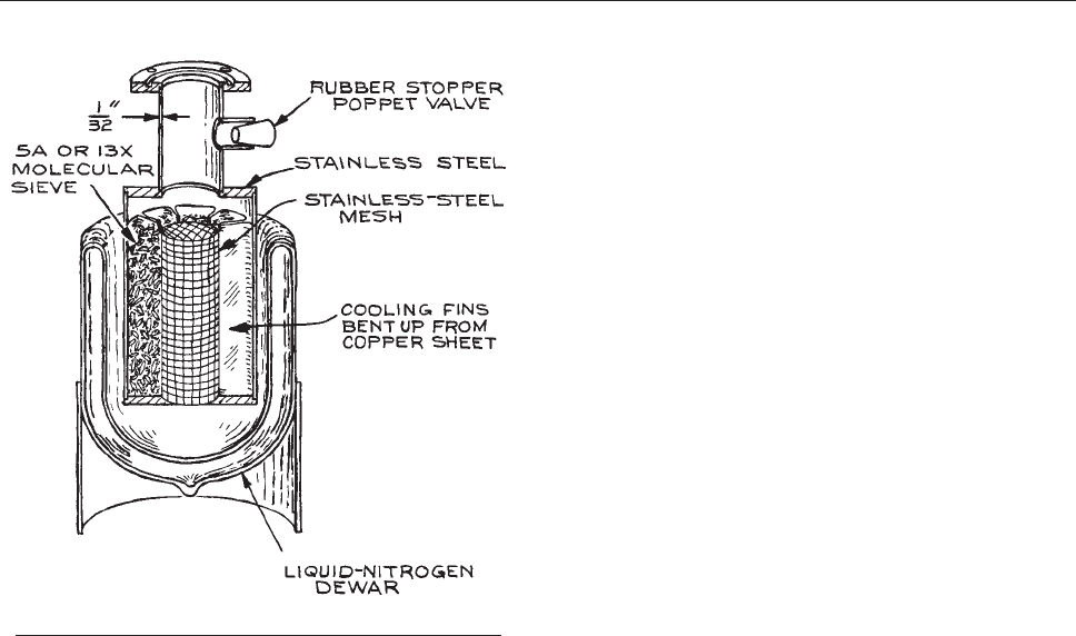
The sorbent is initially activated by baking to 250 ºC.
After several pumping cycles the pores of the sorbent
material will become clogged with water and the efficiency
of the pump will deteriorate. Water is removed by baking
the pump to 250 ºC with the poppet valve open and then
cooling to room temperature with the valve closed so that
moisture from the room is not reabsorbed. Baking can be
accomplished by wrapping the pump with heating tape.
Custom-made heating mantles can be obtained inexpen-
sively from the Glas-Col Company.
In a well-designed pump, 1 kg of dry Linde 5A molec-
ular sieve will pump a 100 L volume from atmosphere to
less than 10
2
torr in about 20 minutes. The pump must be
designed to provide good thermal contact between the
sieve and the coolant to obtain the maximum pumping
speed. A thin-walled inlet tube will minimize heat conduc-
tion into the pump. Sorption pumps similar to that in the
figure are available from suppliers of vacuum hardware.
Pressures below 10
6
may be attained in a system that has
been roughed down. A simple way to achieve low pres-
sures with sorption pumping is to use two or three pumps
on a manifold. Each pump is equipped with a shutoff valve.
Starting at atmospheric pressure, one pump valve is opened
to rough down the system. This pump should be of a size
such that the pressure falls to less than 1 torr. This pump is
valved off and the next pump is brought on line and so on.
To attain the lowest possible pressure with this arrange-
ment, the vacuum chamber can be purged of hydrogen
and helium before ev acuation proceeds. This can be accom-
plished by flushing the vacuum chamber with dry air or dry
nitrogen before initiating pumping with the sorption pumps.
Getter Pumps. Clean surfaces of refractory metals
such as titanium, molybdenum, tantalum, or zirconium
will pump most gases by chemisorption. This process is
called gettering. In a getter pump, the active metal surface
is produced in vacuo. Titanium or a titanium/molybdenum
alloy is the preferred metal. A getter pump employing a
freshly evaporated titanium surface is called a titanium
sublimation pump. At room temperature a titanium
surface pumps H
2
,N
2
,O
2
,CO
2
, and H
2
O at rates of
several L/s per cm
2
of exposed surface. Cooling the
surface to liquid nitrogen temperatures may double or
triple the pumping speed for N
2
and H
2
. Methane and
the noble gases, such as Ar and He, are not pumped at all.
A titanium sublimation pump consists of a titanium sub-
limator and the surface surrounding the sublimator. The
surface may or may not be cooled. These pumps operate
effectively between 10
3
and 10
11
torr, however, the inert
gases must be removed before ultrahigh vacuum can be
achieved. This can be accomplished with a small ion pump
in parallel with the getter pump. An alternative method to
(at least initially) remove rare gases is to purge the system
with pure dry nitrogen prior to evacuation. The titanium
surface must be renewed at a rate roughly equal to the rate
at which a monolayer of gas is adsorbed. Down to about
10
7
torr the titanium surface is continuously deposited.
Below 10
7
torr the titanium need only be deposited peri-
odically. The capacity of a titanium sublimation pump is
about 30 torr L per gram Ti. A forepump is not required,
but a mechanical or sorption roughing pump is needed to
reach a starting pressure of about 10
3
torr.
Titanium sublimation pumps are quite simple in design
and correspondingly inexpensive. Commercially available
sublimators consist of two to four electrical feedthroughs
in a flange with titanium filaments suspended between the
Figure 3.13 Sorption pump.
VACUUM PUMPS 113
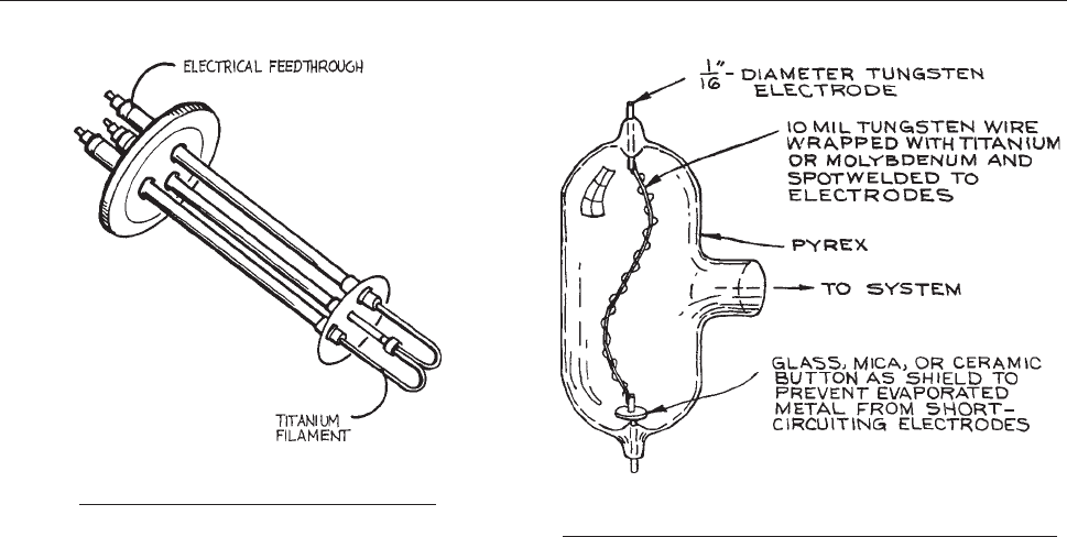
feedthroughs, as illustrated in Figure 3.14. A controller
supplies electrical current through the filaments at a rate
appropriate for the vacuum conditions. The sublimator can
be inserted in a side arm on the vacuum system with baffles
or an elbow arranged to prevent titanium vapor from enter-
ing the main part of the vacuum chamber. The walls of the
sidearm then serve as the pump. The pumping speed with
this arrangement will usually correspond to the conduc-
tance of the sidearm with its baffles. Vacuum housings with
water- or liquid nitrogen-cooled baffles are available to
contain the sublimator. These are designed to be mounted
directly atop a turbomolecular pump in an ultrahigh vac-
uum system. For a glass vacuum system, a simple pump
can be made by wrapping titanium wire around a tungsten
wire sealed in a glass bulb, as shown in Figure 3.15. The
tungsten
filament is electrically heated to evaporate the
titanium that in turn condenses on the walls of the bulb.
A new class of getter pumps employing so-called ‘‘non-
evaporable’’ getters has recently come into use (see, for
example, SAES Getters, S.p.A.). These employ a porous,
sintered, zirconium alloy that strongly absorbs and reacts
with active gases. The getter is activated by heating to 700
to 900 ºC in vacuo to remove any surface oxide. In oper-
ation the getter is maintained at a temperature of about
400 ºC. CO, CO
2
,N
2
, and O
2
are irreversibly adsorbed.
Water vapor and hydrocarbons are dissociatively adsorbed.
H
2
is reversibly adsorbed; there is no sorption of the rare
gases. Nonevaporable getter pumps operate down to 10
12
torr. The pumping speed is highest for H
2
and H
2
O. These
pumps are an excellent adjunct to a turbomolecular pump
in a UHV system.
Cryopumps. Any surface will act as a pump for a gas
that condenses at the temperature of the surface. A pump
that relies primarily upon condensation on a cold surface is
called a cryopump. Commercial versions of these pumps
employ a closed-circuit helium refrigerator to cool the
active surfaces. Working temperatures are typically
below 20 K. These pumps usually employ two stages. In
the first stage a metal surface is maintained at 30 to 50 K to
trap water vapor, carbon dioxide, and the major
components of air. In some designs a liquid-nitrogen-
cooled baffle to reduce the load of water vapor on the
subsequent stages precedes this first stage. The second
stage, maintained at 10 to 20 K, is coated with a
cryosorbent material such as activated charcoal to
provide pumping of neon, hydrogen, and helium.
Cryopumps provide a high pumping speed for the easily
condensed gases. Their performance with helium depends
critically upon the quality and recent history of the
cryosorbent surface. The gas captured by a cryopump is
Figure 3.14 Titanium sublimator on a
UHV flange.
Figure 3.15 Simple titanium sublimation pump as an
appendage on a glass vacuum system.
114 VACUUM TECHNOLOGY

not permanently bound. The pump must periodically be
warmed to regenerate the pumping surfaces. Because of
the limited capacity of the pump, a roughing pump is
necessary, as is a valve between the cryopump and the
vacuum chamber so that the vacuum system can be
rough pumped to a pressure less than about 10
3
torr
before cryopumping is initiated.
Ion Pumps. An ion pump combines getter pumping
with the pumping action exhibited by an ionization
gauge. Within these pumps a magnetically confined
discharge is maintained between a stainless-steel anode
and a titanium cathode. The discharge is initiated by
field emission when a potential of about 7 kV is placed
across the electrodes. After the discharge is struck, a
current-limiting power supply maintains the discharge
rate at 0.2 to 1.5 A, depending on the size of the pump.
Inert-gas molecules, and other molecules as well, are
ionized in the discharge and accelerated into the cathode
with sufficient kinetic energy that they are permanently
buried. Active gases are chemisorbed by titanium that
has been sputtered off the cathode by ion bombardment
and deposited on the anode.
Ion pumps function between 10
2
and 10
11
torr. A
forepump is needed to reach the starting pressure. Since
ion pumps are completely free of hydrocarbons, an oil-free
rough pump is called for. A well-trapped oil-sealed rotary
pump can be used, but roughing with sorption pumps will
guarantee that the vacuum chamber remains clean. An ion
pump has a limited lifetime of operation due largely to the
rate at which the cathode erodes during operation. The
operational lifetime is an inverse function of pressure.
Under continuous operation at 10
3
torr, the lifetime of a
typical pump is only 20 to 50 hours, whereas operation at
10
6
torr can continue for 20 000 to 50 000 hours (6 yrs).
At ultrahigh vacuum the lifetime is essentially infinite.
Ideally, an ion pump is only operated below 10
5
torr,
but because this pressure is difficult to attain with most
roughing systems, pumping can be initiated at 10
3
torr
provided that the gas load is such that the pressure quickly
falls into the desirable range. Ion pumps are frequently
used in conjunction with titanium sublimation pumps. In
fact, some ion pump designs include an integral sublima-
tion pump. The sublimation pump can serve to lower the
pressure from 10
3
torr to 10
5
torr before power is
applied to the ion pump. At lower pressures the titanium
sublimation pump significantly increases the pumping
speed for getterable gases. To attain the lowest possible
pressures, an ion pump can be baked to at least 300 ºC.
Most pumps are equipped with integral heaters for this
purpose. Baking should be initiated only while the pump
is in operation.
The positive-ion current to the cathode of an ion pump is
a function of pressure; the pump serves as its own pressure
gauge. The power supply and control unit for most ion
pumps includes a pressure readout. This is a significant
consideration in the design of a very small ultrahigh vac-
uum system; the cost of a 1 to 5 L/s ion pump with its
control unit is little more than the cost of an ion gauge
and controller.
Ion pumps require no cooling water or backing pump.
They continue pumping by getter action even if the power
fails. Ion pumps do not introduce hydrocarbon or mercury
vapors into the vacuum. Pumps with speeds from one to
many thousands of liters per second are available. The
limited capacity in the 10
3
torr to 10
5
torr range can
be a disadvantage. Stray magnetic and electric fields may
also present a problem; ion pumps may produce a mag-
netic field of a few gauss at a distance of one inlet diameter.
There may also be a problem with ions escaping the pump;
ion emission can be suppressed by placing a suitably
biased screen above the pump inlet. An ion pump with
controller can cost two to three times as much as a com-
parable diffusion pump with an appropriately sized liquid-
nitrogen-cooled baffle.
3.5 VACUUM HARDWARE
3.5.1 Materials
Glass. Two glasses are used in vacuum work: borosilicate
glass or ‘‘hard glass’’ such as Pyrex or Kimax that is about
70% SiO
2
, and quartz glass that is pure silica. Both
materials have a low coefficient of thermal expansion and
are remarkably resistant to fracture under large temperature
gradients (thermal shock). Borosilicate glass has a broad
softening temperature range allowing glass vacuum
apparatus to be constructed and modified in situ by a
moderately competent glassblower as described in
Chapter 2. Quartz has a very high softening temperature
VACUUM HARDWARE 115

and a narrow softening temperature range and requires a
skillful glassblower. Quartz can be used in continuous
operation at temperatures up to 1000 ºC. Quartz is used
primarily when its high temperature strength or broad
range of optical transmission is to be exploited.
The permeability of helium through quartz is surprisingly
large – about 10
11
torr L s
1
mm cm
2
torr
1
[throughput
(torr L s
1
) through unit thickness (mm) per unit area (cm
2
)
per unit helium pressure differential (torr)] at room
temperature and increasing rapidly with increasing
temperature. This can be a problem with quartz windows
in UHV systems. Even when the permeation of atmospheric
helium is not significant, the permeation of helium through a
quartz window can give rise to false signals when helium
leak-testing.
Hard glass tubing and glass vacuum accessories are
inexpensive. Stopcocks and Teflon-sealed vacuum valves;
ball joints, taper joints, and O-ring-sealed joints; traps; and
diffusion pumps are all easily obtained at low cost. In most
cases only the glassblowing ability to make straight butt
joints and T-seals is required to make a complete system
from standard glass accessories.
Glass pipe and pipe fittings are manufactured for the
chemical industry. A variety of standard shapes, such as
elbows, tees, and crosses, are available in pipe diameters of
1/2 to 6 in. Glass process pipe with Teflon seals can be used
to make inexpensive vacuum equipment for use down to
10
8
torr. Couplings are also available for joining glass
pipe to metal pipe and to standard metal flanges and pipe
fittings so it is easy to make a system that combines glass
and metal vacuum components.
Glass and metal parts can be mated through a graded
glass seal. Typically a graded seal appears to be simply a
section of glass tubing butt-sealed to a section of Kovar
metal tube. In fact, the glass tubing consists of a series of
short pieces of glass whose coefficients of thermal expan-
sion vary in small increments from that of hard glass to that
of the metal. Graded seals are useful for joining glass
accessories such as ion-gauge tubes to metal systems.
Alternatively, a graded seal can be employed to insert metal
hardware, such as a valve or an electrical feedthrough, into
a glass vacuum line. Inexpensive graded seals in sizes up to
5 cm diameter are available from commercial sources.
Windows in vacuum systems are often made of quartz.
For high-vacuum work the window can be sealed to the
vacuum wall with an elastomer gasket or O-ring. For ultra-
high vacuum, the edge of the quartz window is metalized
so that the window can be brazed into a metal flange for
installation in a vacuum wall. Window/flange assemblies
are available from most vacuum equipment suppliers.
Ceramics. Ceramics are used as electrical insulators and
thermal isolators. There are literally hundreds of different
kinds of ceramic materials; two find frequent use in vacuum
apparatus: steatite, a magnesium silicate, and alumina
ceramics containing at least 96% Al
2
O
3
. Fabrication of
parts from these materials requires specialized grinding
equipment not ordinarily immediately available to a
laboratory scientist, however, there are many specialized
shops that provide grinding services under contract.
Standard shapes, such as rod, tubing, plate, and spheres,
are available in alumina (Coors Ceramics Co., McDanel
Refractory Porcelain Co., Industrial T ectonics, Inc.). It is
often possible to design an insulator that incorporates
these simple shapes into a more complex assembly.
Threaded steatite standoff insulators inexpensively avai-
lable from electronics suppliers can be used as structural
elements in vacuum apparatus. Corning produces
MACOR, a machinable ceramic that can be fashioned
into complex shapes with ordinary shop machine tools.
Brass and Copper. Brass has the advantage of being
easily machined, and brass parts can be joined by either
soft solder or silver solder. Unfortunately, brass contains a
large percentage of zinc whose volatility limits the use of
brass to pressures above about 10
6
torr. Heating brass
causes it to lose zinc quite rapidly. The vapor pressure of
zinc is about 10
6
torr at 170 ºC and 10
3
torr at 300 ºC.
Forelines for diffusion pumps are conveniently con-
structed of brass or copper tubing and standard plumbing
elbows and tees. Ordinary copper water pipe is acceptable
for forelines and other rough vacuum applications;
however, oxygen-free high-conductivity (OFHC) copper
should be used for high-temperature and high-vacuum
work. A skilled technician can weld copper.
Stainless Steel. The most desirable alloys for the
construction of high-vacuum and ultrahigh-vacuum
apparatus are the (American AISI) 300 series austenitic
stainless steels, especially type 304 and type 316
116 VACUUM TECHNOLOGY

stainless steels; type 303 is not ordinarily used as it contains
volatile elements added to improve machinability. Stainless
steel is strong, reasonably easy to machine, bakeable, and
easy to clean after fabrication. 304 and 316 stainless steels
are essentially nonmagnetic with magnetic permeabilities
less than about 1.01. Stainless-steel parts may be brazed or
silver-soldered. Low-melting (230 ºC) silver–tin solders are
useful for joining stainless-steel parts in the laboratory;
however, it is best if stainless parts are fused together by
arc welding using a nonconsumable tungsten electrode in
an argon atmosphere. This process, known commonly as
heliarc fusion welding o r tungsten-inert-gas (TIG)
welding, produces a very strong joint, and, because no
flux or welding rod is used, such a joint is ea sily cleaned
after welding . M ost machine shops are p rep ared to d o
TIG welding on a routine basis.
The bulk of commercial vacuum fittings (flanges and
shapes such as te es, crosses, and nipples) are fabricated of
type 304 stainless steel. In additi on, type 304 stainless is
widely used in the milk- and food-processing industry. As
a result, many stock shapes are comme rcially available at
low cost. E lbows, te es , crosses, Ys, and many other fit-
tings in sizes up to a t least 6 in. diameter may be pur-
chased from the Ladish Company or Alloy Products
Company.
Aluminum. Aluminum alloys, particularly the 6000
series allo ys, are used for vacuum apparatus. Aluminum
has the advantage over stainless steel of being lighter and
stiffer per unit weight, and much easier to machine. It is
nonmagnetic. The chief disadvantages of aluminum stem
from it s poros ity and the oxide layer that covers the
surface. The rate of outgassing from aluminum is five to
ten times greater than for stainless steel. Aluminum can
be ano dized bl ack (black chrome) to reduce reflectivity
in optic al devices, however, a nodizing may significantly
increase outgassing rates. Welds in aluminum are not
as reliable as welds in stainless and tend to outgas
volatile materials that have been occluded in the weld;
nevertheless, welded aluminum vacuum c ontainers are
used down to at least 10
7
torr. The hard oxide layer
that forms instantl y on a clean aluminum surface is an
electrical insu lator. Th is insulatin g surface tends to
collect electrons or ions to produce an electric field that
is undesirable in some applications. Copper or gold
plating on aluminum or a coating of col loidal graphite
(see Section 5.6.1) should eliminate the accumulation of
s
urface charge.
Plastics. Plastics are used as fixtures, electrical
insulators, bearings, and windows in vacuum systems at
pressures down to 10
7
torr. Their use is limited to varying
degrees because they outgas air, water, and plasticizers,
and because they cannot be heated to high temperatures.
Polyamide (e.g., Nylon) and acetal-resin-based plastics
(e.g., Delrin) are used for mechanical elements in vacuum
systems at temperatures below 100 ºC. These plastics are
hard and machinable. Nylons are self-lubricating and make
excellent bearings. Nylon is hygroscopic and outgasses
water vapor after exposure to air. Outgassing is less of a
problem with Delrin. Windows in vacuum systems may
be made of polymethylmethacrylate (e.g., Plexiglas or
Lucite) or polycarbonate (e.g., Lexan) plastics. Lexan is
especially strong, tough, and machinable, well suited for
use as a structural material or as an electrical insulator.
Fluorocarbon polymers have superior high-temperature
characteristics. Polytetrafluoroethylene (PTFE) (e.g.,
Teflon) can withstand temperatures up to 250 ºC. The
outgassing rate falls below 10
8
torr L s
1
cm
2
after an
initial pumpdown of a day at 100 ºC. Unfortunately, Teflon
is relatively soft, and cold-flows under mechanical
pressure, thus limiting its usefulness as a structural
element. Various polyimides, although expensive, are
finding use in vacuum systems that are to be baked.
Polyetherimide (Ultem) can be used at temperatures to
200 ºC. Polyamide/imide (Torlon) is the highest strength
thermoplastic. Polyimide (Vespel, Kapton) is the ultimate
material for both mechanical elements and electrical
insulation at high temperatures. Vespel has been used
continuously at temperatures approaching 300 ºC in high
vacuum. Polyimide is somewhat hygroscopic, but can be
baked to reduce outgassing. Kapton is polyimide sheet
used for electrical insulation. Kapton-insulated wire is
supplied for high-temperature use in high vacuum and
even ultrahigh vacuum.
A variety of low-vapor-pressure sealers and adhesives
have vacuum applications. Apiezon M grease, Dow-Corning
silicone high-vacuum grease, and FOMBLIN perfluorinated
grease are used to seal stopcocks and ground-glass taper
joints and, in some instances, as low-speed lubricants.
VACUUM HARDWARE 117

Apiezon compounds are used to seal joints and windo ws as
well as to fill small gaps in vacuum systems. These wax-like
materials soften at temperatures of 45 to 100 ºCandhave
vapor pressures between 10
4
and 10
8
torr at room temper -
ature. A variety of resin-based sealers in spray cans are mar-
keted for sealing very small leaks in high-vacuum and e ven
ultrahigh-vacuum systems while they are under v acuum.
Epoxy resins are particularly useful. Epoxy cements
consist of a resin and a catalytic hardener that are com-
bined immediately before use. The proportions of resin
and hardener and subsequent curing must be carefully con-
trolled to prevent excessive outgassing from the hardened
material. Small epoxy kits with resin and catalyst pre-
packaged in the correct proportions are available, as are
silver-filled epoxy formulations that conduct both electric-
ity and heat.
3.5.2 Demountable Vacuum Connections
Vacuum systems require detachable joints for convenience
in assembling and servicing. There are basically three
means of creating a vacuum-tight seal between mating
connectors: pipe threads with a sealant in the joint, elasto-
mer gaskets or ‘‘O’’-rings, and deformable metal gaskets.
Pipe Threads. The threaded parts of a pipe joint are
tapered so that the joint becomes tighter and tighter as the
two are screwed together. The two parts are not made with
sufficient precision to assure a vacuum-tight seal even
though significant distortion of the metal threads can
occur as the parts are joined. To assure a seal, the male
part is covered with a thin layer of Teflon tape prior to
assembly. Teflon thread tape, or thread ‘‘dope,’’ is sold in
hardware stores for use with plumbing fixtures. The tape is
wrapped around the threaded end. No more than two layers
are required and the tape should be stretched as it is wound
on to make a very thin layer. Looking at the end of the male
part, the tape should be wound in a counterclockwise
direction so that the exposed tag end does not get caught
up in the female threads as the joint is assembled. The tape
must be replaced upon reassembly. A significant volume of
gas is trapped in an assembled pipe thread joint. Pipe
thread joints are not appropriate for ultrahigh-vacuum
systems, and their use is to be avoided as much as
possible in high-vacuum systems.
‘‘O’’-Ring Joints. For pressures down to about 10
7
torr, vacuum connections are most often sealed with
rubber O-rings. Several O-ring-sealed joints are illustrated
in Figure 3.16. O-rings are circular gaskets with a round
cr
oss-section. They are available in hundreds of sizes
from 3 mm (.125 in.) I.D. (inner diameter) with a cord
diameter of 2 mm [.070 in. (nominally 1/16 in.)] to 60 cm
(2 ft.) I.D. with a cord diameter of 7 mm [.275 in.
(nominally 1/4 in.)]. Very large rings may be made from
lengths of cord stock with the ends butted together and
glued with cyanoacrylate adhesive (Eastman 910). O-rings
are made of a variety of elastomers. The most common are
Buna-N, a synthetic rubber, and Viton-A, a fluorocarbon
polymer. Buna-N may be heated to 80 ºC and will not
take a set after long periods of compression. Unfortunately
this material outgasses badly, particularly after exposure to
cleaning solvents. Viton-A has a low outgassing rate and
will withstand temperatures up to 250 ºC, but will take
a set after baking. Generally, the advantages of Viton-A
O-rings offset their higher cost.
O-ring-sealed flanges and ‘‘quick connects’’ are easily
fabricated and they are also available ready-made. Mating
flanges have a groove that contains the ring after the
flanges have been pulled into contact with one another.
Usually, one flange is flat and a rectangular-cross-section
groove is cut into the mating flange; flanges can be made
sexless by cutting a groove of half the required depth in
both flanges. Groove design is critical to obtaining a reli-
able seal, as is the surface finish of the flange and inside
the groove. Surface roughness should not exceed 1 lm
(32 microinches). The flange surface and groove should
be cut on a lathe so that tool marks run circumferentially.
Radial scratches are one of the most common causes of
seal failure. To obtain the correct compression of the
O-ring material, the groove depth should be about 80%
of the actual cord diameter for static seals and 85% of
the diameter for dynamic seals. Rubber is deformable,
but incompressible; the width of the groove should be such
that the cross-sectional area of the groove exceeds that of
the O-ring by 30 to 40%. The ID of the groove should
match the O-ring ID; the O-ring is not to be stretched into
its groove. It is sometimes convenient to undercut the sides
of the groove slightly to give a closed dovetail cross-section
rather than a rectangular cross-section, so that the ring is
118 VACUUM TECHNOLOGY
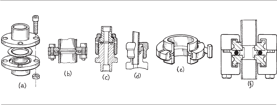
retained in the groove during assembly. For rings up to 30
cm (12 in.) in diameter, the nominal cord diameter should be
3 mm (1/8 in.) or less. Choose a ring to fit in a groove that is
as close to the flange ID as possible, in order to minimize the
amount of gas trapped in the narrow space between the
mated flanges. The bolts or clamps that pull the flanges
together should be as close to the groove as possible to
prevent flange distortion. For static seals, O-rings should
be used dry. Before assembly, the groove should be cleaned
with solvent and the ring wiped free of mold powder with a
dry, lint-free cloth; O-rings should not be cleaned with sol-
vents. For rotating seals a very light film of vacuum grease
on the ring will prevent abrasion. Occasionally a film of
grease may be required on a static O-ring to help make a
seal on an irregular surface. Grease is a liability, however, as
it tends to pick up debris that may disrupt the seal.
For very high temperatures, elastomer O-rings can be
replaced by metal O-rings composed of a thin metal sleeve
with an internal spring to provide resiliency. These are
manufactured by Helicoflex in aluminum, silver, copper,
nickel, and other materials suitable for temperatures from
300 to 600 ºC and in sizes comparable to those of standard
rubber O-rings. The groove design is essentially the same
as for rubber O-rings; detailed design instructions are
available from the manufacturer.
There are three standard types of O-ring sealed joints:
ASA, QF (or KF), and ISO. Examples are shown in Figure
3.
16. The ASA design dates back to an early steamfitters’
st
andard, flange. ASA design consists of two flat flanges
with an O-ring groove in one flange and a circle of bolt
holes well outside of the groove. These flanges are bulky
and require fasteners much larger than needed to resist
atmospheric pressure. The sizing of ASA flanges refers to
the nominal ID of the flange or the nominal OD of the tube
to which it is attached: the bore of a 4 in ASA flange is about
4 in; the OD of the flange is 9 in. Some commercial vacuum
hardware, including large diffusion pumps, large mechani-
cal pumps, and Roots blowers, still use ASA flanges.
The QF (quick flange) or KF (Klein flange) design
employs two, flat, and therefore sexless, flanges with an
outer diameter only slightly larger than that of the O-ring.
The O-ring is mounted around a separate, aluminum ‘‘cen-
tering ring’’ that prevents the O-ring from being forced
inward by external pressure and whose thickness deter-
mines the extent of compression of the O-ring. The center-
ing ring has a lip on both sides that engages the inner
circumference of each flange so that the O-ring is correctly
located on the flanges. A jointed, circular clamp is installed
around the assembled pair of flanges and a thumbscrew is
tightened to draw the two flanges together, compressing
the O-ring. They are compact and, with only a single screw
to tighten, quite convenient to use; a QF fitting can be
assembled with one hand. QF flanges are available in
brass, aluminum, and type 304 and 316 stainless steel in
configurations suitable for a brazed or welded butt joint
or socket joint to tube sizes from 10 mm (1/2 in) to 50 mm
(2 in). A remarkable range of components is available with
QF fittings, including nipples, elbows, tees, 4-, 5-, and 6-
way crosses, as well as adapters to mate QF with other
styles of connectors. In the spirit of ‘‘Tinker Toys,’’ it is
Figure 3.16 O-ring-sealed vacuum connections: (a) an exploded view of an O-ring-sealed flange joint; (b) assembled ASA-style
flange joint; (c) O-ring tube coupling (Cajon VCO); (d) a quick connect; (e) QF(or KF) joint; (f) ISO joint with K-style flanges.
VACUUM HARDWARE 119
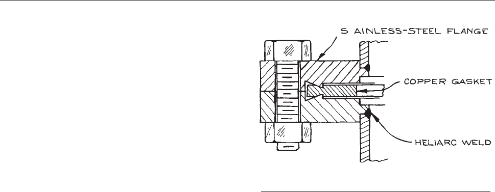
often possible to assemble a large part of a vacuum system
using only these standard components.
ISO flanges are similar to QF flanges but are sized for
larger tubing: nominal bore sizes range from 63 to 630 mm.
The ISO fitting is comprised of two flat flanges with a
combination centering ring and O-ring mounted between
them. The centering ring has a lip on each side that engages
a counterbore near the ID of the flange. ISO flanges are
designed for one of two methods of joining a pair of flanges.
K-style ISO flanges employ clamps that hook over the outer
edges of the mating flanges. F-style flanges have holes for
bolts to draw the two flanges together. K-style flanges are
more compact than F-style flanges. F-style flanges make a
stronger structure appropriate for joining tubing that must
support large transverse forces. An all-metal C-Flex assem-
bly manufactured by EG&G Engineered Products can
replace the centering ring/O-ring assembly in a QF or ISO
joint. These employ a springy, tin-coated, Inconel element
to replace the elastomer O-ring. They can be baked at mod-
est temperatures and are said to be usable at UHV pressures.
The A&N Corporation ULRIC
TM
flange system is similar in
configuration to the ISO flange system and can incorporate a
copper gasket to make a fitting that is bakeable and useable
for ultrahigh vacuum.
Metal Gaskets. Metal sealing materials are required
for ultrahigh-vacuum (UHV). Elastomers are unacceptable
because they outgas and because they cannot be baked
to high temperatures. The ConFlat design developed by
Varian has become the industry standard. Flanges of this
design, now generally known as CF (for ConFlat-
compatible) flanges, are now manufactured by many
vacuum equipment suppliers. The CF sealing system is
composed of two identical flanges and a flat OFHC
copper gasket, as shown in Figure 3.17. Annular knife-
edge
ridges in each flange cut into the gasket to make a
seal as the flanges are drawn together by bolts that pass
through holes in the flanges outboard of the copper gasket.
The entire assembly can be baked to 450 ºC. A great deal
of force is required to make the seal, so many high-tensile-
strength bolts are used, closely spaced around the flange.
The knife-edge is designed so that the correct deformation
of the gasket is obtained when the flanges are drawn into
contact. Careful assembly is important to avoid warping
the flanges. The joint is initially assembled with all the bolts
just finger tight. Then, using good-fitting wrenches and
working in sequence around the flange, each bolt is
tightened no more than one half turn. Going round and
round the flange, the bolts are drawn up just until the
flange surfaces touch. The copper gaskets are permanently
deformed during installation and hence are used only once.
Bolts wear and stretch and must be replaced after perhaps
a dozen assembly cycles. Baking a CF flange encourages
the bolts to seize in their nuts. A very thin coating of
molybdenum disulfide grease helps avoid this problem.
Silver-plated bolts are available to help reduce galling and
seizing in systems that are baked frequently to high
temperatures. CF flanges are specified by the flange OD in
sizes that run from 1.33 in (or 34 mm) to 12 in (305 mm) to
16 1/2 in. These are used with tube sizes from .75 in (or 16
mm in metric sizes) to 10 in (or 250 mm) to 14 in. In UHV
systems, circular cross-section tubes larger than 14 in
diameter are joined with Wheeler flanges that employ a 2
mm diameter OFHC copper wire as a deformable gasket.
Wire-sealed flanges are heavy and very large forces are
required to achieve a seal. They are available from many
manufacturers in sizes up to about 30 in.
3.5.3 Valves
A wide variety of valves are available commercially for use
in glass systems and in high-vacuum and ultrahigh-vacuum
metal systems. Characteristics to be considered in choosing
a valve (roughly in order of importance) include: (i) con-
ductance; (ii) operating temperature; (iii) leak rate around
Figure 3.17 Detail of a bakeable, ultrahigh-vacuum CF
flange.
120 VACUUM TECHNOLOGY
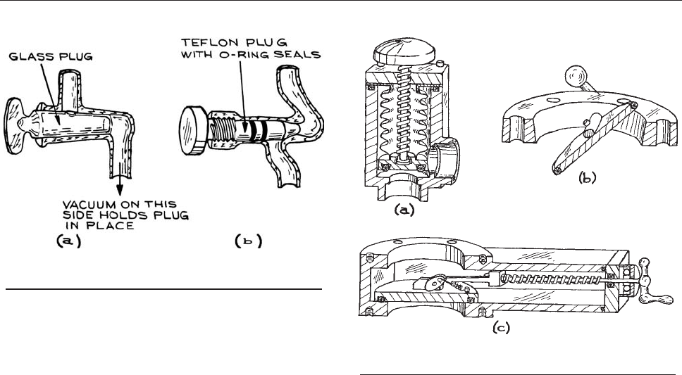
the valve-operating mechanism and the valve seat; (iv)
material of construction [related to (ii)]; (v) configuration;
(vi) cost; (vii) reliability; (viii) ease of maintenance.
Metal valves are always used in metal vacuum systems.
The construction of glass systems is easiest if glass valves
are used; however, glass valves (stopcocks) have relatively
low conductance. The clear passage through an open stop-
cock is typically only a few millimeters in diameter. When
a large-bore, high-conductance, valve is required in a glass
system, a metal valve of suitable size can be inserted using
a glass-to-metal transition on each side of valve. The two
most common glass valves are illustrated in Figure 3.18.
One
(a) is a vacuum stopcock consisting of a tapered glass
plug that is fitted into a glass body by lapping. The mating
parts are sealed with a film of high-vacuum grease. As
shown, these stopcocks are designed so that atmospheric
pressure forces the plug into the body of the valve. The
more modern type of glass valve (b) has a Teflon plug
threaded into a glass body. The plug is sealed to the body
with an O-ring. It is generally advisable to apply a light
film of vacuum grease to the O-ring.
There are three basic designs for metal vacuum valves –
an example of each is shown in Figure 3.19. The differ-
ences
between the three designs have to do with the motion
of the sealing plate as it approaches the valve seat. The
valve in Figure 3.19(a) is a piston-type, or poppet, valve in
which
an actuator moves the sealing plate axially as the
valve is opened and closed. The piston valve is inherently a
‘‘right-angle’’ valve with the inlet and outlet ports at 90º to
one another; the design may, however, be modified to a
‘‘quasi-straight-through,’’ or ‘‘in-line,’’ valve by introduc-
ing a bend in the downward-facing inlet port, so that it
enters on the side opposite the outlet port with its center-
line parallel to that of the outlet port. The conductance of
inline valves is not as high as might be expected, since the
flow through the valve encounters two right-angle turns.
The valve shown in Figure 3.19(b) is a swing valve or
‘
‘butterfly’’ valve. The sealing plate rotates about an axis
along its diameter as the valve is opened and closed. The
actuator mechanism need only rotate one quarter of a turn.
The obvious advantage of the butterfly valve is the low
profile that provides the shortest possible path for gas
and hence the highest possible conductance. The butterfly
valve must be installed so that there is clearance for the
valve plate in the open position. The valve shown in Figure
3.19(c) is a sliding-gate valve. The sealing plate moves
radially
with respect to the valve seat and the direction
of gas flow; a cam drives the sealing plate against the valve
seat once the plate is positioned above the seat. Vacuum
valves of the three basic designs are available with bores
ranging from less than a centimeter to more than 20 cm.
Figure 3.18 Glass vacuum valves: (a) a stopcock; (b) a glass
valve with Teflon plug.
Figure 3.19 Metal high-vacuum valves: (a) bellows-sealed
valve; (b) swing or ‘‘butterfly’’ valve; (c) sliding-gate valve.
VACUUM HARDWARE 121

Vacuum valves are fabricated of brass, cast aluminum,
machined aluminum, or stainless steel. The cost increases,
and the low-pressure limit of usability decreases, in the
same order. Brass contains the volatile metal zinc and
hence should not be used above room temperature. Small
piston-type valves are often manufactured of brass. These
are suitable for rough vacuum applications, such as diffu-
sion pump forelines. Cast aluminum is porous and out-
gasses in vacuum. Inexpensive cast aluminum valves can
be used in high vacuum. Valves manufactured of high-
quality, vacuum-cast aluminum can be used down to at
least 10
9
torr. Valves made of aluminum machined from
solid stock, with the appropriate seals, find some use at
ultrahigh vacuum. Stainless steel is the standard for valves
used in high vacuum and UHV. In addition to a much lower
outgassing rate (compared to aluminum), stainless steel
withstands higher bakeout temperatures and is much more
resistant to corrosive gases such as are used in semicon-
ductor processing. The vacuum seal between inlet and out-
let of most vacuum valves is made by an O-ring installed in
the valve plate coming into contact with a smooth seating
surface machined into the valve body. Viton is the standard
O-ring material. A valve with Viton seals can be baked to
200 ºC. Valves with a polyimide seal are available for use
up to 300 ºC. The sealing materials in a true UHV valve
must be metal. Most designs employ a copper pad on the
actuator plate that is driven onto a stainless-steel knife-
edge seat in the valve body. An all-metal UHV valve can
be baked to 450 ºC. The soft copper sealing pad is effective
for a limited number of cycles and must be replaced fre-
quently. This problem, along with the relatively high cost
of UHV valves, encourages UHV system designs with as
few valves as possible.
All valves require an actuator mechanism that passes
from the atmosphere to the evacuated innards of the valve.
In butterfly valves this is a rotating shaft; in some piston-
type valves and gate valves, a rotating shaft passes through
the vacuum wall to drive a screw mechanism that provides
the linear motion required to move the valve plate; in other
designs the linear motion is transmitted through the vac-
uum wall by a linearly translating shaft. In butterfly valves
and inexpensive piston and gate valves, the actuator shaft
is sealed with an O-ring. Leakage around this seal is inevi-
tably the source of vacuum failure in these valves. In high-
quality piston and gate valves, linear motion is transmitted
through the vacuum wall and the drive mechanism is
located outside the vacuum. A bellows that flexes to follow
the driver in and out as the valve is closed and opened seals
the actuator shaft. The life of a bellows shaft seal ranges
from 10 000 to more than 100 000 cycles.
The drive mechanism in a vacuum valve may be mechan-
ical, electromagnetic, or pneumatic. The most robust actua-
tors are driven by a rotating handwheel or crank. These
designs make for slow opening and closing, since the valve
plate in a vacuum valve must be moved over a relatively
large distance to provide good conductance when the valve
is open. A large gate valve may require as many as 30 turns
to open or close. Some piston and gate valves employ a
toggle mechanism. The toggle handle swings through 90º
or 180º. Considerable force is required at the end of the
swing to affect a seal so the valve body must be mounted
very securely. Valves with toggle actuators are rarely used in
the laboratory. Valves with electromagnetic actuators are
available for use with tubing of up to 40 mm or 1.5 in.
OD. These valves are actuated by an electrical current to
a solenoid that drives a plunger that opens the valve. The
plunger is spring-loaded so that the valve automatically
closes if power is lost. Piston-type valves and gate valves
of all sizes are available with pneumatic actuators. Com-
pressed air is admitted to a cylinder to drive a piston that is
connected to the valve actuator. The motion is reversed by
venting air on one side of the piston and admitting com-
pressed air to the opposite side. An electromagnetic valve in
the compressed air circuit controls the airflow. The electro-
magnetic valve is designed so that air is directed to the side
that closes the valve when electrical power is lost. Some
small valves use a simpler pneumatic circuit employing a
spring to close the valve. Pneumatic valves typically require
compressed air at 0.5 to 0.7 MPa (80 to 100 psi).
It is often necessary to admit gas at a low rate into a
vacuum system. The gas source may be at a high pressure.
For example, the pressure in a commercial gas cylinder
may exceed 10 MPa (1500 psi). Metering valves or ‘‘leak’’
valves are available for this purpose. Valves providing flow
rates spanning several decades and with minimum control-
lable flow rates as low as 10
10
torr L s
1
are available.
There are a variety of designs. Some are simply needle
valves employing a long, gently tapering needle moving
in a conical seat. Another design incorporates a metal or
sapphire plate moving against a metal knife-edge. All
122 VACUUM TECHNOLOGY
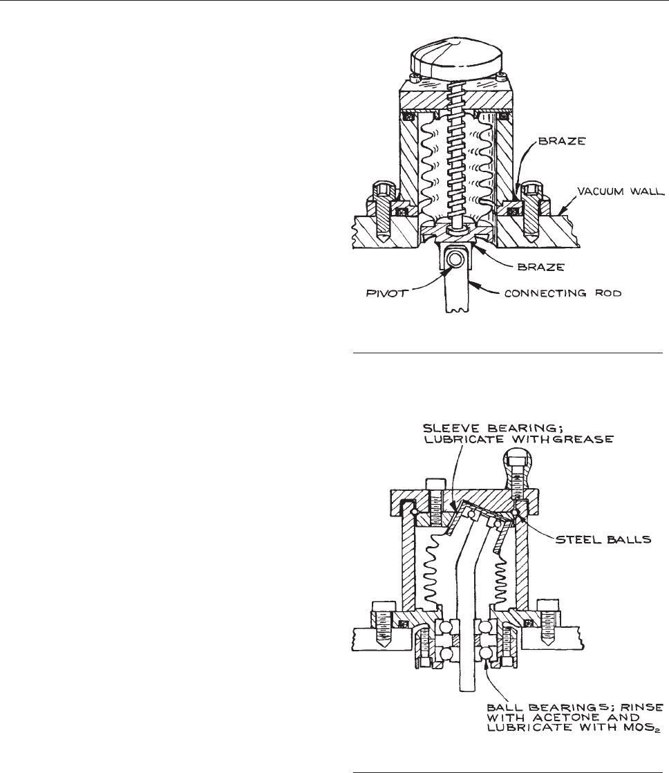
provide a more or less precise micrometer drive to control
the moving element. In general, a leak valve should never
be used to shut off the flow of gas, as deformation of one of
the two elements will result in a loss of low-flow control. A
shutoff valve, if required, should go on the upstream side
of a leak valve and as close to the inlet as possible to
minimize the ‘‘dead’’ volume of gas that must be pumped
through the leak valve. A sintered metal filter should
always be used at the inlet of a leak valve. The smallest
piece of solid material compressed against the seat of a
leak valve will certainly cause irreversible damage.
3.5.4 Mechanical Motion in the
Vacuum System
Mechanical motion can be transmitted through the vacuum
wall using a sliding seal, a flexible wall, or a magnetic
coupling.
Rotary motion at speeds up to 100 rpm may be trans-
mitted through an O-ring-sealed shaft. These seals are
inexpensive, but may fail if the O-ring becomes abraded.
In addition, lubricants and the elastomer O-ring material
are exposed to the vacuum.
A bellows seal to a shaft is the most common means to
permit motion to pass through the vacuum wall. A simple
and inexpensive linear-motion feedthrough can be made
from the actuator mechanism of a small bellows-sealed
vacuum valve. As shown in Figure 3.20, the valve body
is
truncated above the seat, a mounting flange is brazed to
the body, and a fixture is brazed or screwed to the valve
plate for attaching the mechanism to be driven inside the
vacuum. Rotary motion may be transmitted through a
bellows-sealed ‘‘wobble driv e,’’ illustrated in Figure 3.21.
Relati
vely inexpensive rotary drives of this type are avail-
able from most vacuum-hardware suppliers. Much more
expensive and more complex drives are also available,
including drives that provide three-axis rotation and
three-axis translation.
Moving parts can be magnetically coupled through a
vacuum wall. This scheme is particularly useful for the
transmission of linear motion through the wall of a glass
vacuum system. The driven element is attached to a block
of magnetic material such as iron or nickel that is placed
against the inside of the vacuum wall. A magnet can then
drag the driven element along the wall. A more exotic
Figure 3.20 A bellows-sealed valve [Figure 3.19(a)]
converted to a linear-motion feedthrough.
Figure 3.21 Bellows-sealed, wobble-drive, rotary-motion
feedthrough.
VACUUM HARDWARE 123

application of magnetic forces is found in the use of ferro-
magnetic fluids as shaft seals held in place by magnetic
fields. Ferrofluidic shaft seals rated for 5000 rpm at 10
9
torr are commercially available (A&N Super-Seal
TM
).
Metal surfaces become very clean in vacuo, particularly
after baking, and metals in close contact tend to cold-weld.
Because of this, unlubricated bearing surfaces within a
vacuum system often become very rough after only a little
use. Liquid lubricants can be used if they are thoroughly
outgassed before installation. The vapor pressure of the
lubricant will be the limiting factor. Diffusion pump oils
can be used in diffusion-pumped vacuum systems, since the
ultimate pressure is determined by the room-temperature
vapor pressure of the oil in the pump. Polyphenylether
oils lubricate well and are among the lowest-vapor-pressure
oils. Perfluorinated oils, such as DuPont Krytox 143AZ,
are an excellent choice for liquid lubrication in a vacuum.
A difficulty with liquid lubricants is their tendency to creep
out of a bearing and along the surface of a shaft. A creep
barrier can be placed between a lubricated bearing surface
and the surroundings. This may consist of a coating or a
plastic lip of a material such as Teflon that is not wetted by
the lubricant.
There are a number of methods of improving bearing
performance in a vacuum system without introducing
high-vapor-pressure oils into the vacuum. The tendency
for a bearing to gall is reduced if the two mating bearing
surfaces are made of different metals. For example, a steel
shaft rotating without lubrication in a brass or bronze journal
will hold up better than in a steel bushing. A solid lubricant
may be applied to one of the bearing surfaces. Silver, lead–
indium, and molybdenum disulfide have been used for this
purpose. Graphite does not lubricate in a vacuum; MoS
2
is
probably best. The lubricant should be burnished into the
bearing surface. The part to be lubricated is placed in a lathe.
As the part turns, the lubricant is applied and rubbed into the
surface with the rounded end of a hardwood stick. By this
means, the lubricant is forced into the pores. After burnish-
ing, the surface should be wiped free of loose lubricant.
One component of a bearing may be fabricated of a self-
lubricating material such as nylon, Delrin, T eflon, or poly-
imide. Teflon is good for this purpose, but its propensity to
cold-flow will cause the bearing to become sloppy with time.
Polyimide can be used in ultrahigh vacuum after baking to
250–300 ºC. Brown, Sowinski, and Pertel
6
have overcome
the cold-flow problem in the design of a dri v e screw for use
in a vacuum. Both the screw and its nut are steel, and lubri-
cation is accomplished by placing a Teflon ke y in a slot cut in
the side of the screw. Teflon is then continuously wiped onto
the screw threads as the screw turns.
For very precise location of rotating parts and for high
rotational speeds, ball bearings are required. Precision,
bakeable ball bearings can be fabricated using sapphire
balls running in a stainless-steel race. Inexpensive preci-
sion sapphire balls are available from Industrial Tectonics.
A ball retainer is required to prevent the balls from rubbing
against one another (see Section 1.7.3). Without grease or
oil lubrication, it is helpful to burnish the race with MoS
2
.
For high-speed applications a fluid lubricant is necessary.
The following process has been developed at NASA-
Goddard Space Flight Center:
7
purchase high-quality stain-
less-steel ball bearings with side shields and phenolic ball
retainers, such as the New Hampshire PPT series or Barden
SST3 series. Remove the shields and leach clean the phe-
nolic by boiling the bearings in chloroform – acetone, and
then vacuum-dry at 100 ºC. The bearings are then lubricated
by impregnating the phenolic with DuPont Krytox 143AZ, a
fluorinated hydrocarbon. Impregnation is accomplished by
immersing the bearing in the lubricant and heating to 100 ºC
at a pressure of 1 torr or less until air stops bubbling out of
the phenolic. After this process the bearing must be wiped
almost dry of lubricant. The Texwipe Company makes
ultraclean foam cubes for this process. The amount of lubri-
cant in the bearing is determined by weighing before and
after impregnation. About 25 mg of Krytox is required for
an R4 (1/4in.) bearing, and about 50 mg is needed for an R8
(1/2 in.) bearing. This lubrication process should be carried
out in a very clean environment, and the bearing should be
inspected under a microscope for cleanliness before the side
shields are replaced. Bearings treated in this manner have
been run at speeds up to 60 000 rpm in vacuo.
3.5.5 Traps and Baffles
Traps are used in vacuum systems to intercept condensable
vapors by means of chemisorption or physical condensa-
tion. When an oil-sealed mechanical pump is used as the
backing pump for a diffusion pump or a turbomolecular
pump, a trap is placed in the foreline between the backing
pump and the high vacuum pump to prevent backstreaming
124 VACUUM TECHNOLOGY
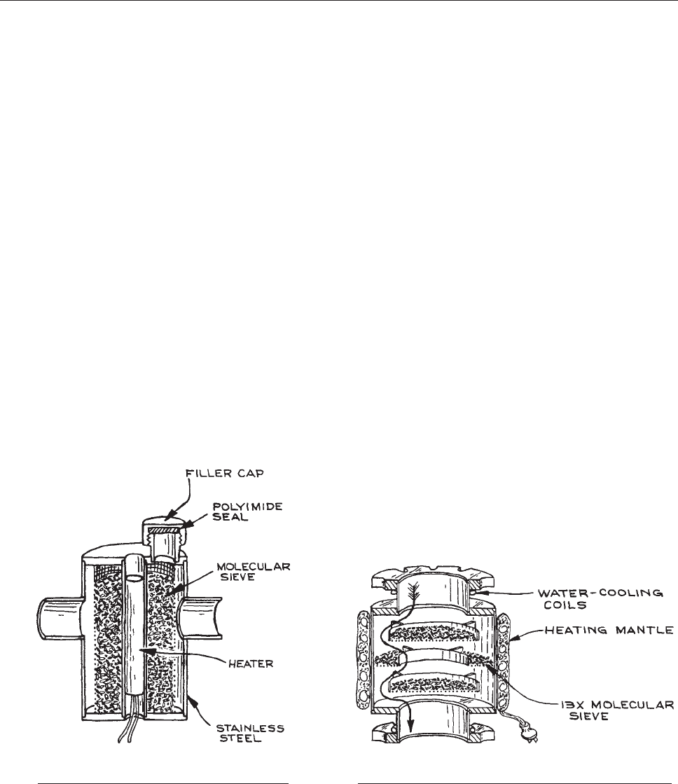
of mechanical pump oil vapor. This is absolutely essential
for the creation of a hydrocarbon-free vacuum. In some
applications, such as vacuum processes employed in the
semiconductor industry, the foreline trap is intended to
condense corrosive gases from the process chamber in
order to prevent harm to the forepump. In addition, a trap
is placed between a diffusion pump and a vacuum chamber
to pump water vapor and to remove diffusion-pump fluid
vapors that migrate backwards from the pump toward the
chamber.
In many foreline traps, an ultraporous artificial zeolite
known as molecular sieve is employed to adsorb oil vapor.
These traps are similar in design to the molecular-sieve
sorption pumps previously described, except, of course,
that a trap must have both an inlet and an outlet. A typical
foreline trap filled with zeolite 13X molecular sieve is
shown in Figure 3.22 . The molecular sieve is initially acti-
v
ated by baking to 300 ºC for several hours. In use the
sieve material is regenerated at intervals of about two
weeks by baking under vacuum to drive out adsorbed oil
and water. Care must be taken to prevent the oil driven out
of the trap from condensing upstream of the trap, thus
doing more harm than good. A valve on the upstream side
of the trap can be closed to prevent oil vapor from back-
streaming, provided that the valve and the connection to
the trap are themselves heated to prevent condensation
while the trap is being baked. It is also possible that vapor
driven from the trap will contaminate the forepump. Some
trap designs provide a third connection for a separate
pump to be used during the bakeout. Another trap design
provides a removable basket for the sieve charge that can
be baked in a separate oven. For a system that must be kept
in continuous operation, two traps in parallel are used.
Valves on each side of both traps allow one trap to be
isolated for regeneration. An auxiliary pump (with suitable
valving) is used to evacuate the trap being regenerated.
The lowest pressure attai nable with a two-stage oi l-
sealed mechanical pump is initially determined by the
vapor pressure of the o il in the pump. By using a molec-
ular-si eve tr ap in series with a mechanical pump to
remove oil vapor, it is possible to achieve p ressures as
low as 10
4
torr in a small system with no gas load. This
is an e ffective scheme for maintaining a vacuum for ther-
mal insulation.
Molecular sieve may also be used in a high-vacuum
trap over the inlet of an oil diffusion pump. As shown in
Figure 3.23, these traps are designed to be optically
opaque,
so that a molecule cannot pass through the trap
in a straight line. This precaution is necessary because this
type of trap is intended for use at pressures where the
mean free path of a molecule is very long. To ensure high
conductance, the inlet and outlet ports should have the
same cross-sectional area as the inlet of the attached pump.
Also, the cross-section perpendicular to the flow path
Figure 3.22 A foreline trap filled with
molecular sieve.
Figure 3.23 High-vacuum molecular-sieve trap for use over
the inlet of a diffusion pump.
VACUUM HARDWARE 125

through the trap (indicated by an arrow in Figure 3.23)
should be at least as large as that of the inlet and outlet
ports. The molecular sieve is activated by baking under
vacuum to 300 ºC for at least six hours. The trap may be
heated with heavily insulated heating tape or a custom-
made heating mantle such as those obtained from the
Glas-Col Apparatus Company. The flanges of the trap
are water-cooled to prevent overheating the seals.
The maintenance of a high-vacuum trap is different
from that of a foreline trap. A high-vacuum molecular-
sieve trap is placed above an oil diffusion pump, and a gate
valve is located above the trap to permit isolation of
the trap and pump stack from the vacuum chamber.
After the initial bakeout the pump is run continuously, so
that the trap is always under vacuum. The isolation valve is
closed whenever it is necessary to open the chamber to the
atmosphere, and the chamber is rough-pumped before
reopening the isolation valve. The molecular sieve cannot
be regenerated after the first bakeout. The initial bake of
the sieve results in the evolution of water vapor, but sub-
sequent baking would drive out absorbed pump-fluid
vapor. This oil vapor would condense on the bottom of
the isolation-valve gate and be exposed to the vacuum
when the valve is open. After the initial bakeout, the
molecular sieve will trap oil vapor effectively for a period
of several months if it is not exposed to moist air during
that period. When the sieve becomes clogged with
absorbed vapor, the base pressure of the pump-and-trap
combination will begin to rise. At this time the molecu-
lar-sieve charge should be replaced. If it is absolutely nec-
essary to stop the diffusion pump, the pump and trap
should be filled with argon or dry nitrogen and isolated
from the atmosphere in order to preserve the molecular
sieve.
Condensation traps employing cold surfaces – cold
traps – are used as foreline traps as well as inlet traps over
diffusion pumps. The coolant may be simply a flow of cold
water, an actively cooled refrigerant (Freon), or liquid
nitrogen. In principal, a trap cooled to liquid nitrogen
temperature would seem most effective, however, the
vapor pressure of most pump fluids is below 10
12
torr
at 40 ºC, a temperature easily achieved with a Freon
refrigerator.
A simple ‘‘thimble’’ trap is shown in Figure 3.24. These
trap
s are used as foreline traps or over a small diffusion
pump. For periodic operation, the thimble can be filled with
liquid nitrogen. The coolant must be replenished every few
hours. For continuous, long-term operation, an alternative,
shown in the figure, is to fill the trap with a low-melting
liquid, such as isopropyl alcohol, and refrigerate the liquid
with an immersion cooler (Neslab Instruments; FTS
Systems). These coolers consist of a refrigerator housed in
a small console, with a hose to carry refrigerant to a flexible
probe that is inserted in the bath in the trap. A temperature
of 40 ºC is easily attained with the smallest unit since the
only heat load is thermal leakage from the surroundings into
the trap. A liquid-nitrogen-cooled cryotrap for use over a
large diffusion pump is illustrated in Figure 3.25. These
tr
aps are connected to a large liquid-nitrogen Dewar with
a valve operated by a sensor that detects the coolant level in
the trap. When a cold trap is permitted to warm up, it must
be isolated from the vacuum chamber so that condensed
material does not migrate into the chamber. Also the trap
should be vented so that the evaporating condensate does
not build up a dangerously high pressure.
Figure 3.24 A thimble trap cooled by the flexible, cooled
probe of an immersion cooler.
126 VACUUM TECHNOLOGY
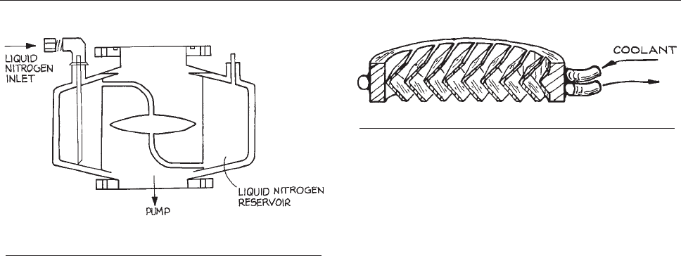
An optically dense ‘‘chevron’’ baffle of the type shown
in Figure 3.26 is usually placed over the inlet of a diffusion
pump.
These baffles may be air-cooled, water-cooled, or
cooled by refrigerant from a small refrigerator. Recently,
baffles with thermoelectric coolers operating at 35 ºC
have become available. In addition to reducing back-
streaming of pump-fluid vapor, a baffle serves as a radia-
tion barrier between the hot pump and the cold trap or
vacuum system above the baffle.
3.5.6 Molecular Beams and Gas Jets
Often it is necessary to introduce a gaseous sample into a
vacuum system. The sample may be contained in a small
chamber with holes suitably located to admit probes such
as light beams or electron beams; however, the walls of
such a chamber may prove a hindrance to the proposed
experiment. Alternatively, a gas can be introduced as an
uncontained, but directed, beam of atoms or molecules.
The absence of walls is only one of the advantages to using
a gas beam. Because of the directed velocities of the par-
ticles in the beam, it is possible to maintain the sample in a
collisionless environment while still obtaining useful den-
sities. The beam can be crossed with another beam or
directed at a surface to obtain collisions of a specified
orientation. Under appropriate conditions, the expansion
of a jet of gas results in extreme cooling to give a very
narrow population distribution among quantum states of
molecules in the gas. Lucas succinctly stated the case for
atomic or molecular beams when he observed that ‘‘beams
are employed in experiments where collisions ...are
either to be studied, or to be avoided.’’
8
Permitting gas to flow into a vacuum through a tube
creates a gas beam. The nature of the beam depends upon
whether the flow exiting the tube is in the molecular- or the
viscous-flow regime. Apertures placed downstream of the
channel through which the gas flows into the vacuum can
establish the shape of the beam.
We begin with the molecular-flow case, where the mean
free path, k, at the outlet of the gas channel is greater than
the diameter d of the channel. For the case of flow from a
region of relatively high pressure into a vacuum through a
round aperture (that is, a tube of length l ¼ 0), the flux
distribution in the direction specified by the angle h rela-
tive to the normal to the aperture surface is:
I hðÞ¼I h ¼ 0ðÞcos h ðatoms s
1
sr
1
Þð3:27Þ
The beam width H specified as the full angular width meas-
ured at the angle where the flux has fallen by half is 120º.
Increasing the length l of the tube or channel through which
the gas flows into the vacuum can narrow the beam. Any
description of the gas beam issuing from such a channel must
consider the molecular diameter and the nature of the scatter-
ing of molecules from the walls of the tube. Both theoretical
and experimental inv estigations have been carried out in an
effort to describe a gas beam in terms of easily measured
parameters. In comparing experiment and theory it has turned
out that the observed flux and the sharpness of the beam fall
short of theoretical expectations by a factor of two to fiv e.
In general, both experimental and theoretical results imply
that to obtain useful fluxes and reasonable collimation, a
beam source consisting of a tube or channel must be at least
10 times greater in length than its diameter, and the gas
pressure behind this channel should be such that d < k < l.
Lucas has devised a succinct description of gas beams in
the molecular-flow regime in terms of a set of reduced
parameters.
8
The gas pressure P behind the channel (in
Figure 3.25 Liquid-nitrogen-cooled cryotrap for a diffusion
pump.
Figure 3.26 Cooled baffle.
VACUUM HARDWARE 127

torr), the beam width H (degrees), and the gas particle flux
I [atoms s
1
sr
1
(on axis)] and throughput q (atoms s
1
)
are related to the corresponding reduced parameters by:
P ¼
P
R
lr
2
H ¼
H
R
d
l
I ¼
T
295M
1=2
d
2
I
R
lr
2
q ¼
T
295M
1=2
d
3
q
R
l
2
r
2
ð3:28Þ
where T is the absolute temperature, M is the molecular
weight, d and l are in cm, and r is the molecular diameter
in A
˚
(10
8
cm). For pressures roughly in the range where
d < k < l, the reduced half angle, flux, and throughput
are related to the reduced pressure by:
H
R
¼ 2:48 3 10
2
ffiffiffiffiffiffi
P
R
p
I
R
¼ 1:69 3 10
20
ffiffiffiffiffiffi
P
R
p
q
R
¼ 2:16 3 10
21
P
R
ð3:29Þ
From model calculations, Lucas found that to obtain max-
imum intensity for a given angular width H, the reduced
pressure P
R
should not be less than unity.
For design work, a useful ‘‘optimum’’ equation can be
derived by combining the above and setting P
R
¼1 to give:
I ¼ 6:7 3 10
17
T
295M
1=2
dH
r
2
ð3:30Þ
the optimum axial intensity for a given channel diameter and
desired angular width. The tube length is fixed by the equa-
tions for H and H
R
(P
R
¼ 1) above, and the input pressure
by the equation for P. Operating at somewhat higher pres-
sures gives some control over the flux and throughput with-
out significantly departing from the optimum condition.
The construction of low-pressure, single-channel gas-
beam sources is fairly straightforward. An excellent source
can be made of a hypodermic needle cut to the appropriate
length. These needles are made of stainless steel, they are
av ailable in a wide range of lengths and di ameters, and they
come with a mounting fixture that is reasonably gas tight.
The goal of high intensity in a sharp beam is incompat-
ible with a single-channel source because, for a given
beam width, the gas load (throughput) increases more
rapidly than the flux as the channel diameter is increased.
The solution to this problem is to use an array of many
tubes, each having a small aspect ratio (i.e., d/l << 1).
9
Tubes with diameters as small as 2 3 10
4
cm and lengths
of 1 3 10
1
cm arranged in an array a centimeter or more
across are commercially available in glass (Burle Electro-
Optics, Pegasus Glassworks, Hamamatsu).
When the gas pressure behind an aperture or nozzle
leading to a vacuum is increased to the extent that the mean
free path is much smaller than the dimensions of the aper-
ture, a whole new situation arises. Not only is the density
of the resultant gas jet much greater than in the molecular-
flow case, but also the shape of the jet changes and the gas
becomes remarkably cold. This is a direct result of colli-
sions between molecules in the gas as it expands from
the orifice into the vacuum. Because of collisions, the
velocities of individual molecules tend toward that
of the bulk gas flow, just as an individual in a crowd
tends t o be dragged along with the crowd. The transla-
tional temperature of the gas, defined by the width of its
velocity distribution, decreases, while the bulk-flow
velocity increases. The c onversion of random molecular
motion into directed motion continues until the gas
becomes too greatly rarefied by expansion, at which point
the final temperature is frozen in. Because the mass-flow
velocity increases while the local speed of sound, propor-
tional to the sq uare root of the translational temperatur e,
decreases, the Mach number rise s and the flow becomes
supersonic. Inelastic molecu lar collisions in the expand-
ing gas also cause internal molecular e nergy to flow into
the kinetic energy of bulk flow, with the result that there
may be substantial rotational and vibrational relaxation.
Rotational tempe ratures less than 1 K and vibrational
temperatures less than 50 K have been obtained. At these
low temperature s only a small number of qua nt um states
are occupied, an ideal c ondition for a variety of spectro-
scopic studies.
The low temperatures obtained in a supersonic jet can
present some problems. Chief among these is that of
condensation. Collisions in the high-density region of the
jet cause dimer or even polymer formation. With high-
boiling samples, bulk condensation may occur. Of course,
128 VACUUM TECHNOLOGY

if one wishes to study dimers or clusters, this condensation
is desirable. To avoid dimer formation, the sample gas is
mixed at low concentration with helium. This seeded gas
sample is then expanded in a jet. Adjusting its concentra-
tion in the helium carrier controls the degree of clustering
of the seed-gas molecules.
The cooling effect, as well as the directionality of the
jet, is lost if the expanding gas encounters a significant
pressure of background gas in the vacuum chamber.
Unfortunately, optimum operating conditions require a
large throughput of gas into the chamber. The extent of
cooling depends upon the probability of binary collisions,
which is proportional to the product P
0
d of the pressure
behind the nozzle and the diameter of the nozzle. Further-
more, to minimize condensation, the ratio d/P
0
should be
as large as possible. The result, in practice, is that a large-
capacity vacuum pumping system is needed. In typical
continuously operating supersonic-jet apparatus, source
pressures of 10 to 100 atm have been used with nozzle
diameters of 0.01 cm down to 0.0025 cm. The conductance
of an aperture under these conditions is roughly:
C ¼ 15 d
2
Ls
1
ð3:31Þ
when the diameter is in centimeters. This implies a
throughput on the order of 10 torr L s
1
. To obtain a mean
free path of several tens of centimeters, a base pressure of
about 10
4
torr is required. A pump speed approaching
10 000 L s
1
may be necessary. Typically, several large
diffusion pumps are used. When possible the jet is aimed
straight down the throat of a pump.
In many experiments the cold molecules in a supersonic
jet are only probed periodically – as, for example, when
doing laser spectroscopy with a pulsed laser. Operation of
the jet in a synchronously pulsed mode can reduce the gas
load on the pump by several orders of magnitude compared
to that in the continuous mode. A number of fast valves for
this purpose have been devised.
10
The simplest are based
upon inexpensive automobile fuel injector valves.
11
Gen-
eral Valve produces a system consisting of a pulsed valve
and driver that operates at pulse rates as high as 250 Hz
with a pulse width as small as 160 ls.
Another efficient means of dealing with the background-
gas problem has been demonstrated.
12
This relies upon the
fact that interaction of the expanding gas with the back-
ground gas gives rise to a shock wave surrounding the gas
jet. If the pressure P
0
behind the nozzle is increased, it is
possible to achieve a mode of operation where a rarefied
region is created behind the shock wave. In the region
upstream of the shock front, the gas behaves like a free
jet expanding into a perfect vacuum. The distance from the
nozzle to the shock front is:
‘ ¼ 0:67d
P
0
P
1=2
ð3:32Þ
where P
0
is the pressure in the nozzle, P the background
pressure, and d the nozzle diameter. When the nozzle pres-
sure is sufficiently high to achieve a free jet length of
usable dimensions, the background pressure will increase
greatly. This state of affairs has a distinct advantage, since
at a high background pressure, a large throughput can be
achieved with a pump of moderate speed. For example, to
obtain a free length ‘ ¼ 1 cm with a 0.01 cm nozzle and a
source pressure of 10 atm, the background pressure should
be about 400 mtorr. The throughput in this case is about
10 torr L s
1
and the required pumping speed, 25 L s
1
,
could be achieved by a large rotary mechanical pump or a
Roots pump of modest capacity.
The fabrication of a nozzle is straightforward, although
some difficulty may be encountered in making the neces-
sary small hole. A skillful mechanical technician can drill
a hole as small as 0.01 cm diameter. Smaller holes can be
made by spark or electrolytic erosion, or by swaging a hole
closed on a piece of hard wire and then withdrawing the
wire. One of the first small, high-pressure nozzles
12
was
made by drilling down the axis of a stainless-steel rod to
within 0.1 mm of the end with a drill bit having a sharp
conical point. A 0.0025 cm diameter hole was then made
through the remaining metal by spark erosion.
For many experiments, the gas flowing into a vacuum
system through an aperture or a channel produces a beam
that is too broad or too divergent for the intended applica-
tion. In this case one or more apertures placed downstream
from the source can define the beam shape. Often it is
advantageous to build these apertures into partitions that
separate the vacuum housing into a succession of cham-
bers. Each chamber can be evacuated with a separate
pump. The pressure in the first will be highest, so that
the large throughput obtained here will significantly reduce
VACUUM HARDWARE 129

the gas load on the next pump. This scheme is called differ-
ential pumping (see Section 3.6.2).
An
aperture downstream of a supersonic jet, but close
enough to be in the viscous-flow region, is called a skimmer.
The design of these skimmers is critical, since they tend to
produce turbulence that will destroy the directionality of
the flowing gas. A skimmer is usually a cone with its tip cut
off and the truncated edge ground to knife sharpness. The
details of the design, location, and fabrication of a skimmer
are beyond the scope of this book, and the interested reader
should refer to a specialized text on this subject.
13
3.5.7 Electronics and Electricity in Vacuo
At low frequencies the vacuum between electrodes or wires
provides excellent insulation. At pressures below 10
4
torr,
the breakdown voltage between smooth, gently rounded
surfaces is in excess of 1000 V for each millimeter of
separation. Occasionally sparking will occur between
newly made parts because of high field gradients around
whiskers of metal. These whiskers quickly evaporate and
sparks do not recur. The challenge in making electrical
devices function in vacuum is in the design of spacers
and other elements that locate electrodes and wires that
are at different electrical potentials. Insulating materials
must possess adequate mechanical strength and be compat-
ible with the vacuum environment and available fabrication
processes. In addition, insulators must be very clean. Elec-
trical breakdown in the vacuum is usually initiated by a
discharge traveling along the surface of an insulator.
Ceramic materials are the best insulators and, among
these, alumina (at least 96% Al
2
O
3
) is probably the best.
Simple shapes such as rods, tubes, and balls are readily
available to be incorporated in insulator asse mblies (see
Figures 5.40 and 5.41). More complex shapes require spe-
cia
lized grinding techniques. Alumina circuit board
substrate is available as plate .010 in. to .060 in. thick
and 6 in. square. Owing to the scale of the circuit-board
industry, the faci lities for custom fabrication by laser cut-
ting of alumina plate are widely available. The d esigner of
vacuum apparatus can n ow spe cify quite complex shapes
cut from al umina plate at a cost of just a few dollars a
piece. A simple scheme employing alumina washers to
locate and insulate electrically isolated parts is illustrated
in Figure 3.27(c).
Alumina
can be metalized and subsequently joined by
brazing to stainless steel or Kovar structures. It is imprac-
tical to attempt this process in the lab; however, this
technology is employed in many standard vacuum compo-
nents, such as electrical feedthroughs (Ceramseal, Insula-
tor Seal) to be inserted in the vacuum wall [Figure 3.27(d)]
and
ceramic ‘‘breaks’’ built into the middle of a length of
metal vacuum tubing [Figure 3.27(e)].
A
few precautions should be observed in designing and
mounting ceramic parts. Ceramic materials are strongest in
compression and cannot be plastically deformed. The best
design of an assembly with ceramic components captures
each ceramic part between smooth surfaces that are
aligned with the face of the part so that shear forces are
not applied to the ceramic material.
Ceramics are often used simultaneously for electrical
insulation and thermal isolation. In this case it is impor-
tant to be aware of the strong dependence of electrical
resistivity on temperature. The resistivity of a ceramic
material falls by roughly a factor of 10 for every 100 ºC
increase in temperature.
14
For example, the resistivity of
alumina is greater than 10
17
ohm cm at 100 ºC and falls
below 10
7
ohmcmat1000ºC.
The surface of a ceramic part is more or less porous
and susceptible to trapping contaminates. In handling
ceramic parts, inorganic salts from skin oils may be
transferred fr om the fingers to the surface of the ceramic.
Salts absorb water a nd encourage electrica l conduction
across the surface. A part should be c leaned with organic
solvents to remove oils followed by a final rinsing in hot
distilled water to remove these salts. Rinsing with pure
methanol and heating can dry the part. Surgical gloves
should be worn to handle a part after it has been cleaned.
If the spacing between wires in a vacuum system cannot
be reliably maintained, then insulation is required. Ordinary
Teflon-insulated, solid, hookup wire may be used down to
10
7
torr, although air bleeding out from under the insu-
lation will slow pumpdown. Stranded wire should never be
used, as gas is trapped between the strands. At very low
pressures and high temperatures, wires can be insulated by
stringing ceramic ‘‘fish spine’’ beads (from Coors) [Figure
3.27(a)] or pieces of Pyrex tubing over them. The spacing
between
wires can be maintained with ceramic wire looms
[Figure 3.27(b)] available from many suppliers of vacuum
apparatus.
Wire insulated with a Kapton (polyimide) film
130 VACUUM TECHNOLOGY
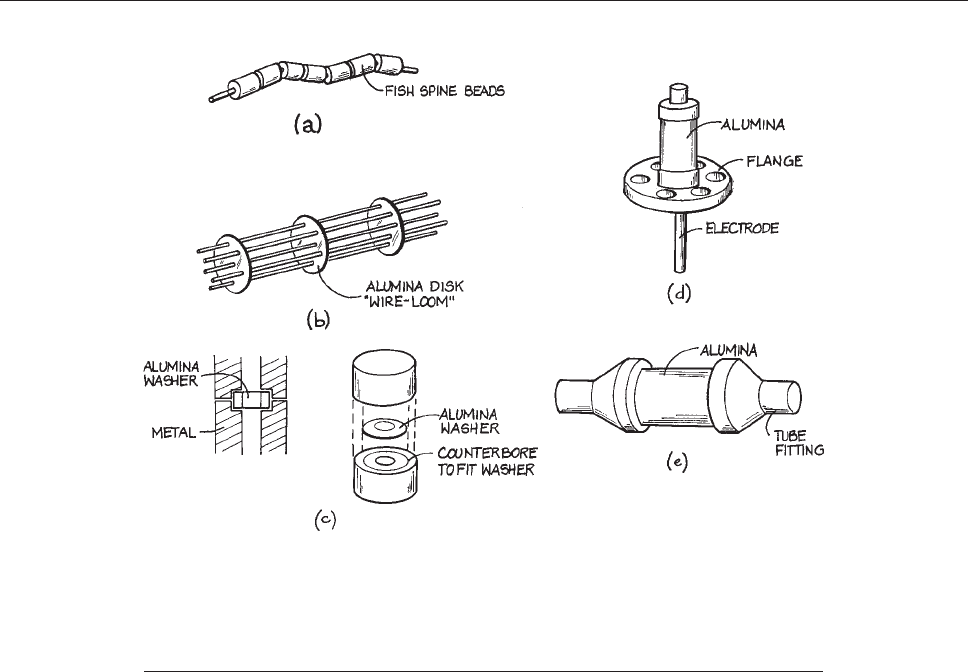
or a ceramic coating is available from vacuum-equipment
suppliers for use in UHV. The latter is better for use at
elevated temperatures, but has the disadvantage of shed-
ding bits of ceramic material when flexed. Electrical solder
should not be used for electrical connections in a vacuum
system because the lead in solder and soldering flux con-
taminate the vacuum. Mechanical connections are prefera-
ble. Wrapping a wire under the head of a screw and
tightening the screw can make connections to electrodes.
Wires may be jointed by slipping the ends into a close-
fitting piece of tubing and crimping the tubing onto the wire.
A variety of wire connectors are available from vacuum-
equipment suppliers. Tungsten, molybdenum, nichrome, or
stainless-steel wires may be spot-welded together. In weld-
ing refractory metals, a more secure weld is obtained if a
piece of nickel foil is interposed between the wires.
Electronic devices tend to overheat in a vacuum since
the only cooling is by radiation. Electronic components
such as power transistors and integrated circuits that must
dissipate more than about 2 watt are particularly unreliable.
Such devices can be placed in vacuum-tight, gas-filled
boxes that are thermally connected to the vacuum wall.
Electrical feedthroughs for wires passing through the wall
of a glass vacuum system are illustrated in Figure 3.28.As
de
scribed in Section 2.3.10, an electrical feedthrough can be
ma
de by sealing a tungsten rod directly into a hard glass
wall. An easier solution is to braze an electrode into the
metallic end of a standard Kovar-to-glass graded seal and
join the glass end of the seal to the glass vacuum wall.
3.6 VACUUM-SYSTEM DESIGN
AND CONSTRUCTION
Before beginning the design of a vacuum system, a number
of parameters must be specified in at least a semiquantitati v e
Figure 3.27 Applications of ceramics for electrical insulation in vacuum systems: (a) ceramic
‘‘fish spine’’ beads threaded on a wir e as insulation; (b) ceramic disk with holes used as a
wire-loom to keep wires in a bundle from touching one another; (c) design for electrodes
located and electrically isolated with spacers laser-cut from alumina circuit-board substrate;
(d) a ceramic-insulated electrical feedthrough; (e) a ceramic break in a vacuum line
mounted between two standard vacuum flanges.
VACUUM-SYSTEM DESIGN 131

manner. The size and shape of the vacuum chamber must
be determined. The desired ultimate pressure and the com-
position of the residual gas in the chamber must be speci-
fied. One must estimate the gas load on the pumps. The
amount of money and time available are also important
considerations. It is instructive to spend a few evenings
leafing through vacuum-equipment manufacturers’ cata-
logs to become familiar with the specifications and cost
of commercial vacuum components. The author has found
the Kurt J. Lesker, Co., Leybold AG, and Varian Vacuum
catalogs to be especially informative.
The ultimate pressure requirement dictates the choice of
the primary pump. Cost and limitations on hydrocarbon
contamination will determine the choice of roughing and
backing pumps. An ultimate pressure down to about 1 mtorr
can be achiev ed with a mechanical pump with an appropriate
trap. Sorption pumps can be used on a system requiring an
ultimate pressure of 1 mtorr if there is not a large continuous
gas load. Ultimate pressures in the high-vacuum range do wn
to about 10
9
torr can be achieved with a diffusion pump, a
turbomolecular pump, or a cryopump. True ultrahigh-
va cuum systems ordinarily use ion pumps and titanium sub-
limation pumps. Ultrahigh vacuum can also be achiev ed with
turbomolecular pumps. To reach UHV starting from a back-
ing pressure near 1 torr requires a compression ratio
approaching 10
12
. This can be accomplished with two turbo-
molecular pumps operating in series, a turbo backed with a
drag pump, or with a compound turbomolecular/drag pump.
The cost of a vacuum system is about equally divided
between the cost of the pumps and the cost of the v acuum
vessel and ancillary hardware, such as gauges and valves. In
terms of cost per unit pumping speed, mechanical pumps are
most expensive – on the order of $100 per L/s. Most systems
require a mechanical pump as either the primary pump or a
backing pump; howe ver, since they operate at relativ ely high
pressures and correspondingly high throughputs, one ordina-
rily finds that for laboratory apparatus only modest pumping
speed is required of a mechanical pump – a few L/s to a fe w
tens of L/s. For high-vacuum systems, diffusion pumps are
most cost effecti ve although sorption or cold traps needed to
prev ent hydrocarbon contamination will add to the total cost.
The cost of a diffusion pump amounts to $2 to $5 per L/s of
pumping speed. A turbomolecular pump with its controller, a
cryopump with a refrigerator, or an ion pump and controller
will cost five to ten times as much as a diffusion pump of
comparable pumping speed.
There are three sources of gas that must be pumped out
of a vacuum vessel: molecules adsorbed on the walls of the
container, as well as the components therein, gas intention-
ally admitted as part of the process under study, and leaks.
The rate of outgassing of adsorbed water, carbon dioxide,
and hydrocarbons, and, ultimately, hydrogen, from the
surface of materials is difficult to measure. A summary
of published data is given in O’Hanlon’s book.
15
With care
in the choice and processing of the materials of construc-
tion of vacuum apparatus, it is generally possible to reduce
outgassing rates below 10
9
torr L s
1
cm
2
; lower yet
with baking. Similarly, actual leaks can be eliminated by
careful design and construction; so-called virtual leaks are,
however, more or less of a problem in all systems. Virtual
leaks are the result of gas being tapped in small occlusions
within the vacuum vessel. These typically occur where
parts are fitted together. Gas will be trapped between mated
surfaces and the conductance through the space between
such surfaces will be very small. The trapped gas may take
weeks to be pumped away and thus acts as a continual gas
load on the pump. Every effort should be made to vent
these spaces with pumpout holes (Figure 3.40).
3.6.1 Some Typical Vacuum Systems
Diffusion-Pumped System. A diffusion-pumped
vacuum system is shown schematically in Figure 3.29.
Figure 3.28 Electrical feedthroughs in a glass vacuum wall
employing (a) a tungsten-to-metal seal; (b) a standard
Kovar-to-glass seal.
132 VACUUM TECHNOLOGY
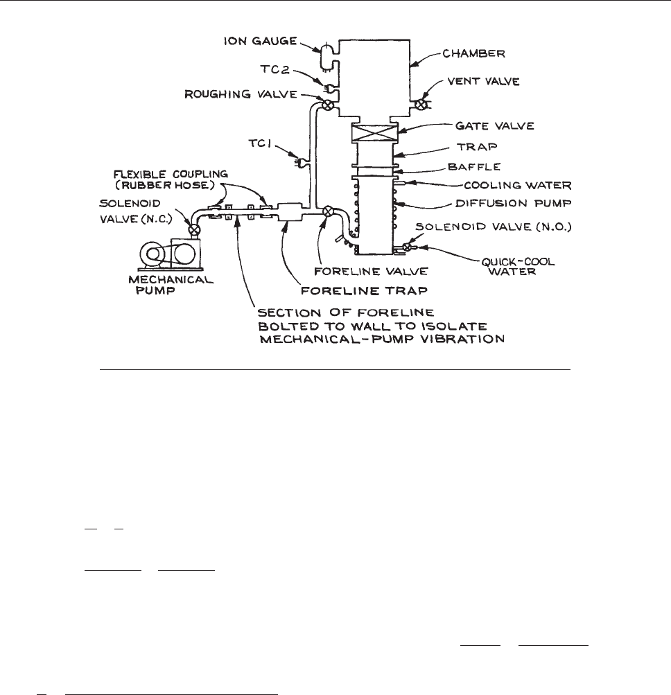
For illustration, suppose the vacuum chamber is constructed
of stainless steel and is 30 cm in diameter and 30 cm high
with a surface area of 5000 cm
2
. If the pump stack consists
of a 2 in. oil diffusion pump with a speed of 150 L s
1
, and
a trap and baffle with a conductance of 200 L s
1
, the net
speed of the pump stack will be:
S ¼
1
S
p
þ
1
C
1
¼
1
150 L s
1
þ
1
200 L s
1
1
¼ 85 L s
1
ð3:33Þ
Assuming an initial outgassing rate of 10
9
torr L s
1
cm
2
,
the vacuum vessel will pump down to:
P ¼
Q
S
¼
5000 cm
2
3 10
8
torr L s
1
cm
2
85 L s
1
¼ 6310
7
torr ð3:34Þ
within a few hours. After a day of pumping and perhaps a
light bake to 100 ºC, the outgassing rate should fall below
10
9
torr L s
1
cm
2
and an ultimate pressure in the 10
8
torr range should be achievable.
The size of the backing pump is determined from
the maximum throughput of the diffusion pump. This
occurs after the vacuum vessel is rough pumped and the
gate valve over the diffusion pump is first opened. The
pressure in the vessel at this time should not be greater than
about 50 mtorr. The maximum throughput will then be:
Q
max
¼ P
max
S ¼ 5 3 10
2
torr
3 85 L s
1
¼ 4 torr L s
1
ð3:35Þ
The foreline pressure must always remain below about 200
mtorr so the speed of the backing pump should be:
S
p,backing
¼
Q
max
P
backing
¼
4 torr L s
1
2310
1
torr
¼ 20 L s
1
: ð3:36Þ
A small two-stage mechanical pump can meet this
requirement.
The conductance of the foreline should be at least twice
the speed of the forepump so that the forepump is not
strangled by the foreline. To achieve a conductance of
Figure 3.29 Schematic diagram of diffusion-pumped high-vacuum system.
VACUUM-SYSTEM DESIGN 133

40 L s
1
at a pressure of 200 mtorr in a foreline a half
meter long, the diameter (from Section 3.2.4) must be:
D ¼
CL
180P
1=4
cm ðL in cmÞ
¼
40 3 50
180 3 2 3 10
1
1=4
¼ 2:7cm ð3:37Þ
In this case l in. copper water pipe would make an excel-
lent foreline.
To activate a system of the type shown in Figure 3.29,
starting
with all valves closed and the pumps off, proceed
as follows:
(1) Turn on the mechanical pump.
(2) When the pressure indicated by thermocouple gauge
1 (TC1) is below 200 mtorr, open the foreline valve.
(3) When TC1 again indicates a pressure below 200 mtorr,
turn on the cooling water and activate the diffusion
pump. The pump will require about 20 minutes to
reach operating temperature. When operating it makes
a crackling sound.
(4) Before pumping on the chamber with the diffusion
pump, the pressure in the chamber must be reduced to
a rough vacuum. Close the foreline valve and op en
the roughing valve. When the pressure indicated by
TC2 is below 50 mtorr, close the roughing valve and
open the foreline valve. The diffusion pump should
not be operated for more than two minutes with the
foreline valve closed. If necessary, interrupt the
roughing procedure, c lose the roughing valve, wait
for TC1 to indicate less than 200 mtorr, and reopen
the foreline valve for a moment to ensure that the
diffusion-pump outlet pressure does not rise above
about 200 mtorr.
(5) Slowly open the gate valve that isolates the diffusion
pump from the chamber. In less than 10 s the pressure
indicated by TC2 should fall below 1 millitorr and the
ionization gauge can be turned on.
A diffusion-pumped system of the type shown in Figure
3.29 is one of the most convenient and least expensive
systems
for obtaining high or even ultrahigh vacuum.
The system can be fabricated of metal or glass. A baffled,
but untrapped, oil diffusion pump on this system should
result in an ultimate pressure slightly below 10
6
torr.
With a cold trap an ultimate pressure of 10
9
torr is pos-
sible if the vacuum chamber is baked and only low-vapor-
pressure materials are exposed to the vacuum.
A number of inexpensive safeguards are incorporated
in the design in Figure 3.29 to avoid contamination or
damage
in the event of a loss of electrical power. A nor-
mally open (N.O.) sole noid-operated water valve in par-
allel with the pump heater admits water to the diffusion
pump, quick-cooling coils if the power fails. The diffu-
sion pump is isolated from the mechanical pump by a
nor mally closed (N.C. ) s olenoid valve to prevent air or
oil from being sucked through the mechanical pump into
the foreline. Special mechanical pump inlet valves are
available for this purpose (HPS Vacuum SentryÒ and
Leybold SECUVACÒ). These valves close automatically
when power is lost and vent the pump to atmosphere;
when power is reg ained, the valve does not reopen until
the pressure o n th e pu mp side falls to a few hundred
millitorr. The SECUVAC valve is also designed to c lose
in the even t of a sudden rise in inlet pressure. It is helpful
to place a ballast volume in the foreline to m aintain a
low foreline pressure while the diffusion pump cools
after a power outage. A relatively large foreline trap will
also serve as a ballast. A ballast tank of 5 to 10 L in the
foreline will permit the continued operation of the dif-
fusion pump for a period of perhaps 10 to 20 minutes
if the backing pump is turned off and the valve at the
inlet to the backing pump is closed. This intermittent
mode of operation can be useful in the event that vibra-
tion of the mechanical pump ha s an adverse effect on an
instrument housed in the h igh-vacuum chamber. For
example, this mode of opera tion is used on some electron
microscopes.
A useful fail-safe mechanism, not shown in Figure
3.
29, would be a water-pressure sensor in the water line
to
interrupt the electrical power if the water fails. Alter-
natively, a heavy-duty, normally closed (N.C.), bimetal-
lic temperature switch wired in series with the diffusion
pump heater may be mounted to the bottom turn of the
water-cooling coil. Then if the cooling-water flow is
inadequate, the rising temperature of the pump barrel
will interrupt the electricity to the pump heater. Many
diffusion pumps are equipped with a mounting plate for a
temperature switch that can be obtained from the pump
manufacturer.
134 VACUUM TECHNOLOGY
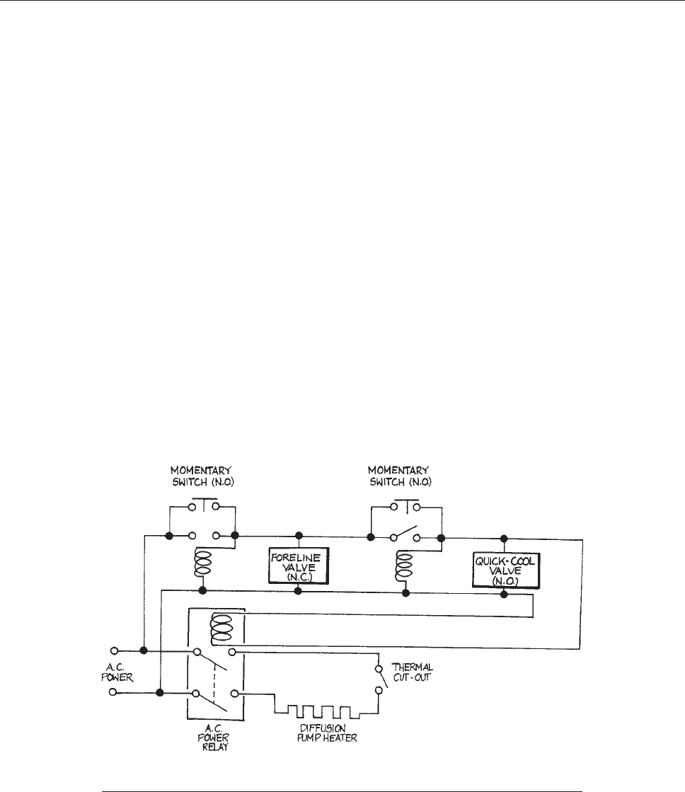
A power interruption in the operator’s absence threatens
serious contamination of the vacuum vessel, both at the
time the power goes off and when it comes back on again.
When the power goes off it is essential that the diffusion
pump stops operating before the foreline pressure rises
above the critical backing pressure. This is the purpose
of the quick-cool water valve described above. When
power is restored in the operator’s absence there is no
provision to rough out the vacuum vessel or otherwise
follow the orderly initiation of pumping described above.
As a minimum safeguard against a power failure, the
power to the system’s components should be supplied
through power relays that are wired to latch ‘‘off’’ until
reactivated by the operator. A latching relay circuit is
shown in Figure 3.30.
F
or a vacuum system that operates for long periods of
time without close supervision, it is worthwhile incorpo-
rating a control system that monitors the pressure in the
chamber and the foreline. Many high-quality commercial
thermocouple-gauge and ionization-gauge controllers
include relays that can be set to trip at a predetermined
pressure. The relay controlled by the foreline thermo-
couplegauge(TC1)canbesettotripat200–300mtorr.
This relay can be wired to operate a second, heavy-duty
relay that removes power from the diffusion pump and
simultaneously opens the quick-cool water valve and
closes the foreline sole noid valve at the mechanical
pump. The overpressure relay controlled by the ion
gauge can be employ ed to isolate the high-vacuum c ham-
ber by means of an electrically controlled, pneumatically
activated gate valve when the pressure in the chamber
rises above a few millitorr. In lieu of a gauge controller
with control relays, there are now available inexpensive,
modular, Pirani vacuum sensors with built-in pressure
switches (for example, the HPS Moducell). These can be
set to trip in the range 5 3 10
3
to 30 torr, making them
suitable for monitoring either the high-vacuum chamber or
the foreline. The design of a logical interlock system
employing temperature and pressure sensors to protect a
vacuum system is discussed in Sections 6.6.9 and 6.6.10.
A Small, Inexpensive Ultrahigh-Vacuum
System.
A small, inexpensive system, capable of
producing a vacuum of about 10
10
torr in a 1 L volume,
is illustrated in Figure 3.31. The entire system can be made
of
Pyrex. Constrictions in the glass tubing joining
Figure. 3.30 Relay circuit to latch ‘‘off’’ a diffusion-pumped vacuum system in the event of
a power failure.
VACUUM-SYSTEM DESIGN 135
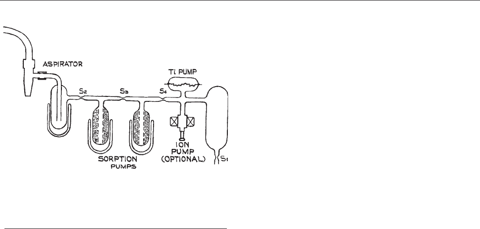
components of the system are fused closed with a
glassblower’s torch to seal off each part of the system as
evacuation proceeds. Rough pumping is initiated with a
water aspirator or alternatively a compressed-air Venturi
pump. High vacuum is achiev ed with sorption pumps
operated in sequence and ultrahigh vacuum is reached with
a titanium sublimation pump, possibly with the aid of a
small ion pump.
16
To achieve UHV, special precautions
are taken to displace rare gases from the system and to
remove water and carbon dioxide adsorbed on the walls of
the system. Neither sorption pumping nor gettering
effi ciently pumps rare gases, helium in particular. The rare
gases are swept from the system by a flow of dry nitrogen
before ev acuation is begun. The entire system is maintained
at a moderately high temperature throughout the entire
pumpdown procedure in order to driv e adsorbed gases off
the walls and into the pumps.
The pumpdown procedure for this vacuum system is as
follows:
(1) Flow pure dry nitrogen through the system from S
1
to
the aspirator. Do not activate the aspirator. Pure dry
nitrogen gas can be obtained from the headspace over
liquid nitrogen in a Dewar.
(2) As nitrogen flows through the system, the molecular-
sieve sorption pumps are heated to 300 ºC and the trap
is cooled with liquid nitrogen. The remainder of the
system should be heated to about 100 ºC with heating
tape or by brushing the glass with a cold flame or with
hot air from a heat gun.
(3) After about an hour, close pinchoff S
1
by heating the
glass with a torch and turn on the aspirator. The pres-
sure will quickly fall to about 20 torr.
(4) Seal off constriction S
2
and refrigerate the first molec-
ular-sieve pump. The pressure will fall to about 10
4
torr. Continue to heat the system.
(5) Seal off S
3
and cool the second sorption pump. The
pressure will fall to about 10
7
torr. Continue heating
the system for a short time to drive off the remaining
adsorbed gases.
(6) Pass a current through the filament of the titanium
pump to evaporate a layer of titanium onto the glass
envelope, and activate the ion pump.
(7) Seal off S
4
and deposit a fresh layer of titanium. The
pressure should fall well below 10
9
torr.
When sealing off a constriction, it is wise to proceed
slowly so that the pumps have time to take up any gas that
is liberated.
A similar system can be made with the pinchoffs
replaced by all-metal high-vacuum valves. In this case it
would also be possible to construct the entire system of
stainless steel.
An Oil-Free Ultrahigh-Vacuum System. A large,
oil-free ultrahigh-vacuum system is illustrated in Figure
3.32. The system is roughed down with sorption pumps,
and
the ion pump is depended upon for the removal of rare
gases. The system must be baked. A number of variations
on this system are possible. The rough-pumping operation
can be accelerated and the gas load on the sorption pumps
reduced if the system is first roughed down with one of
the compressed-air aspirators (Venturi pumps) sold for this
purpose. Alternatively, one can employ one of the oil-free
mechanical pumps that have recently appeared on the
market. Varian, for example, manufactures a reciprocating
piston pump with Teflon seals that would be suitable as
a roughing pump. The pumping at high vacuum can be
carried out with a cryopump rather than a getter pump.
The choice of the high-vacuum pump or combination
of pumps depends upon the composition of the residual
Figure 3.31 A small inexpensive ultrahigh-vacuum system
made of Pyrex glass. Constrictions (labeled ‘‘S’’) between
components are heated with a glassblowers torch until they
collapse and fuse under the external atmospheric pressure
to seal off and isolate components as evacuation proceeds.
136 VACUUM TECHNOLOGY

gas, as well as the composition of gases that may be
admitted to the system at high vacuum.
Small, Oil-Free, Turbomolecular Pumped UHV
System.
W ith appropriate precautions, hydrocarbon-free
vacuum belo w 10
11
torr can be attained with a turbo-
molecular pump. The compression ratio of a turbo-
molecular pump for air is typically 10
8
to 10
9
,soaforeline
pressure well below 10
2
torr is required to achiev e UHV.
This is accomplished with a small high-vacuum pump
between the turbomolecular pump and the mechanical
foreline pump. One possibility is to back the turbo with a
diffusion pump backed by a mechanical pump. The
intermediate pump might just as well be another turbo or a
molecular-drag pump. These intermediate pumps can be
very small: in principle, the speed of these pumps need
only be that of the primary turbopump di vided by its
compression ratio in order to deal with the throughput of
the primary turbo!
The compression ratio of a turbomolecular pump
exceeds 10
16
for gases with molecular weights greater than
100, so when the pump is running there is essentially no
backstreaming of hydrocarbons from oil-lubricated bear-
ings or from an oil-sealed mechanical forepump; however,
hydrocarbon contamination of the UHV chamber is possi-
ble when the turbo is not operating. There are two essential
precautions. When the turbo is turned off it should be
vented to atmospheric pressure. Dense gas in the pump
will prevent backstreaming from bearings at the bottom
of the pump into the upper stages. There is usually no need
for a valve between a turbo pump and the vacuum chamber
so the chamber is also vented to atmospheric pressure
when the pump is vented. On the other hand, there must
be a valve at the turbopump exhaust. This valve must be
kept closed except when the pump is activated. In a turbo-
molecular-pumped system, the chamber is rough-pumped
directly through the turbopump. To initiate pumping, the
mechanical backing pump is turned on, the valve at the
turbo exhaust is opened, and the turbo is then immediately
activated so that roughing and turbo spin-up occur simul-
taneously. The intermediate pump can also be activated
at this time. By following this procedure, the initial flow
of dense gas from the chamber will prevent backstreaming
while the turbo is coming up to speed. Of course, the best,
albeit most expensive, means for eliminating hydrocarbons
is to employ pumps that contain no hydrocarbons: turbo-
molecular pumps and molecular drag pumps with magneti-
cally suspended rotors and a diaphragm pump as a
forepump (see Section 3.4.1).
The
ultimate pressure in a UHV chamber with a turbo-
molecular pump is determined by the compression ratio for
H
2
and the partial pressure of H
2
in the foreline. The com-
pression ratio for H
2
in modern pumps is in the range from
10
3
to 10
4
. The exclusion of hydrocarbon oils and elasto-
mer seals in the foreline helps reduce the hydrogen partial
pressure in the foreline. In any event it has been found that
hydrogen represents 80 to 90% of the residual gas in a
turbopumped chamber at pressures below about 10
10
torr.
When this is a problem for a particular experiment, a tita-
nium sublimation pump can be installed above the turbo. It
would not be necessary for titanium to be continuously
evaporated once UHV conditions are achieved.
Custom-made UHV chambers can be quite expensive
especially when many access ports are required for com-
ponents, such as mechanical and electrical feedthroughs,
and windows. When a relatively small volume is required
(a few hundred cubic inches or a few thousand cubic cen-
timeters), it is often possible to make up the chamber of
standard UHV components, such as tees and crosses. In
the author’s laboratory a 6 in. cube cross (Kurt J. Lesker
Figure 3.32 An oil-free ultrahigh-vacuum system.
VACUUM-SYSTEM DESIGN 137
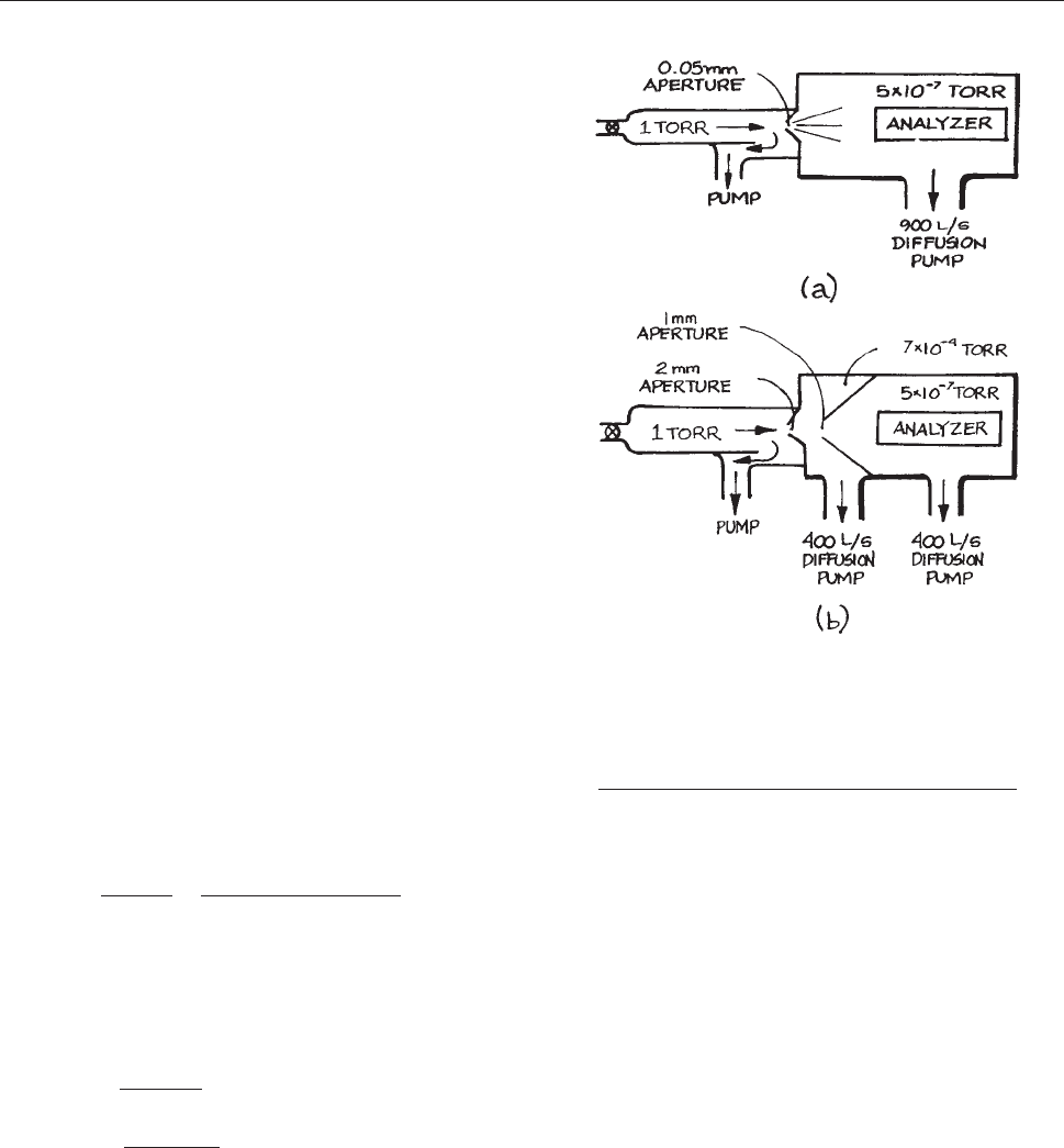
Company) is used as a small UHV chamber. The pump is
mounted on one face and the remaining five faces provide
ports for mounting components. The cube was ordered 0.5
in oversize (i.e., 6.5 in. 3 6.5 in. 3 6.5 in.). With the addi-
tional size it is possible to bore .375 in diameter holes
through the cube close to each vertical edge. Cartridge
heaters inserted in the holes are used for bakeout.
3.6.2 Differential Pumping
One is occasionally required to design a system wherein gas
is maintained at two very different pressures. Often two or
more pumps with interconnecting tubing must be balanced
against one another to obtain the desired pressure differential.
As an example we will consider the problem of making
a mass-spectrometric analysis o f trace constituents in
argon flowing through a t ube at a pressure P
0
of 1.0 tor r.
As illustrated schematically in Figu re 3.33(a),thesample
is
to be withdrawn through a hole in the flow tube. The
mass s pectrometer must be operated at a pressure P
2
of
5 3 10
7
torr. To begin, let us suppose that a 6 in. diffusion
pump is to be used to maintain the pressure P
2
. A properly
trapped 6 in. diffusion pump has a speed of about 900 L s
1
over the range 10
3
–10
9
torr (see Figure 3.12). The
throughput is then:
Q ¼ P
2
S ¼ð5 3 10
7
torrÞð900 L s
1
Þ
¼ 4:5 3 10
4
torr L s
1
ð3:38Þ
The conductance of the sampling aperture that provides
this throughput is:
C ¼
Q
P
0
P
2
¼
4:5 3 10
4
torr L s
1
1:0 torr
¼ 4:5 3 10
4
Ls
1
ð3:39Þ
The flow through this aperture is in the viscous-flow
regime. The area of the aperture that provides this conduc-
tance (from Section 3.2.4) is approximately:
A ¼
C Ls
1
ðÞ
20
cm
2
¼
4:5 3 10
4
20
¼ 2:3310
5
cm
2
ð3:40Þ
corresponding to a diameter of 0.05 mm for a circular
aperture. There ar e two problems associated with this
small aperture. Firstly, there is the mechanical difficulty
of creating suc h a small hole . Secondly, this tiny hole
may impose a severe limitation upon the sensitivity of
the measurement, particularly if the analyzer samples
only atoms moving along the line of sight from aperture
to analyzer. A solution to these problems is to incorpo-
rate several stages of pumping – a scheme known as
differential pumping.
A two-stage differentially pumped system is illustrated
in Figure 3.33(b). An intermediate-pressure chamber with
its
own pump is interposed between the sample and ana-
lyzer volumes. There are two apertures now and the pres-
sure drop occurs in two steps. For comparability with the
previous example, suppose the intermediate chamber
and the analyzer chamber are each evacuated with 4 in.
Figure 3.33 (a) Schematic representation of
an analyzer in high vacuum (5 x 10
7
torr) used
to sample a gas at high pressure (1 torr).
(b) Differential pumping arrangement that
permits a much larger sampling aperture with
the same total pumping speed for the analyzer.
138 VACUUM TECHNOLOGY

diffusion pumps, each with a speed of 400 L s
1
. Take the
ratio of pressures across each aperture to be the same, so
that P
0
/P
1
¼ P
1
/P
2
and the pressure P
1
in the intermediate
chamber is then 7 3 10
4
torr. The throughput of the pump
on the lowest pressure chamber is:
Q
2
¼ P
2
S
¼ð5 3 10
7
torrÞð400 L s
1
Þ
¼ 2 3 10
4
torr L s
1
ð3:41Þ
The conductance C
2
of the aperture separating the region
of pressure P
1
from the region of pressure P
2
must main-
tain this throughput:
C
2
¼
Q
2
P
1
P
2
¼
2 3 10
4
torr L s
1
7 3 10
4
torr
¼ 0:3Ls
1
ð3:42Þ
The flow through this aperture is in the molecular-flow
regime. The area of the aperture that provides this conduc-
tance (from Section 3.2.4) for argon at 300 K is:
A
2
¼ C 3:7
T
M
1=2
"#
1
cm
2
¼ 0:03 cm
2
ð3:43Þ
corresponding to a diameter of about 2 mm for a circular
aperture. Similarly, the conductance of the aperture sepa-
rating the high- and intermediate-pressure regions must
match the throughput of the intermediate pump:
Q
1
¼ P
1
S
¼ð7 3 10
4
torrÞð400 L s
1
Þ
¼ 0:3 torr L s
1
ð3:44Þ
so that:
C
1
¼
Q
2
P
0
P
1
¼
0:3 torr L s
1
1 torr
¼ 0:3Ls
1
ð3:45Þ
The flow through this aperture is in the viscous-flow
regime. The area of the aperture that provides this conduc-
tance (from Section 3.2.4) is approximately:
A
1
¼
C Ls
1
ðÞ
20
cm
2
¼
0:3
20
¼ 0:015 cm
2
ð3:46Þ
corresponding to a diameter of about 1 mm for a circular
aperture. In this example, we find that, by pumping in
stages, and without an increase in total pumping speed,
the required pressure differential can be maintained across
apertures that are hundreds of times larger than if all the
available pumping speed had been applied in a single
stage. Furthermore, assuming that the gas flow through
first aperture is directional, the sensitivity of the measure-
ment is greatly increased by aligning the second aperture
and analyzer with the flow through the first aperture, as
suggested in the figure.
3.6.3 The Construction of
Metal Vacuum Apparatus
Metal vacuum chambers are often built up of one or more
cylindrical sections. Tube stock is readily available and a
cylindrical shape is second only to a spherical shape in
strength to withstand external pressure. Even when tube
stock is unavailable, a cylindrical section is easily fabri-
cated by rolling up sheet stock. The ends of a cylindrical
chamber are most conveniently closed with flat plates, as
shown in Figure 3.34. A flat end plate must be quite thick
to
withstand atmospheric pressure, as discussed below.
Domed or spherical end caps are much stronger, but more
expensive to fabricate.
The ability of a cylinder to resist collapsing under external
pressure depends upon the length of the cylinder between
supporting flanges, the diameter, the wall thickness, and the
strength of the material. The ASME has published standards
for the wall thickness of cylindrical vessels under external
pressure.
17
The data in Figure 3.35 have been abstracted
from the ASME specifications for type 3003-T0 aluminum
alloy and type 304 stainless steel respectively. These recom-
mendations should be more than adequate for any of the
4000, 6000, or 7000 series tempered aluminum alloys (such
as 2024-T4, 6061-T6, or 7075-T6) and adequate for most
VACUUM-SYSTEM DESIGN 139
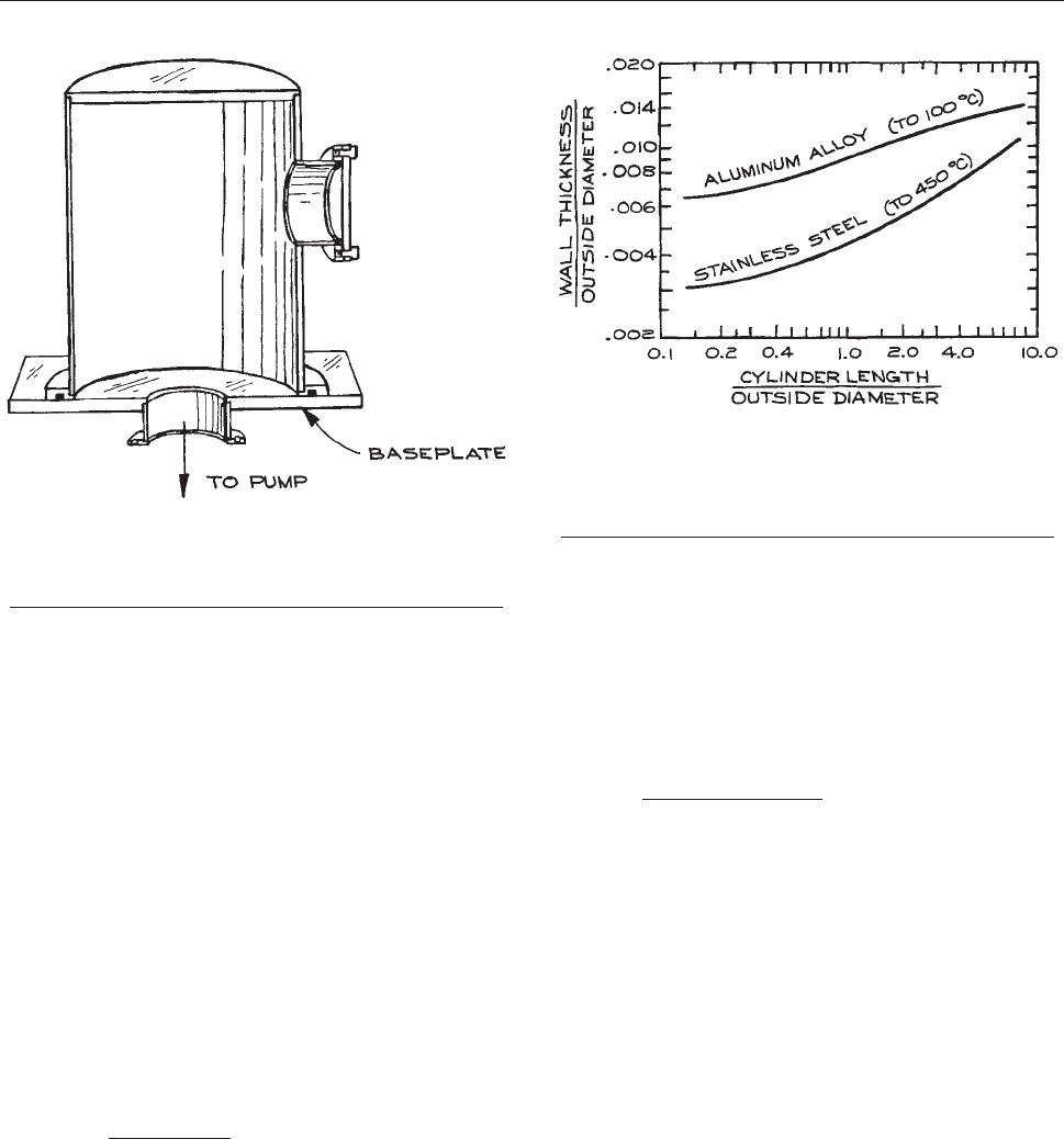
stainless steels. Soft aluminum, such as the 1000-series
alloys, should not be used for vacuum chambers. Holes
cut for ports in the side of a cylinder reduce the strength
of the cylinder and should be avoided. If side ports are
necessary, the wall thickness should be increased over the
recommendations of the code. Dents and out-of-roundness
in a cylinder weaken it and should be avoided.
A flat end plate will bend a surprising amount under
atmospheric pressure. Assuming the plate caps a cylindri-
cal shape, the nature of the stress in the plate and the
maximum deflection depend upon whether or not the edges
of the plate are clamped to the cylinder. In this case
‘‘clamped’’ implies that the plate is welded to the cylinder.
A removable end plate bolted in place should be consid-
ered ‘‘unclamped’’ when designing a vacuum chamber.
The deflection at the center of a flat circular end plate
clamped at its edges is:
d ¼
3PR
4
ð1 l
2
Þ
16Ed
3
ðedge clampedÞð3:47Þ
where P the external pressure, R is the radius of the plate, d
the thickness, l Poisson’s ratio, and E the modulus of
elasticity or Young’s modulus of the material.
18
In this
case, the maximum tensile stress is at the edge of the plate
(see Section 1.6.3).
The
deflection of a demountable end plate is greater than
that of a permanent end cap. For a circular plate with
unclamped edges:
d ¼
3PR
4
ð5 þ lÞð1 lÞ
16Ed
3
ðunclampedÞð3:48Þ
The maximum stress is at the center of the plate (see
Section 1.6.3).
T
he deflection of flat end plates of steel or aluminum
under atmospheric pressure is plotted in Figure 3.36. In most
ca
ses, relative deflection, (d/R), in the range 0.001 to 0.005
should be acceptable, otherwise the plate may be too heavy.
Steel is about three times more dense than aluminum. For a
given maximum deflection, an aluminum plate is less than
half as heavy as a steel plate. A vacuum-chamber design that
incorporates a stainless-steel cylinder with a demountable
aluminum end plate has much to say in its favor. Welds in
the stainless cylinder are much stronger and more reliable
than would be the case if the cylinder were made of alumi-
num. A removable aluminum end plate is lighter and much
less expensive to machine than one of steel.
Figure 3.34 Typical aluminum or steel vacuum chamber
resting on a baseplate. The pump, gauges, and electrical
and mechanical feedthroughs are most conveniently
mounted to the baseplate.
Figure 3.35 Recommended minimum wall thickness
(scaled to diameter) for evacuated aluminum-alloy
and stainless-steel tubes under external atmospheric
pressure, as a function of tube length (scaled to
diameter) between supporting flanges.
140 VACUUM TECHNOLOGY
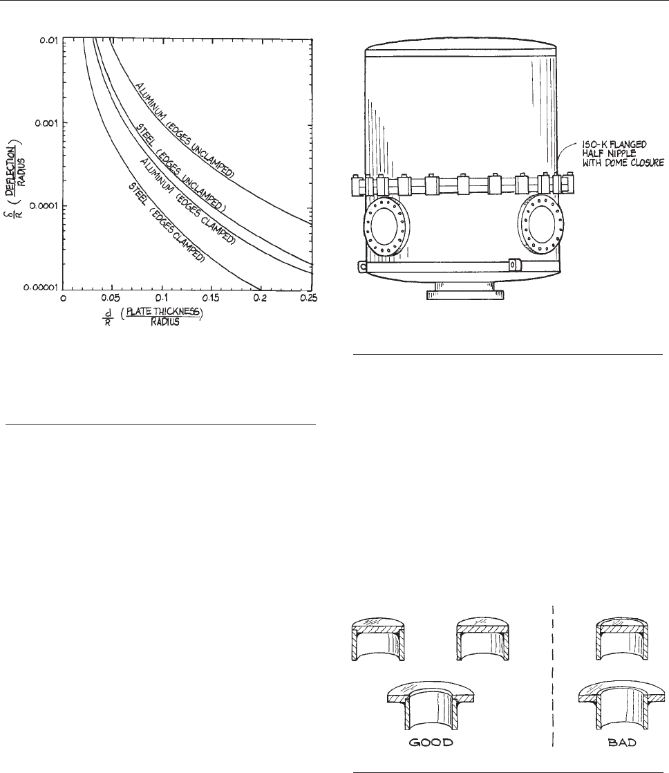
The deflection of the walls of a vacuum chamber must be
accounted for in designing the mounting for a vacuum sys-
tem. If both the chamber and the pump are securely
mounted, severe stresses will dev elop as the chamber is
evacuated. The correct practice is to securely mount the
vacuum chamber and leave the pump suspended from a
flange on the chamber , or, alternati v ely, to mount the pump
and permit the chamber to rest on top of the pump with no
further constraint. In the latter case, it is important that forces
generated by the apparatus resting on the top of the pump do
not distort the pump. This is particularly important for
pumps requiring a high degree of mechanical precision, such
as a turbomolecular pump or a molecular drag pump. It is
generally recommended that turbopumps and drag pumps be
suspended by their inlet flange with no other attachment.
Using standard, commercially av ail able components save s
both time and money. In fact, even quite large systems can
be built entirely of standard parts. In the author’s laboratory
a chamber 50 cm (20 in.) in diameter and 100 cm (40 in.)
high was created from a pair of ISO 500 half nipples that
were ordered with domed end caps. Ports were added to the
lower half nipple for feedthroughs and for a pump, as shown
in Figure 3.37. The total cost was about $5000 in 1994.
Me
tal parts may be joined by soldering, brazing, or weld-
ing. Tungsten – inert-gas welds (so-called ‘‘TIG’’ or ‘‘heli-
arc’’ welds) produce the cleanest, strongest joints in stainless
steel. Soldering and brazing result in less distortion of the
joined parts and are more convenient operations in the labo-
ratory. As shown in Figure 3.38, a joint that is to be soldered
or
brazed should be designed so that the metal parts take the
thrust of the atmosphere and the solder or brazing alloy
serves only as a sealant. If possible, the joint should be
Figure 3.36 Deflection of flat circular plates under
atmospheric pressure. A clamped end plate caps a cylindrical
tube and is welded in place, otherwise the plate should be
considered as unclamped. These curves assume a Poisson’s
ratio of 0.3 and a Young’s modulus of 210 GN m
2
(3 3 10
7
psi) for steel and 70 GN m
2
(1 3 10
7
psi) for aluminium.
Figure 3.37 A vacuum chamber composed of a pair of
ISO-500 (500 mm diameter) half nipples with domed
end caps.
Figure 3.38 The design of joints to be soldered or brazed.
VACUUM-SYSTEM DESIGN 141
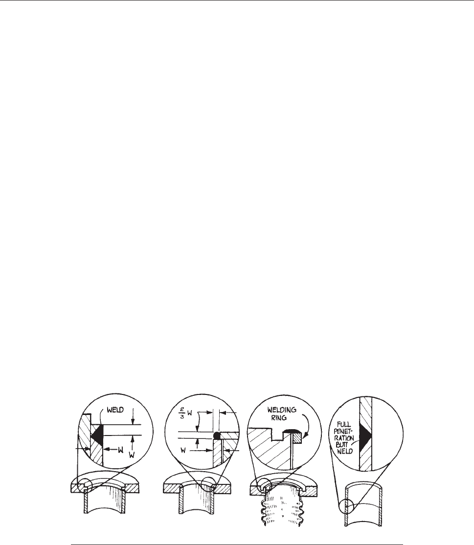
designed to provide positive location of mating parts. The
surfaces to be joined should be cleaned before assembly by
sandblasting or by polishing with sandpaper so that the sol-
der or brazing metal will flow into and completely fill the
joint. This is necessary to achieve maximum strength and to
eliminate a narrow gap that is difficult to pump out and is
liable to collect flux and other material that will contaminate
the vacuum system. Tin-alloy solders (plumbing solder)
should only be used for rough vacuum applications such
as a diffusion-pump foreline. Brazed joints are acceptable
in high vacuum. The copper–silver eutectic alloy is the pre-
ferred brazing material. Brazing is an excellent way of
attaching thin metal parts, such as bellows, that can easily
be burned through in a welding operation.
Welded joints are designed to minimized distortion in
the welding process and to avoid occlusions on the vac-
uum side of the joint that may trap contaminates or a ct as
virtual l eaks. Parts to be joined by welding are designed
so that the rate of heat dissipation while welding is the
same to each part. This is necessary to prevent destruc-
tive thermal stresses from being frozen into the finished
joint. When joining a heavy flange to a thin tube, a notch
or a groove is cut in the thick part near the joint to control
the rate at whic h heat is dissipa ted, as shown in Figure
3.3
9. To join a very thin part to a fl ange, extra material,
such
as the welding ring shown in the figure, is added to
back up the weld. Whenever possible, welds should be
on the vacuum side, that is, on the inside of the vacuum
wall. Locational welds or ‘‘tack welds’’ should be on the
outside and should be intermittent. For material up to about
3 mm (1/8 in.) thick, full-penetration welds should be
specified. A weld from the outside, often necessary when
joining a small diameter tube to a flange, should be a full
penetration weld if possible. When an outside weld is
unavoidable, the joint should be designed to minimize
the trapped volume on the inside, as shown in the figure.
Metal parts inside a vacuum system may be joined by
welding or brazing, but in most cases nut-and-bolt assem-
bly is more convenient. Special care must be taken to
prevent air from being trapped under a screw in a blind
hole. The placement of pumpout holes for blind screw
holes is illustrated in Figure 3.40.
3.6.4 Surface Preparation
Surfaces that are to be exposed to a vacuum should be free
of substances that have a significant vapor pressure, and
they should be as smooth as possible to minimize the
microscopic surface area and thus minimize the amount
of adsorbed gas. The substances that must be removed
from the surfaces of vacuum apparatus are mainly hydro-
carbon oils and greases, and inorganic salts that are hygro-
scopic and outgas water vapor.
The two preferred treatments for metal vacuum-system
surfaces are electropolishing and bead blasting. Con ventional
wheel polishing and buffing is unsatisfactory, since these
processes tend to flatten surface burrs and trap gas under-
neath. Electropolishing is con v eniently carried out in the
laboratory, although most machine shops are prepared to
do it routinely. An electropolishing solution for stainless steel
Figure 3.39 Welded joints in a vacuum system.
142 VACUUM TECHNOLOGY
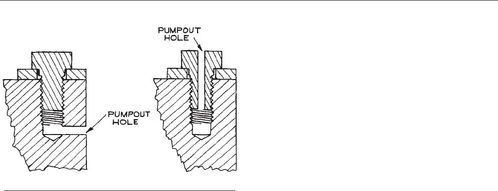
recommended by Armco Steel consists of 50 parts by volume
of citric acid and 15 parts by volu me of sulfuric acid, plus
enough water to make 100 parts of solution. The solution
should be used at a temperature of 90 ºC. A current density of
about 0.1 A/cm
2
at 6 to 12 V is required. A copper cathode is
used with the piece to be polished serving as the anode.
Blasting with 20–30 micron glass beads effectively
reduces the adsorbing area of a metal surface and thus
reduces the rate of outgassing from the surface. Glass
beading can be carried out in a conventional sandblasting
apparatus. The machine should be carefully cleaned of
coarse grits before use.
Shop processes such as welding, plasma cutting, and
high-speed turning can leave surfaces with a heavy layer
of oxides and other contaminants. Bead blasting or, alter-
natively, the chemical process known as pickling may
remove this layer. A pickling solution for stainless steel
consists of 2% (by volume) concentrated nitric acid
(HNO
3
) and 25% hydrochloric acid (HCl) in distilled
water at 60 ºC. This solution is known as ‘‘bright dip’’ in
the shop. After dipping in this solution, the part should be
thoroughly rinsed and its surface neutralized by immersion
in an alkaline solution. Aluminum is pickled in a 10%
solution of sodium hydroxide (NaOH) saturated with com-
mon salt (NaCl) at 80 ºC. After about half a minute in this
solution the part is transferred to a 10% solution of hydro-
chloric acid to obtain a bright finish.
An ultrasonic cleaner is particularly effective for prepar-
ing vacuum parts. The cleaner should be fired with a deter-
gent solution. If two cleaners are available, fill one with
detergent solution and the other with distilled water, and
use them in sequence with a hot-water rinse between.
Diffusion-pump oil is especially difficult to remove.
Nevertheless, a diffusion pump must be thoroughly
cleaned when replacing old oil with new or when changing
from one type of oil to another. Hydrocarbon oils, poly-
phenylethers, and silicone fluids can be dissolved in tri-
chloroethylene followed by acetone and then ethyl alcohol.
Trichloroethylene is somewhat toxic, and acetone and
ethanol are flammable, so this cleaning should be carried
out carefully in a fume hood. Avoid skin contact with these
solvents. Fluorinated diffusion-pump fluids, such as the
perfluoropolyethers (Fomblin), are soluble in fluorinated
solvents such as chlorotrifluoroethane.
Glass can usually be effectively cleaned by washing in a
detergent solution followed by a rinse in hot water and
immersion in a 10–20% solution of hydrofluoric acid.
The glass is then rinsed with water, neutralized with an
alkaline solution, and rinsed with distilled water. Protect
eyes and skin during these operations. Hydrofluoric acid
burns are especially painful and persistent.
After surface treatment as required for particular com-
ponents, the final cleaning procedure for all components of
a vacuum system should proceed as follows:
(1) Scrub with a strong solution of detergent (Alconox or
liquid dishwashing detergent is fine).
(2) Rinse with very hot water.
(3) Rinse with distilled water.
(4) Rinse with pure methanol.
Do not touch clean parts with bare hands. Disposable plas-
tic gloves (free of talc) are convenient for handling vacuum
apparatus after cleaning.
3.6.5 Leak Detection
A leak that raises the base pressure of a system above
about 10
6
torrcanusuallybefoundbyprobingsus-
pected locations on the outside of the vacuum chamber
with a liquid or vapor for which the gauge sensitivity or
pump speed is very different from that for air. A squeeze
bottle of acetone or a spray can of a Freon cleaner is a
useful tool. These liquids w ill usually cause a very abrupt
increase in indicated pressure as they flow through a leak,
Figure 3.40 Pumpout holes for blind screw holes.
VACUUM-SYSTEM DESIGN 143

but somet imes rapid evaporation of a li quid t hrough a
leak will cause the liquid to freeze and temporarily plug
the leak, causing the pressure to fall. A disadvantage of
this method is that the solvent may contaminate O-rings.
A small jet of helium is also a useful leak probe because
an ionization gauge is quite insensitive to helium. The
indicated pressure will fall when helium i s introduced
into a leak.
In a glass system, a leak that raises the pressure into the
10 mtorr to several torr range can be located with a Tesla
coil. The surface of the glass is brushed with the discharge
from the Tesla coil. The discharge is preferentially directed
toward the leak, and a bright white spot will reveal the
location as the discharge passes through. Avoid very thin
glass walls and glass-to-metal seals, as the Tesla discharge
can hole the glass in these fragile areas.
For very small leaks in high-vacuum systems, a mass-
spectrometer leak detector is needed (see Section 3.3.5).
3.6.6 Ultrahigh Vacuum
To achieve pressures much below 10
7
torr, baking is
required to remove water and hydrocarbons from vac-
uum-system walls. Heating to 50–100 ºC for several hours
will improve the ultimate pressure of most systems by an
order of magnitude. A true ultrahigh-vacuum system must
be baked to at least 250 ºC for several hours during the
initial pump out. A system contaminated with hydrocar-
bons may require a bakeout at temperatures approaching
400 ºC. After a hard preliminary bake in vacuo to remove
deeply adsorbed material, the system can be baked more
gently after subsequent exposures to air.
A small system can be wrapped with heating tape and
then covered with fiberglass insulation. For larger systems,
an oven constructed of sheet metal insulated with fiber-
glass can be erected around the vacuum chamber and
heated with bar heaters. Batts of fiberglass insulation
intended for use in automobile engine compartments are
readily available. Do not use home-insulating fiberglass
materials. Metal seals must be used in a metal vacuum
system that is to be baked. It is, however, often necessary
to join the vacuum chamber to its pumping station with an
O-ring-sealed flange. In this case, a cooling coil should be
installed around the flange (as in Figure 3.23) to prevent
damage
to the O-ring while the chamber is being baked.
Alternatively a metal O-ring can be used, as described in
Section 3.5.2.
Quartz
lamp heaters can be installed inside a vacuum
system to directly heat the surfaces that need to be out-
gased. This method is frequently faster and more econom-
ical than heating from the outside. A recent innovation for
removing water absorbed on the walls of vacuum appara-
tus employs ultraviolet radiation rather than heat. A lamp
known as a Phototron, manufactured by Danielson, is
inserted in the vacuum system. This lamp radiates at a wave-
length absorbed by water molecules and imparts sufficient
energy to break the bond holding the water to the walls. This
method is not so effective as a high-temperature bakeout,
since the radiation is fairly specific for water and, in addi-
tion, the radiation cannot be expected to penetrate into small
involutions where water may be trapped. The method is
faster than a thermal bakeout and can be used in a system
that contains materials that are degraded by heat. It is
claimed to be 80 to 90% as effective as a bakeout.
Hydrocarbons from pump oils, cleaning fluids and shop
processes are ubiquitous contaminates in vacuum systems.
Hydrocarbons create insulating layers on electrodes in elec-
tron microscopes and mass spectrometers. Their presence is
a particular problem in mass spectrometer experiments
since the hydrocarbon spectrum is very rich. XEI Scientific
has developed a device (the Evactron) that produces a low-
pressure plasma in oxygen to make radicals that react with
hydrocarbons in the vacuum system leaving only low-
vapor-pressure residues (‘‘ash’’).
To reduce outgassing to a minimum in an ultrahigh-
vacuum system it is common practice to prefire (‘‘stove’’)
components before they are assembled, in order to clean
the surfaces and to drive out dissolved gases. The usual
shop practice is to fire components in a hydrogen atmos-
phere such as is provided by a hydrogen furnace or a dis-
sociated-ammonia furnace. This has the advantage of
effectively removing oxides from surfaces. The disadvant-
age to this procedure is that hydrogen is left to outgas at
lower temperatures. Copper parts containing trapped or
dissolved oxygen are also subject to embrittlement as a
result of hydrogen firing. It is for this reason that oxy-
gen-free high-conductivity (OFHC) copper should be used
in constructing vacuum apparatus. High-temperature bak-
ing in vacuum or under an inert atmosphere is the preferred
treatment. Iron, steel, stainless-steel, and nickel-alloy parts
144 VACUUM TECHNOLOGY

are fired at a temperature of about 900 ºC for up to eight
hours. Copper is fired at 500 ºC.
Cited References
1. N. Milleron, Res. Dev., 21(9), 40, 1970.
2. Derivations of the conductance formulae are given by C. M.
VanAtta, Vacuum Science and Engineering, McGraw-Hill,
New York, 1965, pp. 44–62 and J. F. O’Hanlon, A User’s
Guide to Vacuum Technology, 2nd edn., John Wiley & Sons,
Inc., New York, 1989, Chap. 3.
3. M. A. Biondi, Rev. Sci. Instr., 24, 989, 1953.
4. A. T. J. Hayward, J. Sci. Instr., 40, 173, 1963; C. Veillon,
Rev. Sci. Instr., 41, 489, 1970.
5. H. Ishii and K. Nakayama, Transactions of the 2nd
International Congress on Vacuum Science and
Technology, Vol. 1, Pergamon Press, Elmsford, NY, 1961, p.
519; R. J. Tunnicliffe and J. A. Rees, Vacuum, 17, 457,
1967; T. Edmonds and J. P. Hobson, J. Vac. Sci. Tech., 2,
182, 1965.
6. G. R. Brown, P. J. Sowinski, and R. Pertel, Rev. Sci. Instr.,
43, 334, 1972.
7. An application of this process is described by J. H. Moore
and C. B. Opal, Space Sci. Instr., 1, 377, 1975.
8. C. B. Lucas, Vacuum, 23, 395, 1973.
9. R. H. Jones, D. R. Olander, and V. R. Kruger, J. Appl. Phys.,
40, 4641,1969; D. R. Olander, J. Appl. Phys ., 40, 4650,
1969; D. R. Olander, J. Appl. Phys., 41, 2769, 1970; D. R.
Olander, R. H. Jones, and W. J. Siekhaus, J. Appl. Phys., 41,
4388, 1970; W. J. Siekhaus and R. H. Jones, J. Appl. Phys.,
41, 4392, 1970.
10. M. G. Liverman, S. M. Beck, D. L. Monts, and R. E.
Smalley, J. Chem. Phys., 70, 192, 1979; W. R. Gentry and
C. F. Giese, Rev. Sci. Instr., 49, 595, 1978; C. M. Lovejoy
and D. J. Nesbitt, J. Chem. Phys., 86, 3151, 1987.
11. D. Bassi, S. Iannotta, and S. Niccolini,
Rev. Sci. Instr., 52,8
,
1981; F. M. Behlen, Chem. Phys. Lett., 60, 364, 1979.
12. R. E. Smalley, D. H. Levy, and L. Wharton, J. Chem. Phys.,
64, 3266, 1976.
13. J. B. Anderson, R. P. Andres, and J. B. Fenn, in Advances in
Chemical Physics,Vol.10,Molecular Beams, J. Ross (Ed.),
John Wiley & Sons, Inc., New York, 1966, Chapter 8; H.
Pauly and J. P. Toennies, in Methods of Experimental
Physics, Vol. 7, Part A, B. Bederson and W. L. Fite, (Eds.),
Academic Press, New York, 1968, Chapter 3.1; D. R. Miller,
in Atomic and Molecular Beam Methods, Vol. I, G. Scoles,
(Ed.), Oxford University Press, Oxford, 1988, pp. 14–53.
14. W. D. Kingery, H. K. Bowen, and D. R. Uhlmann,
Introduction to Ceramics, 2nd edn., John Wiley & Sons,
Inc., New York, 1976, Chapter 17.
15. J. F. O’Hanlon, A User’s Guide to Vacuum Technology, 3rd
edn., Wiley, Hoboken, NJ, 2003, pp. 366–369.
16. This system is an adaptation of a design described by N. W.
Robinson, Ultra-high Vacuum, Chapman and Hall, London,
1968, pp. 72–73.
17. A.S.M.E. Boiler and Pressure Vessel Code, Section VIII,
Division 1, Appendix V, 1974.
18. Clifford Mathews, A.S.M.E. Engineer’s Data Book, 2nd
edn., ASME Press, NY, 2001, p. 75; J. F. Harvey, Pressure
Vessel Design, Van Nostrand, Princeton, NJ, 1963, pp.
89–91.
General References
Comprehensive Texts on
Vacuum Technology
S. Dushman, Scientific Foundations of Vacuum Technique,
2nd edn., J. M. Lafferty (Ed.), John Wiley & Sons Inc.,
New York, 1961.
M. Hablanian, High-Vacuum Technology, Dekker, New York,
1990.
G. Lewin, Fundamentals of Vacuum Science and Technology,
McGraw-Hill, New York, 1965.
J. F. O’Hanlon, A User’s Guide to Vacuum Technology, 3rd edn.,
Wiley, Hoboken, NJ, 2003.
J. M. Lafferty (Ed.), Foundations of Vacuum Science
and Technology, Joh n Wiley & Son s, In c., New York,
1998.
C. M. Van Atta, Vacuum Science and Engineering, McGraw-Hill,
New York, 1965.
‘‘Vacuum Technology: Its Foundations, Formulae and Tables’’,
until 1996 published as an appendix of the Leybold AG
catalog, Product and Vacuum Technology Reference Book,
Leybold, Inc., San Jose, CA.
Detailed Calculation of Gas Flow
R. A. Roth, Vacuum Technology, 2nd edn., North-Holland,
Amsterdam, 1982.
R. G. Livesey, ‘‘Flow of Gases through Tubes and Orifices’’ in
Foundations of Vacuum Science and Technology, J. M. Lafferty
(Ed.), John Wiley & Sons, Inc., New York, 1998.
REFERENCES 145

Design of Vacuum Systems
N. T. M. Dennis and T. A. Heppell, Vacuum System Design,
Chapman and Hall, London, 1968.
G. W. Green, The Design and Construction of Small Vacuum
Systems, Chapman and Hall, London, 1968.
R. P. LaPelle, Practical Vacuum Systems, McGraw-Hill,
New York, 1972.
Outgassing Data
W. A. Campbell, Jr., R. S. Marriott, and J. J. Park,
A Compilation of Outgassing Data for Spacecraft Materials,
NASA Technical Note TND-7362, NASA, Washington,
DC, 1973.
Properties of Materials Used in Vacuum
Systems
W. Espe, Materials of High Vacuum Technology: Vol. 1, Metals
and Metaloids; Vol. 2, Silicates; Vol. 3, Auxiliary Materials,
Pergamon Press, Oxford, 1968 (a translation of the original
German published in 1960).
Sealing Ceramics and Glass to Metal,
Heat-Treating, Cleaning, Building Joints,
and Feedthroughs
F. Rosebury, Handbook of Electron Tube and Vacuum
Techniques, Addison-Wesley, Reading, Mass., 1969.
A. Roth, Vacuum Sealing Techniques, Pergamon Press,
New York, 1966 and American Vacuum Society Classics,
American Institute of Physics, New York, 1994.
Ultrahigh Vacuum
P. A. Redhead, J. P. Hobson, and E.V. Kornelsen, The
Physical Basis of Ultrahigh Vacuum, Chapman and Hall,
London, 1968.
R. W. Roberts and T. A. Vanderslice, Ultrahigh Vacuum and
Its Applications, Prentice-Hall, Englewood Cliffs, NJ, 1963.
W. Robinson, The Physical Principles of Ultrahigh Vacuum
Systems and Equipment, Chapman and Hall, London, 1968.
G. F. Weston, Ultrahigh Vacuum Practice, Butterworths, London,
1985.
J. T. Yates, Jr., Experimental Innovations in Surface Science,
Springer-Verlag, New York, 1998.
146 VACUUM TECHNOLOGY

OPTICAL SYSTEMS
Physical, chemical, and biological phenomena are regu-
larly studied or induced optically. Such experiments can
involve light absorption, light emission, or light scattering.
We can characterize any experimental arrangement where
light is used, produced, measured, modified, or detected as
an overall optical system. Any such optical system will
always be reducible to three parts: a source of light, a
detector of that light, and everything in between. We will
frequently refer to this important and varied intermediary
arrangement as the optical system. Consequently, our dis-
cussion of overall optical system design and construction
will involve three key topics: sources, optical systems, and
detectors (to be discussed in detail in Chapter 7). The light
source may be a laser, lamp, light-emitting diode, or the
Sun. The detector may be a vacuum tube, solid-state device,
or even the eye. Light intensity may vary from continuous
wave (CW) to pulsed, and these pulses may have durations
as short as a few femtoseconds. Passive elements in the
system may transmit, reflect, combine, polarize, or sepa-
rate light according to its spectral content. Nonlinear opti-
cal elements change the spectral content of light.
It is our aim in this chapter to explain the basic concepts
that need to be understood by the experimentalist who uses
optical techniques. In addition, we will provide examples
of useful techniques for producing, controlling, analyzing,
and modulating light.
4.1 OPTICAL TERMINOLOGY
Light is one form of electromagnetic radiation, the many
categories of which make up the electromagnetic spectrum.
Electromagnetic radiation, which transports energy from
point to point at the velocity of light, can be described in
terms of both wave and particle ‘‘pictures’’ or ‘‘models’’.
This is the famous ‘‘wave-particle’’ duality of all fields or
particles in our model of the Universe. In the electromag-
netic-wave picture, waves are characterized by their fre-
quency m, wavelength k, and the velocity of light c, which
are related by c ¼ mk. A propagating electromagnetic wave
is characterized by a number of field vectors, which vary in
time and space. These include the electric field E (meas-
ured in Volt/m), the magnetic field H (measured in Amp/
m), the displacement vector D (measured in Coulomb/m
2
,
and the magnetic flux density B (measured in Webers/m
2
or Tesla). For a complete description the polarization state
of the wave must also be specified. Linearly polarized
waves have fixed directions for their field vectors, which
do not re-orient themselves as the wave propagates. Circu-
lar or elliptically polarized waves have field vectors that
trace out circular or elliptic helical paths as the wave trav-
els along. In the particle picture, electromagnetic energy is
carried from point to point as quantized packets of energy
called photons. The energy of a photon of frequency m is hm,
where h is Planck’s constant – 6.626 3 10
–34
J s. Photons
have zero mass, travel at the velocity of light, and also carry
both linear and angular momentum. The linear momentum
of a photon of wavelength is p ¼ h/k, the angular momen-
tum depends on the equivalent polarization state of the cor-
responding wave. Circularly polarized photons have angular
momentum h/2p ¼
-
.
Our everyday experience of ‘‘light’’ generally only
encompasses the small part of the electromagnetic spectrum
to which the human eye is sensitive, a wavelength range
running roughly from 400–700 nm. The full electromagnetic
147
CHAPTER
4

spectrum, going from low to high frequencies, is divided
into radiowaves (0–1 GHz), microwaves (1–300 GHz),
infrared waves (k 0.7 –1000 lm) (300 GHz–430 THz)
a
visible light (k 400–700 nm), ultraviolet light (k 10–
400 nm), X-rays (k 0.1–10 nm), and c waves (k < 0.1 nm).
The wavelength region between 10 nm and 200 nm is
often called the vacuum-ultraviolet region because these
wavelengths are absorbed by air and most gases. Optical
systems can somewhat arbitrarily be classified as systems
that handle light in the spectral region between 10 nm and
100 lm. Beyond the far-infrared, between 100 and 1000 lm
(the submillimeter wave region of the spectrum), lies a
spectral region where conventional optical methods can still
be used, but become difficult, as does the extension of
microwave techniques for the centimeter- and millimeter-
wave regions. The use of optical techniques in this region,
and even in the millimeter region, is often called quasi-
optics.
1–4
Only a few experimental techniques and devices
that are noteworthy in this region will be mentioned.
Table 4.1 summarizes the important parameters that are
used
to characterize light and the media through which it
passes. A few comments on the table are appropriate.
Table 4.1 Fundamental parameters of electromagnetic radiation and optical media
Parameter Symbol Value Units
Velocity of light in tacuo c
0
¼(l
0
e
0
)
1/2
2.99792458 3 10
8
m/sec
Permeability of free space l
0
4p 3 10
7
henry/m
Permittivity of free space e
0
8.85416 3 10
12
farad/m
Velocity of light in a medium c ¼(l
r
l
0
e
r
e
0
)
1/2
¼c
0
/n m/sec
Refractive index n ¼(l
r
e
r
)
1/2
(dimensionless)
Relative permeability of a medium l
r
Usually 1 (dimensionless)
Dielectric constant of a medium e
r
(dimensionless)
Frequency m ¼c/k Hz
10
9
Hz ¼1 GHz (gigahertz)
10
12
Hz ¼1 THz (terahertz)
Wavelength in tacuo k
0
¼c
0
/m
Wavelength in a medium k ¼c/m ¼ k
0
/n m
10
3
m ¼1 mm (millimeter)
10
6
m ¼1 lm (micrometer)
¼1 l (micron)
10
9
m ¼1 nm (nanometer)
¼1ml (millimicron)
10
12
m ¼1 pm (picometer)
10
10
m ¼1 A (Angstrom)
Wavenumber
m ¼ 1=k cm
1
(kayser)
Wavevector k,|k| ¼2p/k m
1
Photon energy E ¼hm J
1.60202 3 10
19
J ¼1eV
(electron volt)
Electric field of wave E V/m
Magnetic field of wave H A/m
Poynting vector P ¼E 3 H W/m
2
Intensity I ¼ <|P|>
at
¼|E|
2
/2Z W/m
2
Impedance of medium
Z ¼
E
x
H
y
¼
E
y
H
x
¼
l
r
l
0
e
r
e
0
1=2
X
Impedance of free space Z
0
¼(l
0
/e
0
)
1/2
376.7 X
148 OPTICAL SYSTEMS
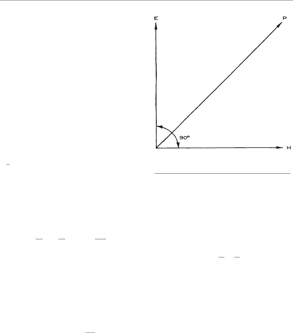
Although the v elocity of light in a medium depends both on
the relative magnetic permeability l
r
, and dielectric constant
e
r
of the medium, for all practical optical materials l
r
¼1, so
the refractiv e index and dielectric constant are related by:
n ¼
ffiffiffiffi
e
r
p
ð4:1Þ
When light propagates in an anisotropic medium, such
as a crystal of lower than cubic symmetry, n and e
r
will, in
general, depend on the direction of propagation of the
wave and its polarization state. The velocity of light in
vacuo is currently the most precisely known of all the
physical constants – its value is known
5
within 40 cm/s.
A redefinition of the meter has been adopted
6
based on the
cesium-atomic-clock frequency standard
7
and a velocity of
light in a vacuum of exactly 2.99792458 3 10
8
m/s. Con-
sequently, the meter is now a derived SI unit, defined as the
distance traveled in vacuo by light in 1/2.99792458 3 10
8
seconds. The velocity, wavelength, and wavenumber of
light traveling in the air have slightly different values than
they have in vacuo. Tables that give corresponding values
of
m in vacuo and in standard air are available.
8
A plane electromagnetic wave traveling in the z-direc-
tion can, in general, be decomposed into two independent,
linearly polarized components. The electric and magnetic
fields associated with each of these components are them-
selves mutually orthogonal and transverse to the direction
of propagation. They can be written as (E
x
, H
y
) and (E
y
,
H
x
). The ratio of the mutually orthogonal E and H compo-
nents is called the impedance Z of the medium:
E
x
H
y
¼
E
y
H
x
¼ Z ¼
ffiffiffiffiffiffiffiffiffi
l
r
l
0
e
r
e
0
r
ð4:2Þ
Most optical materials have l
r
¼ 1. The negative sign in
Equation (4.2) arises because (y, x, z)
is not a right-handed
coordinate system. The Poynting vector:
P ¼ E 3 H ð4:3Þ
is a vector that points in the direction of energy propaga-
tion of the wave, as shown in Figure 4.1. The local direc-
tion
of the Poynting vector at a point in a medium is called
the ray direction. The average magnitude of the Poynting
vector is called the intensity and is given by:
I ¼ <jPj>
av
¼
jEj
2
2Z
ð4:4Þ
The factor of two comes from time-averaging the square
of the sinusoidally varying electric field.
The wavevector k points in the direction p erpendicu-
lar to the phase front of the wave (the surface of cons tant
phase). In an isotropic medium k and P are always
parallel.
The photon flux corresponding to an electromagnetic
wave of average intensity I and frequency v is:
N ¼
I
hv
¼
Ik
hc
ð4:5Þ
where h is Planck’s constant, 6.6 3 10
–34
J s. For a
wave of intensity 1 Wm
2
and wavelength 1 lm in vacuo,
N ¼ 5.04 3 10
18
photons sec
–1
m
–2
. Photon energy is
sometimes measured in electron volts (eV): 1 eV ¼
1.60202 3 10
–19
J. A photon of wavelength 1 lm has an
energy of 1.24 eV. It is often important, particularly in the
infrared, to know the correspondence between photon and
thermal energies. The characteristic thermal energy at
absolute temperature T is kT. At 300 K, kT ¼ 4.14 3
10
–21
J ¼ 208.6 cm
–1
¼ 0.026 eV.
Figure 4.1 Orientation of the mutually orthogonal
electric-field vector E, magnetic-field vector H,
and Poynting vector P.
OPTICAL TERMINOLOGY 149
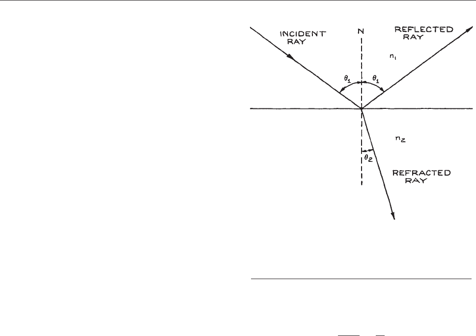
4.2 CHARACTERIZATION AND
ANALYSIS OF OPTICAL
SYSTEMS
Before embarking on a detailed discussion of the properties
and uses of passive optical components and systems con-
taining them, it is worthwhile reviewing some of the param-
eters that are important in characterizing passive optical
systems and some of the methods that are useful in analyz-
ing the way in which light passes through an optical system.
Optical materials have refractive indices that vary with
wavelength. This phenomenon is called dispersion. It causes
a wavelength dependence of the properties of an optical
system containing transmissive components. The change of
index with wavelength is very gradual, and often negligible,
unless the wavelength approaches a region where the mate-
rial is not transparent. Most materials exhibit normal disper-
sion, where the refracti v e inde x decreases with wavelength.
In specific spectral regions they may exhibit anomalous dis-
persion, where the refractiv e index increases with wave-
length over a limited range of wavelengths. A description
of the performance of an optical system is often simplified
by assuming that the light is monoch romatic (light that con-
tains only a small spread of wavelength components).
4.2.1 Simple Reflection and
Refraction Analysis
The phenomena of reflection and refraction are most easily
understood in terms of plane electromagnetic waves –
those in which the direction of energy flow (the ray direc-
tion) is unique. Other types of wave, such as spherical
waves and Gaussian beams, are also important in optical
science; however, the part of their wavefront that strikes an
optical component can frequently be approximated as a
plane wave, so plane-wave considerations of reflection
and refraction still hold true.
When light is reflected from a plane mirror, or the planar
boundary between two media of different refractive index,
the angle of incidence is always equal to the angle of
reflection, as shown in Figure 4.2. This is the fundamental
law
of reflection.
When a light ray crosses the boundary between two
media of different refractive index, the angle of refraction
h
2
, shown in Figure 4.2, is related to the angle of incidence
h
1
by Snell’s law:
sin h
1
sin h
2
¼
n
2
n
1
ð4:6Þ
This result is modified if one or both of the media is
anisotropic.
If n
2
< n
1
there is a maximum angle of incidence for
which there can be a refracted wave, since sin h
2
cannot be
greater than unity for a real angle. This is called the critical
angle h
c
and is given by:
sin h
c
¼n
2
=n
1
ð4:7Þ
as illustrated in Figure 4.3(a)
If h
1
exceeds h
c
, the boundary acts as a very good mirror,
as illustrated in Figure 4.3(b). This phenomenon is called
to
tal internal reflection. Several types of reflecting prisms
discussed in Section 4.3.4 operate this way. When total
internal reflection occurs, there is no transmission of energy
through the boundary. The fields of the wave do not, how-
ever, go abruptly to zero at the boundary. There is an evan-
escent wave on the other side of the boundary, the field
Figure 4.2 Reflection and refraction of a light ray at the
boundary between two different isotropic media of
refractive indices n
1
and n
2
, respectively. The case shown
is for n
2
> n
1
. The incident, reflected, and transmitted
rays and the surface normal N are coplanar.
150 OPTICAL SYSTEMS
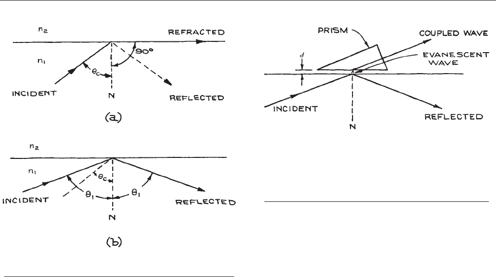
amplitudes of which decay exponentially with distance. For
this reason, other optical components should not be brought
too close to a totally reflecting surface, or energy will be
coupled to them via the evanescent wave and the efficiency
of total internal reflection will be reduced. With extreme
care this effect can be used to produce a variable-reflectivity,
totally internally reflecting surface, as can be seen in Figure
4.
4. Studies of total internal reflection at interfaces are
im
portant in a number of optical measurement techniques,
such as attenuated total (internal) reflection
9
and photon
scanning tunneling microscopy.
10
One or both of the media in Figure 4.2 may be aniso-
tropic, like calcite, crystalline quartz, ammonium dihydro-
gen phosphate (ADP), potassium dihydrogen phosphate
(KDP), or tellurium. Then the incident wave in general
will split into two components, one of which obeys Snell’s
law directly (the ordinary wave) and one for which Snell’s
law is modified (the extraordinary wave). This phenom-
enon is called double refraction.
11–13
If an optical system contains only planar interfaces, the
path of a ray of light through the system can be easily
calculated using only the law of reflection and Snell’s
law. This simple approach neglects diffraction effects,
which become significant unless the lateral dimensions
(apertures) of the system are all much larger than the
wavelength (say 10 times larger). The simple behavior of
light rays in more complex systems containing nonplanar
components, but where diffraction effects are negligible,
can be described with the aid of paraxial-ray analysis.
14,15
Transmitted and reflected intensities and polarization
states cannot be determined by the above methods and
are most easily determined by the method of impedances.
4.2.2 Paraxial-Ray Analysis
A plane wave is characterized by a unique propagation
direction given by the wave vector k. All fields associated
with the wave are, at a given time, equal at all points in
infinite planes orthogonal to the propagation direction. In
real optical systems, ideal plane waves do not exist, as the
finite size of the elements of the system restricts the lateral
extent of the waves. Nonplanar optical components will
cause further deviations of the wave from planarity. Con-
sequently, the wave acquires a ray direction that varies from
point to point on the phase front. The behavior of the optical
system must be characterized in terms of the deviations its
elements cause to the bundle of rays that constitute the
propagating, laterally restricted wave. This is most easily
done in terms of paraxial rays. In a cylindrically symmetric
optical system (for example, a coaxial system of spherical
lenses or mirrors), paraxial rays are those rays whose direc-
tions of propagation occur at sufficiently small angles h to
the symmetry axis of the system that it is possible to replace
Figure 4.3 (a) Critical angle (n
1
> n
2
); (b) total internal
reflection (n
1
> n
2
). N is the surface normal.
Figure 4.4 Schema of an evanescent-wave coupler.
The amount of intensity reflected or coupled is varied by
adjusting the spacing d; shown greatly exaggerated in
the figure. This spacing is typically on the order of the
wavelength. The surface boundary and adjacent prism
face must be accurately flat and parallel.
CHARACTERIZATION AND ANALYSIS 151
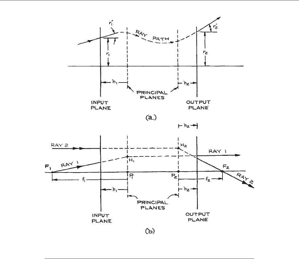
sin h or tan h by h – in other words, paraxial rays obey the
small-angle approximation:
sin h ’ tan h ’ h ð4:8Þ
Matrix Formulation. In an optical system whose
symmetry axis is in the z-direction, a paraxial ray in a
given cross-section (z ¼ constant) is characterized by its
distance r from the z-axis and the angle r9 it makes with
that axis. Suppose the values of these parameters at two
planes of the system (an input and an output plane) are r
1
,
r9
1
and r
2
, r9
2
, respectively, as shown in Figure 4.5(a). Then
in the paraxial-ray approximation, there is a linear relation
between them of the form:
r
2
¼ Ar
1
þ Br
0
1
r
0
2
¼ Cr
1
þ Dr
0
1
ð4:9Þ
or, in matrix notation:
r
2
r
0
2
¼
AB
CD
r
1
r
0
1
ð4:10Þ
Figure 4.5 (a) Generalized schematic diagram of an optical system, showing a typical ray
and its paraxial-ray parameters at the input and output planes; (b) focal points
F
1
and F
2
and principal rays of a generalized optical system.
152 OPTICAL SYSTEMS

Here:
M ¼
AB
CD
ð4:11Þ
is called the ray transfer matrix. If the media where the
input and output ray parameters are measured have the
same refractive index, then the determinant of the ray
transfer matrix is unity, i.e., AD BC ¼ 1.
Optical systems made of isotropic material are generally
reversible – a ray that travels from right to left with input
parameters r
2
, r9
2
will leave the system with parameters r
1
,
r9
1
. Thus:
r
1
r
0
1
¼
A
0
B
0
C
0
D
0
r
2
r
0
2
ð4:12Þ
where the reverse ray transfer matrix is:
A
0
B
0
C
0
D
0
¼
AB
CD
1
ð4:13Þ
The ray transfer matrix allows the properties of an optical
system to be escribed in general terms by the location of its
focal points and principal planes, whose location are deter-
mined from the elements of the matrix. The significance of
these features of the system can be illustrated with the aid of
Figure 4.5(b). An input ray that passes through the fir
st focal
point F
1
(or would pass through this point if it did not first
enter the system) emerges traveling parallel to the axis. The
intersection point of the extended input and output rays,
point H
1
in Figure 4.5(b), defines the location of the first
principal plane. Conversely, an input ray traveling parallel
to the axis will emerge at the output plane and pass through
the second focal point F
2
(or appear to have come from this
point). The intersection of the extension of these rays, point
H
2
, defines the location of the second principal plane. Rays
1and2inFigure 4.5(b) are called the pr
incipal rays of the
system. The location of the principal planes allows the cor-
responding emergent ray paths to be determined, as shown
in Figure 4.5(b). The dashed lines in this figure, which
pe
rmit the geometric construction of the location of output
rays 1 and 2, are called virtual ray paths.BothF
1
and F
2
lie
on the axis of the system. The axis of the system intersects
the principal planes at the principal points, P
1
and P
2
,in
Figure 4.5(b). The distance, f
1
, from the first principal plane
to the first focal point is called the first focal length; f
2
is
called the second focal length.
In many practical situations, the refractive indices of the
media to the left of the input plane (the object space) and to
the right of the output plane (the image space) are equal. In
this case, several simplifications arise:
f
1
¼ f
2
¼ f ¼
1
C
h
1
¼
D 1
C
h
2
¼
A 1
C
ð4:14Þ
h
1
and h
2
are the distances of the input and output planes
from the principal planes, measured in the sense shown in
Figure 4.5(b).
Thus,
if the elements of the transfer matrix are known,
the location of the focal points and principal planes is
determined. Graphical construction of ray paths through
the system using the methods of paraxial ray tracing is
then straightforward (see below).
In using the matrix method for optical analysis, a consis-
tent sign convention must be employed. In the present dis-
cussion, a ray is assumed to trav el in the positi v e z-direction
from left to right through the system. The distance from the
first principal plane to an object is measured positive from
right to left – in the negati v e z-direction. The distance from
the second principal plane to an image is measured positive
from left to right – in the positiv e z-direction. The lateral
distance of the ray from the axis is positiv e in the upward
direction, negati ve in the downward direction. The acute
angle between the system-axis direction and the ray, say r
1
in Figure 4.5(a), is positi v e if a counterclockwise motion is
necessary to go from the positiv e z-direction to the ray direc-
tion. When the ray crosses a spherical interface, the radius of
curvature is positive if the interface is conve x to the input ray.
The use of ray transfer matrices in optical-system analysis
can be illustrated with some specific examples.
(i) Uniform optical medium. In a uniform optical
medium of length d, no change in ray angle occurs, as
illustrated in Figure 4.6(a); so:
r
0
2
¼ r
0
1
r
2
¼ r
1
þ dr
0
1
ð4:15Þ
CHARACTERIZATION AND ANALYSIS 153
Figure 4.6 Simple optical systems for illustrating the application of ray transfer matrices, with
input and output planes marked 1 and 2: (a) uniform optical medium; (b) planar interface
between two different media; (c) a parallel-sided slab of refractive index n bounded on both
sides with media of refractive index 1; (d) thins lens (r9
2
isanegativeangle;forathinlens,r
2
¼
r
1
); (e) a length of uniform medium plus a thin lens; (f) two thin lenses.
154 OPTICAL SYSTEMS

Therefore:
M ¼
1 d
01
ð4:16Þ
The focal length of this system is infinite and it has no
specific principal planes.
(ii) Planar interface between two different media.
At the interface, as sho wn in Figure 4.6(b),wehaver
1
¼ r
2
,
and from Snell’s law , using the approximation sin h ’ h:
r
0
2
¼
n
1
n
2
r
0
1
ð4:17Þ
Therefore:
M ¼
10
0 n
1
=n
2
ð4:18Þ
(iii) A parallel-sided slab of refractive index n bounded
on both sides with media of refractive index I [Figure
4.6(c)]. In this case:
M ¼
1 d=n
01
ð4:19Þ
The principal planes of this system are the boundary faces
of the optically dense slab.
(iv) Thick lens. The ray transfer matrix of the thick lens
shown in Figure 4.7(a) is the product of the three transfer
matrices:
M
3
M
2
M
1
¼ðmatrix for second spherical interfaceÞ
3 ðmatrix for medium of length dÞ
3 ðmatrix for first spherical interface Þ
ð4:20Þ
Note the order of these three matrices; M
1
comes on the
right because it operates first on the column vector that
describes the input ray.
At the first spherical surface:
n
0
ðr
0
1
þ /
1
Þ¼nr ¼ nðr
00
2
þ /
1
Þð4:21Þ
and, since h
1
¼ r
1
/R
1
, this equation can be rewritten as:
r
00
2
¼
nr
0
1
n
þ
ðn
0
nÞr
1
nR
1
ð4:22Þ
The transfer matrix at the first spherical surface is:
M
1
¼
10
n
0
n
nR
1
n
0
n
!
¼
10
D
1
n
n
0
n
!
ð4:23Þ
where D
1
¼ (n – n9)/R
1
is called the power of the
surface. If R
1
is measured in meters, the units of D
1
are
diopters.
In the paraxial approximation, all the rays passing
through the lens travel the same distance d in the lens.
Thus:
M
2
¼
1 d
01
ð4:24Þ
The ray transfer matrix at the second interface is:
M
3
¼
10
n n
0
n
0
R
2
n
n
0
!
¼
10
D
2
n
0
n
n
0
!
ð4:25Þ
which is identical in form to M
1
. Note that in this case both
r9
2
and R
2
are negative. The overall transfer matrix of the
thick lens is:
M ¼ M
3
M
2
M
1
¼
1
dD
1
n
dn
0
n
dD
1
D
2
nn
0
D
1
n
0
1
D
2
n
0
0
B
@
1
C
A
ð4:26Þ
If Equations (4.26) and (4.14) are compared, it is clear
that the locations of the principal planes of the thick lens
are:
h
1
¼
d
n
n
0
1 þ
D
1
D
2
dD
1
n
ð4:27Þ
h
2
¼
d
n
n
0
1 þ
D
2
D
1
dD
2
n
ð4:28Þ
A numerical example will best illustrate the location of
the principal planes for a biconvex thick lens. Suppose that:
n
0
¼ 1ðairÞ, n ¼ 1:5ðglassÞ
R
1
¼R
2
¼ 50 mm,
d ¼ 10 mm
ð4:29Þ
In this case, D
1
¼ D
2
¼ 0.01 mn and, from Equations
(4.27) and (4.28), h
1
¼ h
2
¼ 3.448 mm. These principal
CHARACTERIZATION AND ANALYSIS 155
planes are symmetrically placed inside the lens. Figure
4.7(b) shows how the principal planes can be used to trace
the
principal-ray paths through a thick lens.
From Equation (4.26):
r
0
2
¼
r
1
f
þ 1
dD
2
n
0
r
0
1
ð4:30Þ
where the focal length is:
f ¼
D
1
þ D
2
n
0
dD
1
D
2
nn
0
1
ð4:31Þ
If l
0
is the distance from the object O to the first principal
plane, and l
i
the distance from the second principal plane to
Figure 4.7 (a) Diagram illustrating ray propagation through a thick lens; (b) diagram
showing the use of the principal planes to determine the principal-ray paths through the
lens. The dashed paths XABX9 and YCDY9 are the virtual-ray paths; the solid lines XX9 and
YY9 are the real-ray paths.
156 OPTICAL SYSTEMS

the image I in Figure 4.7(b), then from the similar triangles
OO9F
1
, P
1
AF
1
, and P
2
DF
2
, II9F
2
,
OO
0
II
0
¼
OF
1
F
1
P
1
¼
l
0
f
1
f
1
OO
0
II
0
¼
P
2
F
2
F
2
I
¼
f
2
l
1
f
2
ð4:32Þ
If the media on both sides of the lens are the same, then
f
1
¼ f
2
¼ f and it immediately follows that:
1
l
0
þ
1
l
i
¼
1
f
ð4:33Þ
This is the fundamental imaging equation.
(v) Thin lens. If a lens is sufficiently thin that to a good
approximation d ¼ 0, the transfer matrix is:
M ¼
10
D
1
þ D
2
n
0
1
!
ð4:34Þ
As shown in Figure 4.6(d), the principal planes of such a
thin lens are at the lens. The focal length of the thin lens is
f, where:
1
f
¼
D
1
þ D
2
n
0
¼
n
n
0
1
1
R
1
1
R
2
ð4:35Þ
so the transfer matrix can be written very simply as:
M ¼
10
1=f 1
: ð4:36Þ
The focal length of the lens depends on the refractive
indices of the lens material and of the medium within
which it is immersed. In air:
1
f
¼ðn 1Þ
1
R
1
1
R
2
ð4:37Þ
For a biconvex lens, R
2
is negative and:
1
f
¼ðn 1Þ
1
jR
1
j
þ
1
jR
2
j
ð4:38Þ
For a biconcave lens:
1
f
¼ðn 1Þ
1
jR
1
j
þ
1
jR
2
j
ð4:39Þ
The focal length of any diverging lens is negative. For
a thin lens the object and image distances are measured
to a common point. It is common practice to rename the
distances l
0
and l
i
in this case, so that the imaging Equation
(4.33) reduces to its familiar form:
1
v
þ
1
u
¼
1
f
ð4:40Þ
Then u is called the object distance (or object conjugate)
and v the image distance (or image conjugate).
(vi) A length of uniform medium plus a thin lens
[Figure 4.6(e)]. This is a combination of the systems in
(i) and (v); its overall transfer matrix is found from Equa-
tions (4.16) and (4.36) as:
M ¼
10
1=f 1
1 d
01
¼
1 d
1=f 1 d = f
ð4:41Þ
(vii) Two thin lenses. As a final example of the use of ray
transfer matrices, consider the combination of two thin
lenses shown in Figure 4.6(f). The transfer matrix of this
combination is:
M ¼ðmatrix of second lensÞ
3 ðmatrix of uniform medium of length d
2
Þ
3 ðmatrix of first lensÞ,
3 ðmatrix of uniform medium of length d
1
Þ
ð4:42Þ
which can be shown to be:
M ¼
1
d
2
f
1
d
1
þ d
2
d
1
d
2
f
1
1
f
1
1
f
2
þ
d
2
f
1
f
2
1
d
1
f
1
d
2
f
2
d
1
f
2
þ
d
1
d
2
f
1
f
2
0
B
B
@
1
C
C
A
ð4:43Þ
The focal length of the combination is:
f ¼
f
1
f
2
ðf
1
þ f
2
Þd
2
ð4:44Þ
The optical system consisting of two thin lenses is the
standard system used in analyses of the stability of lens
waveguides and optical resonators.
14–16
CHARACTERIZATION AND ANALYSIS 157
(viii) Optical systems with plane mirrors. Optical
systems in which a plane mirror is arranged perpen-
dicular to the system axis are most easily analyzed
by an unfolding technique. For, example if an optical
system with ray transfer matrix M is terminated by
a plane mirror, as shown in Figure 4.8(a), the
‘
‘unfolded’’ system is as shown in Figure 4.8(b). The ray
parameters
at the original input plane, after a ray has
Figure 4.8 (a) A simple optical system with two lenses and a plane mirror; (b) the equivalent ‘‘unfolded’’ system that
can be used for ray transfer matrix analysis.
158 OPTICAL SYSTEMS

passed back through the systems can be found as
follows:
r
2
r
0
2
¼ M
rev
M
r
1
r
0
1
ð4:45Þ
where M
rev
is the ray transfer matrix for the optical system in
the re v erse direction. Equation (4.45) can be also written as
r
2
r
0
2
¼ M
1
10
0 1
M
r
1
r
0
1
ð4:46Þ
(ix) Spherical mirrors. The object and image distances
from a spherical mirror also obey Equation (4.40), where
the
focal length of the mirror is R/2; f is positive for a
concave mirror, negative for a convex mirror. Positive
object and image distances for a mirror are measured pos-
itive in the normal direction away from its surface. If a
negative image distance results from Equation (4.40), this
implies
a virtual image (behind the mirror).
Ray Tracing. In designing an optical system, ray tracing is
a powerful technique for analyzing the design and assessing
its performance. Ray tracing follows the trajectorie s of light
rays through the system. These light rays represent, at each
point within the system, the local direction of energy flow,
represented mathematically by the Poynting vector:
The trajectory of a light ray is governed by the laws of
reflection and refraction. At a mirror surface the angle of
reflection is equal to the angle of incidence. At the boun-
dary between two media of different refractive index n
1
,
n
2
, respectively, the angle of incidence, h
1
, and refraction,
h
2
, are related by Snell’s law
b
:
n
1
sin h
1
¼n
2
sin h
2
ð4:47Þ
In a medium where the refractive index varies from point
to point, Equation (4.47) still holds true, but it is better in
this
case to use the equation of light rays:
d
ds
n
dr
ds
¼ grad n ð4:48Þ
where s is the distance measured along the path of the light
ray, and n(r) is the index of refraction at point r, measured
with respect to the origin.
15
Ray tracing provides an accurate description of the way
light passes through an optical system unless diffraction
effects become important. This happens when any aper-
tures in the system become comparable in size to the wave-
length, or when two adjacent apertures in the system
subtend angles that are comparable to the diffraction angle.
At a surface of diameter 2a, the diffraction angle for
light of wavelength k is:
h
diff
¼
1:22k
2a
1
ð4:49Þ
This is the angular position of the first intensity minimum
in the ring-shaped diffraction pattern that results when a
plane-wave passes through a circular aperture. If a second
aperture of diameter 2a
2
is placed a distance d from the
first, the angle subtended is:
h ¼
2a
2
d
ð4:50Þ
For diffraction to be negligible requires h
diff
<< h, which
gives:
kd
4a
1
a
2
<< 1 ð4:51Þ
often called the Fresnel criterion.
Paraxial Ray Tracing. Practical implementation of
paraxial-ray analysis in optical-system design can be very
con veniently carried out graphically by paraxial ray tracing.
In ray tracing a few simple rules allow geometrical
construction of the principal-ray paths from an object point.
(These constructions do not take into account the nonideal
behavior, or aberrations, of real lenses, which will be
discussed later .) The first principal ray from a point on the
object passes through (or its projection passes through) the
first focal point. From the point where this ray, or its
projection, intersects the first principal plane, the output ray
is drawn parallel to the axis. The actual ray path between input
andoutputplanescanbefoundinsimplecases–forexample,
the path XX9 in the thick lens shown in Figure 4.7(b).The
se
cond principal ray is directed parallel to the axis; from the
intersection of this ray, or its projection, with the second
principal plane, the output ray passes through (or appears to
have come from) the second focal point. The actual ray path
between input and output planes can again be found in
simple cases – for example, the path YY9 in the thick lens
shown in Figure 4.7(b). The intersection of the two principal
CHARACTERIZATION AND ANALYSIS 159
rays in the image space produces the image point that
corresponds to the original point on the object. If only the
back projections of the output principal rays appear to
intersect, this intersection point lies on a virtual image.
In the majority of applications of paraxial ray tracing, a
quick analysis of the system is desired. In this case, if all
lenses in the system are treated as thin lenses, the position of
the principal planes need not be calculated beforehand and
ray tracing becomes particularly easy. For each lens, the
position of the image of an object is obtained, and this image
then becomes the ‘‘object’’ for the next lens, and so on. For a
thin lens, a third principal ray is useful for determining the
image location. The ray from a point on the object that passes
through the center of the lens is not de viated by the lens.
The use of paraxial ray tracing to determine the size and
position of the real image produced by a convex lens, and
the virtual image produced by a concave lens are shown in
Figure 4.9. Figure 4.9(a) shows a converging lens; the input
Figure 4.9 Ray-tracing techniques for locating image and ray paths for:
(a) a converging thin lens; (b) a diverging thin lens. F ¼ focal point; C ¼ center
of lens. The principal rays and a general ray pencil are shown in each case.
160 OPTICAL SYSTEMS

principal ray parallel to the axis actually passes through the
focal point. Figure 4.9(b) shows a diverging lens; the above
ray
now emerges from the lens so as to appear to have come
from the focal point. More complex systems of lenses can
be analyzed the same way. Once the image location has
been determined by the use of the principal rays, the path of
any group of rays, a ray pencil, can be found. See, for
example, the cross-hatched ray pencils shown in Figure 4.9.
The
use of paraxial ray-tracing rules to analyze spher-
ical-mirror systems is similar to those described above,
except that the ray striking the center of the mirror in this
case reflects so that the angle of reflection equals the angle
of incidence. In all applications of ray tracing, a check on
whether this is being done correctly involves examining
the way in which a ray is bending at each surface. The
refraction (or reflection) relative to the local surface nor-
mal should be in the correct direction.
Imaging and Magnification. Imaging systems
include microscopes, telescopes, periscopes, endoscopes,
and cameras. They aim to reproduce at a particular plane in
the image space – the image plane – an exact replica in
terms of relative spatial luminous intensity distribution and
spectral content of an object located in the object plane.
Each point on the object is imaged to a unique point in the
image. The relative position and luminous intensity of
points in the image plane preserve these qualities from
their positions in the object plane. If the image is not a
faithful, scaled replica of the object, then the imaging
system suffers from aberrations.
In paraxial descriptions of an imaging system, often
called the Gaussian description of the system, the ray
transfer matrix from a point on the object to a point on
the image can be written as:
r
2
r
0
2
¼
AB
CD
r
1
r
0
1
ð4:52Þ
For any ray angle of r9
1
leaving a point distant r
1
from the
axis on the object, the ray in the image plane must pass
through a point that is distant r
2
from the axis.
It is clear from Equation (4.52) that for this to be so, the
element B of
the ray transfer matrix must be zero. So:
r
2
¼ Ar
1
ð4:53Þ
The ratio of image height to object height is the linear
magnification m so:
m ¼A ¼r
2
=r
1
ð4:54Þ
Note that if the image is inverted, m is negative. The angu-
lar magnification of the system is defined as:
m
0
¼
r
0
2
r
0
1
r
1
!0
ð4:55Þ
so D ¼ m9.
If we use the focal length of the imaging system f ¼
–1/C, then the ray transfer matrix is:
AB
CD
¼
m 0
1=fm
0
ð4:56Þ
If the media in the space where the object is located (the
object space) and the image space are the same then:
det
AB
CD
¼ 1 ð4:57Þ
which gives mm9 ¼ 1.
This is also a consequence of the conservation of bright-
ness in an optical system, which will be discussed later.
In Figure 4.9(a) the ratio of the height of the image, b to
the
height of the object a is called the magnification m.In
the case of a thin lens:
m ¼
b
a
¼
v
u
ð4:58Þ
Note that in Figure 4.9(a), b is
negative. In Figure 4.9(b), v
is negative, but b is positive. The ray transfer matrix M for
a complete description of the imaging systems in Figure
4.9 includes the entire system from object O to image I. So,
in Figure 4.9(a):
M ¼ðmatrix
for uniform medium of length vÞ
3ðmatrix for lensÞ
3ðmatrix for uniform medium of length uÞ
ð4:59Þ
Imaging and Nonimaging Optical Systems. The
techniques of optical-system analysis that we have
discussed so far will provide an approximate description
of simple systems. In many situations, however, a more
detailed analysis is needed. Additional parameters are also
introduced to characterize the system. More sophisticated
CHARACTERIZATION AND ANALYSIS 161
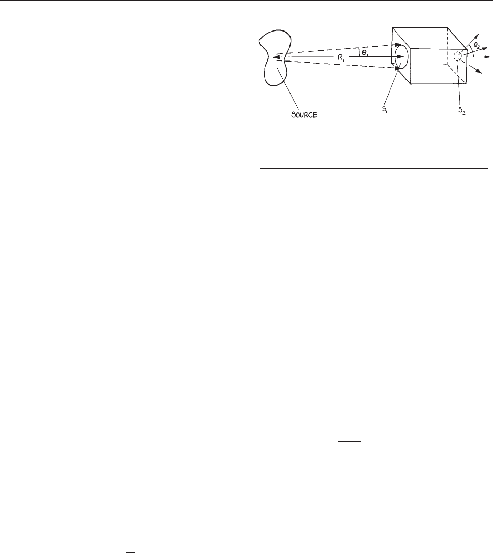
methods of analysis can be illustrated through a discussion
of imaging and nonimaging optical systems.
In any experimental setup that in v olv es the collection of
light from a source and its deli v ery to a light detection sys-
tem, the properties of the optical system between source and
detector should be optimized. This opt imization will take
different forms depending on the application. F or example,
in an experiment in which a weak fluorescent signal from a
liquid in a curvette is to be detected, it is generally the aim to
maximize the amount of collected fluorescence and deli v er
this light to the active surface of the detector. This applica-
tion does not require an imaging optical system, although an
imaging system is often quite satisfactory. On the other
hand, if an image of some object is being delivered to a
CCD camera, then an imaging optical system is required.
4.2.3 Nonimaging Light Collectors
The properties of a nonimaging optical system can be
described schematically with the aid of Figure 4.10. Light
that
enters the front aperture of the system within some
angular range, will leave the system through the exit aper-
ture. In such an arrangement, the brightness of the light
leaving the exit aperture cannot exceed the brightness of
the light entering the entrance aperture. The brightness of
an emitting object is measured in units of Wm
2
per stera-
dian.InFigure 4.10, if the brightness of the radiation
entering
the apertive is B
1
(W m
2
sr
1
) then the power
entering S
1
from the source is:
P
1
¼pB
1
S
1
h
2
1
ð4:60Þ
where the angular range of the enetering rays is h
1
. Assum-
ing that R
1
2
>>S
1
, this angular range is h
1
’ 1=R
ffiffiffiffiffiffiffiffiffiffi
S
1
=p
p
,or
h
2
1
’ S
1
=pR
2
1
. If all the power entering S
1
leaves through
S
2
, then the brightness of the emerging radiation is:
B
2
’
P
1
pS
2
h
2
2
¼
pB
1
S
1
h
2
1
pS
2
h
2
2
ð4:61Þ
where h
2
is the angular spread of emerging rays. So:
B
2
¼
B
1
S
1
h
2
1
S
2
h
2
2
ð4:62Þ
and if B
2
< B
1
,
h
2
ffiffiffiffiffi
S
2
S
1
r
h
1
ð4:63Þ
Practical examples of these devices are given in Section
4.3.3.
4.2.4 Imaging Systems
Generalized Imaging Systems. In a generalized
imaging system, light from an object, located in the
object plane, passes through the system until it reaches
the image plane. In an ideal imaging system all the light
rays that leave a point on the object arrive at a single point
in the imaging plane. Furthermore, the locations of points
in the image plane are such as to preserve the scaling of the
image relative to the object. The image may be magnified
or demagnified, but it should not be distorted.
A type of imaging called aplanatic imaging occurs
when rays parallel to the axis produce a sharp image, inde-
pendent of their distance from the axis. More specifically,
if the angle of an input ray with the axis is h
1
and the output
angle with the axis h
2
, then an aplanatic system satisfies the
sine condition, namely:
sin h
1
sin h
2
¼ constant ð4:64Þ
for rays at all distances from the axis that can pass through the
system. Stigmatic imaging is sharp imaging of a point object
to a point image. An object point that is imaged to an image
point are together called conjugate points.
The Numerical Aperture. If an optical system is
illuminated by a point source on its axis, then the amount
of light collected by the system depends on the angle that
an effective aperture, called the entrance pupil, subtends at
Figure 4.10 Generalized diagram of a nonimaging system.
Light from the source enters the system though the aperture
S
1
over an angular range defined by h
1
and leaves through
aperture S
2
over a range of angles defined by h
2
.
162 OPTICAL SYSTEMS
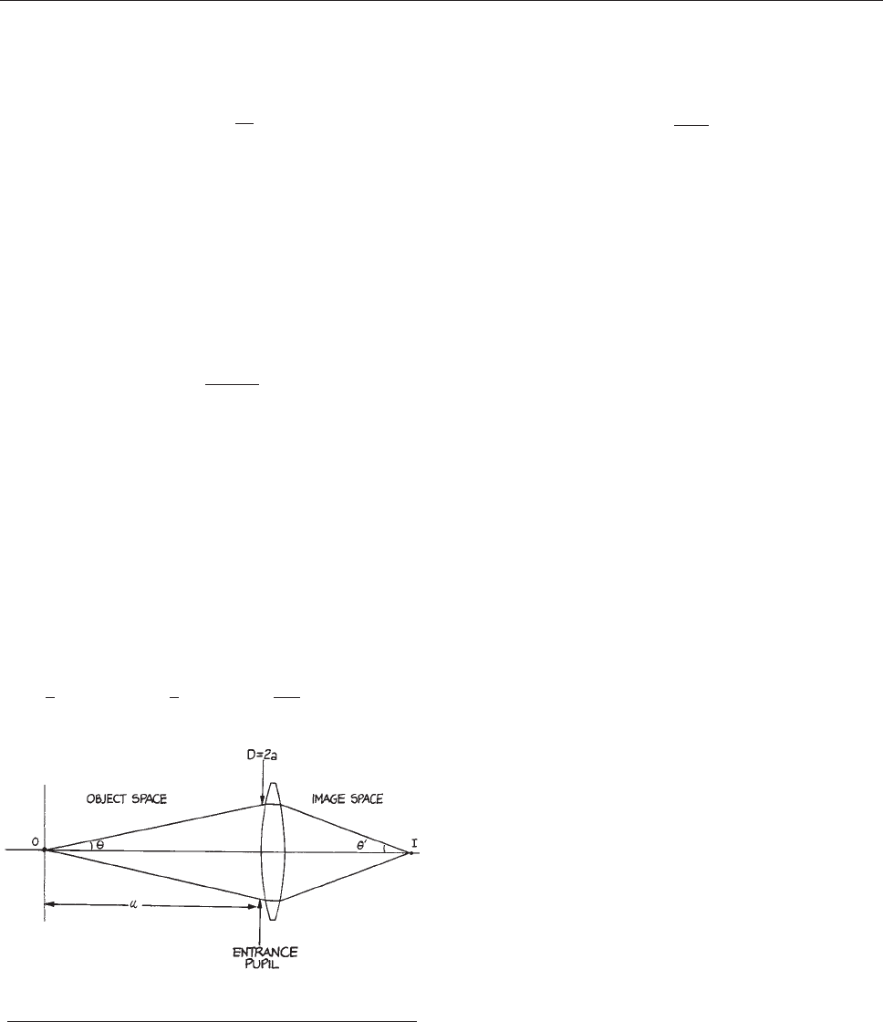
the source. This concept will be discussed further in the
next section. In Figure 4.11 this angle is defined by:
sin h ¼
D
2u
ð4:65Þ
the numerical aperture of the system is:
NA ¼ n sin h ð4:66Þ
where n is the refractive index of the object space (which is
generally 1, but could be higher – for example in micro-
scopy, when an oil-immersion objective lens is used). Now,
a good imaging system obeys the sine condition, which
relates the angles subtended by the exit and entrance pupils
and the magnification m by:
m ¼
n sin h
n
0
sin h
0
ð4:67Þ
where the primed quantities refer to the image space. The
numerical aperture in the image space is:
ðNAÞ
0
¼ n
0
sinh
0
ð4:68Þ
The entrance pupil plays an important geometrical role
in determining the amount of light from an object (or light
source) that can enter and pass through an optical system.
For example, for an entrance pupil diameter (EPD) of D
1
located a distance d
1
from a point source of light, the
fraction of the light emitted by the source that will pass
through the system is:
F¼
1
2
ð1 cos hÞ¼
1
2
1 1 þ
D
2
4d
2
1=2
"#
, ð4:69Þ
where h is the angle shown in Figure 4.11.ForD << d
Equation (4.69) reduces to:
F¼
D
2
16d
2
ð4:70Þ
For a lens, the ratio of focal length to EPD is called the
f/number (f/#) of the lens. An f/1 lens has a ratio of its focal
length to aperture (the open lens diameter) equal to unity. For
a point source at the focal point of such a lens, F¼0 :067.
Apertures, Stops, and Pupils. Apertures controlthe
ray trajectories that can pass through an optical system. The
aperture stop is the aperture within the system that limits
the angular spread, or diameter, of a cone of rays from an
axial point on the object, which can pass through the
system. Another aperture in the system may restrict the
size or angular extent of an object that the system can
image. Awareness of the position and size of these stops
in an optical design is crucial in determining the light-
gathering power of the system, and its ability to deliver
light to an image or detector. The role of the aperture and
field stop can be illustrated with Figure 4.12, which shows a
sin
gle lens being used to image light from a distant object.
The circular aperture behind the lens clearly limits the
diameter of a bundle of rays from an axial point on the
object and is clearly the aperture stop. The second stop,
placed in the image plane, clearly controls the maximum
angle at which rays from off-axis points on the object can
pass through the system. This is the field stop in this case.
Whether a given aperture in an optical system is an aper-
ture stop or a field stop is not always so easy to determine
as was the case in Figure 4.12. Figure 4.13 shows a three-
element
optical system, which actually constitutes what is
called a Gullstrand opthalmoscope
c
. The first lens closest
to the object, called the objective lens, produces a real
inverted image, which is then re-inverted by the erector
lens, to form an image at the focal point of the eyepiece
lens. Aperture A is the aperture stop, and clearly restricts
the angular range of rays from an axial point on the object
that can pass through the system. Aperture B restricts from
what height on the object rays can originate, and still pass
through the system. This aperture is acting as a field stop.
The entrance pupil is the image of the aperture stop
produced by all the elements of the system between the
aperture stop and the object. In Figure 4.13 the two
Figure 4.11 Single lens optical system to illustrate the
concepts of numerical aperture and entrance pupil.
CHARACTERIZATION AND ANALYSIS 163
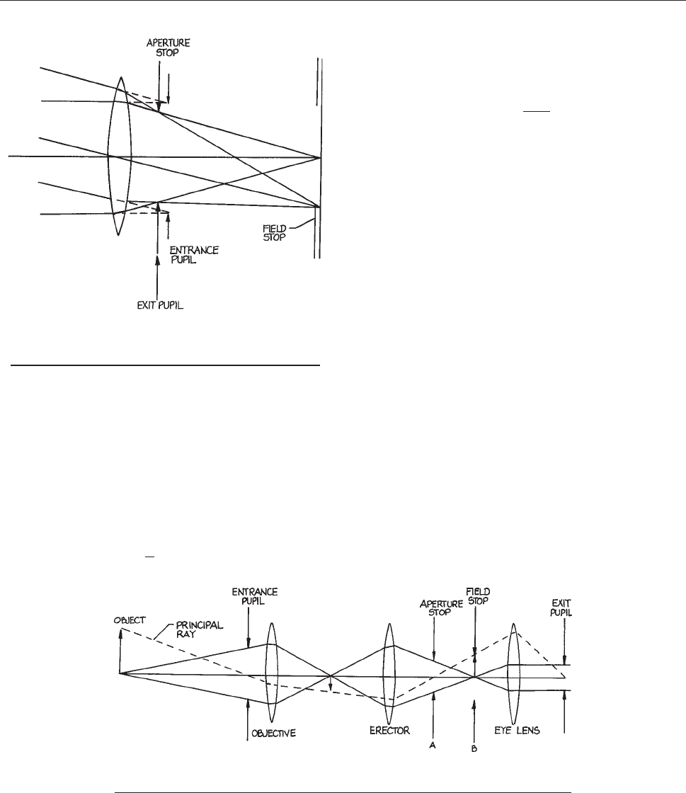
elements producing the image are the erector lens and objec-
tiv e lens. The exit pupil is the image of the aperture stop
produced by all the elements between the aperture stop and
the image, which in Figure 4.13 is just the eye lens. The size
and
location of the entrance and exit pupils determines the
light-gathering and light-delivery properties of the system.
For example, if the entrance pupil has diameter D, and lies a
distance L from a point source of radiant power P (watts)
then the po wer entering the entrance pupil is:
P
1
¼
P
2
ð1 cos hÞ, ð4:71Þ
where tan h ¼ D=2L:
For a point source that is far from the entrance pupil this
result becomes:
P
1
¼
PD
2
1
16L
2
: ð4:72Þ
The solid angle subtended by the entrance pupil in this
case is Dx ¼ D
2
1
=4L
2
.
The light that leaves the system can be characterized by
the total power that leaves the exit pupil, and the angular
range of the rays that leave the exit pupil.
Somewhere in an imaging system there is always an aper-
tur e stop. This may be an actual aperture in an opaque thin
screen placed on the system axis, or it may be the clear
aperture of a lens or mirror in the system. In either case the
aperture stop limits the range of rays that can pass through the
system. This concept is illustrated in Figure 4.14.Arayof
light
such as A, that enters the system and just passes the edge
of the aperture stop, is called a mar ginal ray.AraysuchasB,
that enters the system and passes through the center of the
aperture stop, is called a chief ray . An aperture stop will
always allow some light from every point on an object to
reach the corresponding point on the image. If the amount
of light from the edge of the object (say) that reaches the
corresponding point or the object is sev erely reduced this is
referred to as vignetting.
In Figure 4.13, a ray from an off-axis point on the object
that
passes through the center of the aperture stop is called the
principal ray of the cone of light from the off-axis point.
The ray that enters the system half-way between the high-
est and lowest rays of an oblique beam is called the chief
Figure 4.12 Single lens imaging system to illustrate the
concepts of aperture stop, field stop, and entrance and exit
pupils.
Figure 4.13 Three-lens imaging system showing an aperture stop, a field stop, and
the location of the entrance and exit pupils.
164 OPTICAL SYSTEMS

ray of the beam. In the absence of aberrations, the principal
ray and chief ray are the same, and both pass through the
center of the entrance pupil and aperture stop.
Vignetting. In our previous discussion we have
simplified the actual performance of a real optical system,
because for oblique rays passing through the system the
roles of aperture and field stops become intertwined.
This can be illustrated with Figure 4.15, which shows a
simple
compound lens in which the apertures of the lenses
themselves restrict the rays that can pass through the sys-
tem. A family of oblique rays no longer fills the aperture
stop, because the following lens is acting as a stop. This is
called vignetting. In imaging systems it does not actually
remove points of the object from the image but parts of the
image that depend for their illumination on oblique rays
(especially at large angles) become less bright. Vignetting
is often deliberately allowed to occur in an imaging system
so as to remove certain rays from the system that would
otherwise suffer severe aberration.
Figure 4.14 Aperture stop in front of a single lens showing
vignetting of a family of rays from a distant off-axis point
passing through the lens.
Figure 4.15 Two-lens imaging system showing aperture stop, principal and marginal
rays, and vignetted rays.
CHARACTERIZATION AND ANALYSIS 165
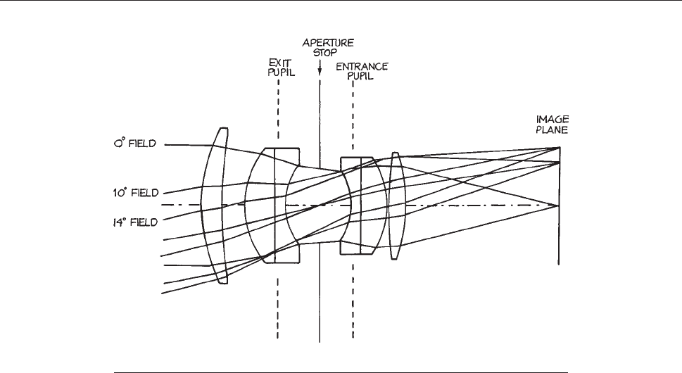
4.2.5 Exact Ray Tracing and Aberrations
If an imaging system is built with a series of lenses and/or
mirrors, then there are inevitably various aberrations. For
refraction at a spherical surface this results because, for
angles of incidence and refraction h
1
, h
2
, respectively,
when light travels from a medium with refractive index
n
1
to one of refractive index n
2
:
n
1
sin h
1
¼n
2
sin h
2
ð4:73Þ
The paraxial approximation, which lacks aberrations,
fails because h
1
6¼ sin h
1
, whereas, in reality, sin h ¼
h h
3
=3! þ h
5
=5! h
7
=7!. The overall effect of aberra-
tions can be greatly reduced, and some types of aberrations
can be eliminated, by using several spherical surfaces, or in
some situations by using an appropriate aspheric surface, a
surface that is not part of a sphere but which is generally
describable in terms of some other conic function or power
series of the coordinates.
Analysis of imaging systems is most conv eniently carried
out using exact ray tracing techniques. In exact ray tracing the
small-angle approximation, Equation (4.8),isnotmadeand
Snell’
s Law is solved e xactly for each ray , at each interface.
By injecting many light rays into the system over some
defining aperture or range of angles the performance of the
system in imaging, focusing, light collection, or light delivery
can be ev aluated precisely. These days this procedure is car-
ried out with optical design software. The most notable soft-
ware packages in this regard are Code V
18
, Zemax
19
,Oslo
20
,
Solstis
21
and Optikwerk
22
. The wide avai lability of these
software tools, and the essentially generic way in which they
are used, makes a brief description of ho w they work and are
used worthwhile. Just as an electronic circuit designer would
be likely to e v aluate a circuit with an analog design tool such
as PSpice, or a digital design tool such as Cadence, Magic, or
Xilinx, an optical designer can ultimately save time, and
avoid mistakes, by numerical simulation of a design.
We will illustrate the use of numerical ray tracing using
the set up procedures appropriate to Code V and with a
specific example: a double Gauss lens used for imaging.
The various optical elements that make up a double Gauss
lens are sho wn in Figure 4.16. For Code V analysis, the axial
position,
curvature, material, and aperture size (radius of
each surface perpendicular to the axis) must be specified
in an optical table showninthiscaseasTable 4.2.Note
the
entries that are specified in each column.
Figure 4.16 Double Gauss lens.
166 OPTICAL SYSTEMS

Table 4.2 Optical table for Code V analysis
Double Gauss – U.S. Patent 2, 532, 751
RDY THI RMD GLA CCY THC GLC
> OBJ: INFINITY INFINITY 100 100
1: 65.81739 8.746658 BSM24_OHARA 0 100
2: 179.17158 9.100796 0 0
3: 36.96542 12.424230 SK1_SCHOTT 0 100
4: INFINITY 3.776966 F15_SCHOTT 100 100
5: 24.34641 15.135377 0 0
STO: INFINITY 12.869768 100 0
7: 27.68891 3.776966 F15_SCHOTT 0 100
8: INFINITY 10.833928 SK16_SCHOTT 100 100
9: 37.46023 0.822290 0 0
10: 156.92645 6.858175 SK16_SCHOTT 0 100
11: 73.91040 63.268743 0 PIM
IMG: INFINITY 0.279291 100 0
SPECIFICATION DATA
EPD 50.00000
DIM MM
WL 656.30 587.60 486.10
REF 2
WTW 1 1 1
XAN 0.00000 0.00000 0.00000
YAN 0.00000 10.00000 14.00000
VUY 0.00000 0.20000 0.40000
VLY 0.00000 0.30000 0.40000
REFRACTIVE INDICES
GLASS CODE 656.30 587.60 486.10
BSM24_OHARA 1.614254 1.617644 1.625478
SK1_SCHOTT 1.606991 1.610248 1.617756
F15_SCHOTT 1.600935 1.605648 1.616951
SK16_SCHOTT 1.617271 1.620408 1.627559
SOLVES
PIM
NO Pickups defined in system
INFINITE CONJUGATES
EFL 99.9866
EFL 63.2687
FFL 17.7398
FNO 1.9997
IMG DIS 62.9895
OAL 84.3452
PARAXIAL IMAGE
HT 24.9295
ANG 14.0000
ENTRANCE PUPIL
DIA 50.0000
THI 68.3242
EXIT PUPIL
DIA 58.0886
THI 52.8928
CHARACTERIZATION AND ANALYSIS 167

With ray tracing software the various parameters of this
lens system can be simultaneously optimized so as to pro-
duce the sharpest possible image of an object.
For the double Gauss lens, for example, th e curvatures
of the various surfaces, their spacings, and the type of
glass used for each element can be simultaneously var-
ied. In pr actice, various constr aints must be included in
this process: lens elements should not be too th ick or too
thin, and the glasses chosen must be available. The var-
iable paramete rs for a glass are its refractive index n and
its dispersion dn/dk, both of which vary with wave-
length.
The dispersion is frequently characterized by the Abbe V
number, which provides a relative measure of dispersion:
V ¼
n
d
1
n
F
n
C
ð4:74Þ
where the refractive index n is specified at the three
wavelengths d (the helium d line at 587.6 nm), F (the
hydrogen F line at 486.1 nm), and C (the hydrogen C line
at 656.3 nm). Some of the standard wavelengths that are
used in optical design are listed in Table 4.3. The different
glasses
that are available from a manufacturer are gener-
ally plotted on a glass chart, which plots (n
d
– 1) against V.
Figure 4.17 shows such a chart for glasses available from
Schott.
Other major suppliers of optical glass are Corning,
Hoya, and Ohara.
Two old classifications of glass into crown and flint
glasses can be related to the glass chart. Crown glasses
are glasses with a V value greater than 55 if n
d
< 1.6 and
V >50ifn
d
> 1.6. The flint glasses have V values below
these limits. The rare-earth glasses contain rare-earths
instead of SiO
2
, which is the primary constituent of crown
and flint glasses.
Spot Diagram. If very many rays are launched from
a point on the objec t so as to cover the e ntrance pupil
of the system, the resulting p attern of ray intersections
with the image plane is called the spot diagram.A
tight spot diagram indicates t hat the effects of several
aberrations, notably spherical, astigmatism, coma, and
curvature of field have been markedly reduced. It must
be remembered that this does not imply that the
aberrations themselves have necessarily been
eliminated, but that their effects have been reduced in
the situation examined. A tighter spot diagram can
always be produced by re ducing th e siz e of the
entrance pupil.
d
Figure 4.18 shows s uch a spot
diagram for a double Gauss lens being operated with a
relatively large entrance pupil.
Chromatic Aberrations. Because, in general, the
index of refraction increases with decreasing wavelength,
the focal length of a singlet lens
e
will, for example, be
shorter for blue light than it is for red light. This effect
leads to imperfect imaging, so that in white light
illumination both axial and off-axis object points will be
imaged, not as bright points, but as regions that show
blurring from red to blue. For axial object points this
blurring is spherically symmetric and results from the
image being closer to the lens for blue light than for red
light. This is simple chromatic aberration. For off-axis
object points, the magnification of the system varies with
wavelength, leading to what is called lateral color or
transverse chromatic aberration.
Table 4.3 Standard wavelengths used in optical design
Wavelength (nm) Designation Source
312.59 mercury
334.15 mercury
365.01 ‘ mercury
404.66 h mercury
435.83 g mercury
479.99 F9 mercury
486.13 F hydrogen
546.07 e mercury
587.56 d helium
589.29 D sodium (doublet)
632.80 He-Ne laser
643.85 c9 cadmium
656.27 c hydrogen
706.52 r helium
852.11 s cesium
1013.98 t mercury
1060.00 neodymium laser
1529.58 mercury
1970.09 mercury
2325.42 mercury
168 OPTICAL SYSTEMS
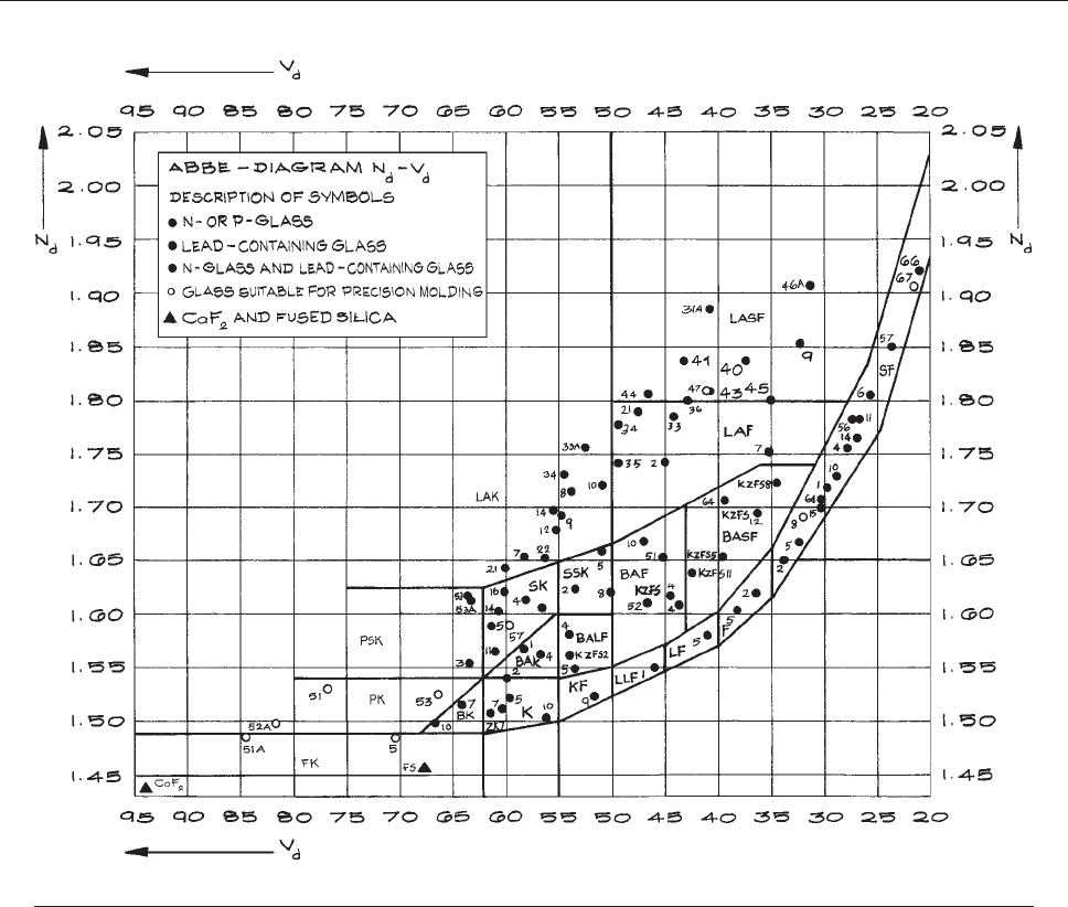
Chromatic aberration can be corrected for two colors
(generally red and blue) and the imaging of axial points.
Such lenses take the form of an achromatic doublet where
a doublet lens is generally fabricated from a positive (con-
verging) crown glass element and a negative (diverging)
flint glass element.
If a compound lens is designed to remove c hromatic
aberration at three wavelengths it is called an apo-
chromat and if correcting for four wavelengths a
supe rachromat.
Achromatic doublets, because they have at least
three spherical surfaces (or four in an air-spaced
achromat), can also better correct for other aberrations
than a singlet lens. Such lenses are available in a
range of apertures an d focal lengths from many manu-
facturers.
Geometrical Aberrations. In a perfect imaging
system, all ra ys from a poin t on the objec t would
pass through an identical point on the image and there
Figure 4.17 The glass chart for glasses available from Schott.
CHARACTERIZATION AND ANALYSIS 169
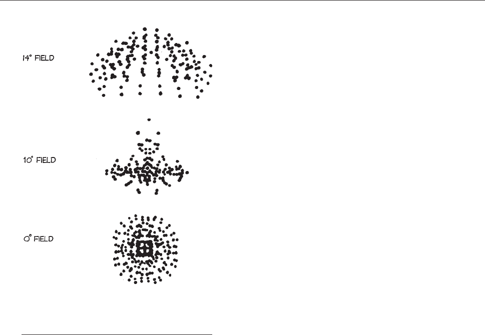
would be a linear relation between the coordina tes of
points on t he image and corresponding points on th e
object.
For an axially symmetric system we can arbitrarily
choose the object point in Figure 4.19 to be at the
(x, y) p oint (0, h) i n the object. We take the polar coor-
dinates of a ray fro m this point to a point P in the
entrance pupil as (q, h). In the general case this ray will
intersect the image plane at point I9 with coordinates in
the image plan e ( x9, y9). The aberrations Dx9, Dy9 are the
displacements of (x9, y9) from the paraxial image point
I(x9
0
, y9
0
) for which there is a linear transformation from
the coordinates of the point on the object. The lowest-
order aberration terms contain terms in either h
3
, h
2
q,or
hq
2
and are referred to as third-order aberrations .
Although there a re differences in terminology concern-
ing these terms in the literature we can write (following
Born and Wolf
11
)
Dy
0
¼ Bq
3
cos h Fhq
2
ð2 þ cos ZhÞ
þð2C þ DÞh
2
q cos h Eh
3
ð4:75Þ
Dx
0
¼ Bq
3
sin h Fhq
2
sin 2h þ Dh
2
q sin h ð4: 76Þ
The coefficients B, C, D, E, and F characterize the five
primary or Seidel aberrations. Their magnitude in any
given optical design can be calculated and visualized with
ray tracing optical software.
Spherical Aberration B 6¼0. When all the
coeffic ients in Equatio ns (4.75) and ( 4.76) are zero
except for B, the remaining effect is spherical
aberration. This aberration is strikingly observed in the
imaging of an axial point source, which will be imaged to
a circular bright region whose radius reveals the extent of
the aberration. For an axial point h ¼ 0 and from
Equations (4.75) and (4.76), Dy9 ¼ Bq
3
cos h, Dx9 ¼
Bq
3
sin h, which can be written as:
Dr ¼ Bq
3
ð4:77Þ
For focusing of parallel light the ‘‘best-form’’ singlet lens for
minimum spherical aberration is close to conv e x-plane (with
the con v ex surface towards the incoming parallel light).
Coma F 6¼ 0. Coma is the aberration in which the image
of an off-axis point varies for rays passing through
different regions of the entrance pupil. It is difficult to
produce a lens where coma alone can be observed. The
spot diagram in Figure 4.18 shows the characteristic
‘‘flaring’’ of the spot pattern, like a comet tail, which
gives the aberration its name. Coma can be controlled by
varying the curvatures of surfaces in the system.
Astigmatism C 6¼ 0. All the aberrations disc ussed so
far are defects in the imaging of meridional rays,thatis,
rays in the plane containing the axis of the lens and the
line from the object point through the center of the lens.
The imaging is different for sagittal rays, that is, ra ys in
the sagittal plane, which is perpendicular to the
meridional plane, as illustrated in Figure 4.20.The
Figure 4.18 Spot diagrams for a double Gauss
lens showing the spot diagrams for families of rays
entering the lens at angles of 0°,10°, and 14° – the
field angles.
170 OPTICAL SYSTEMS
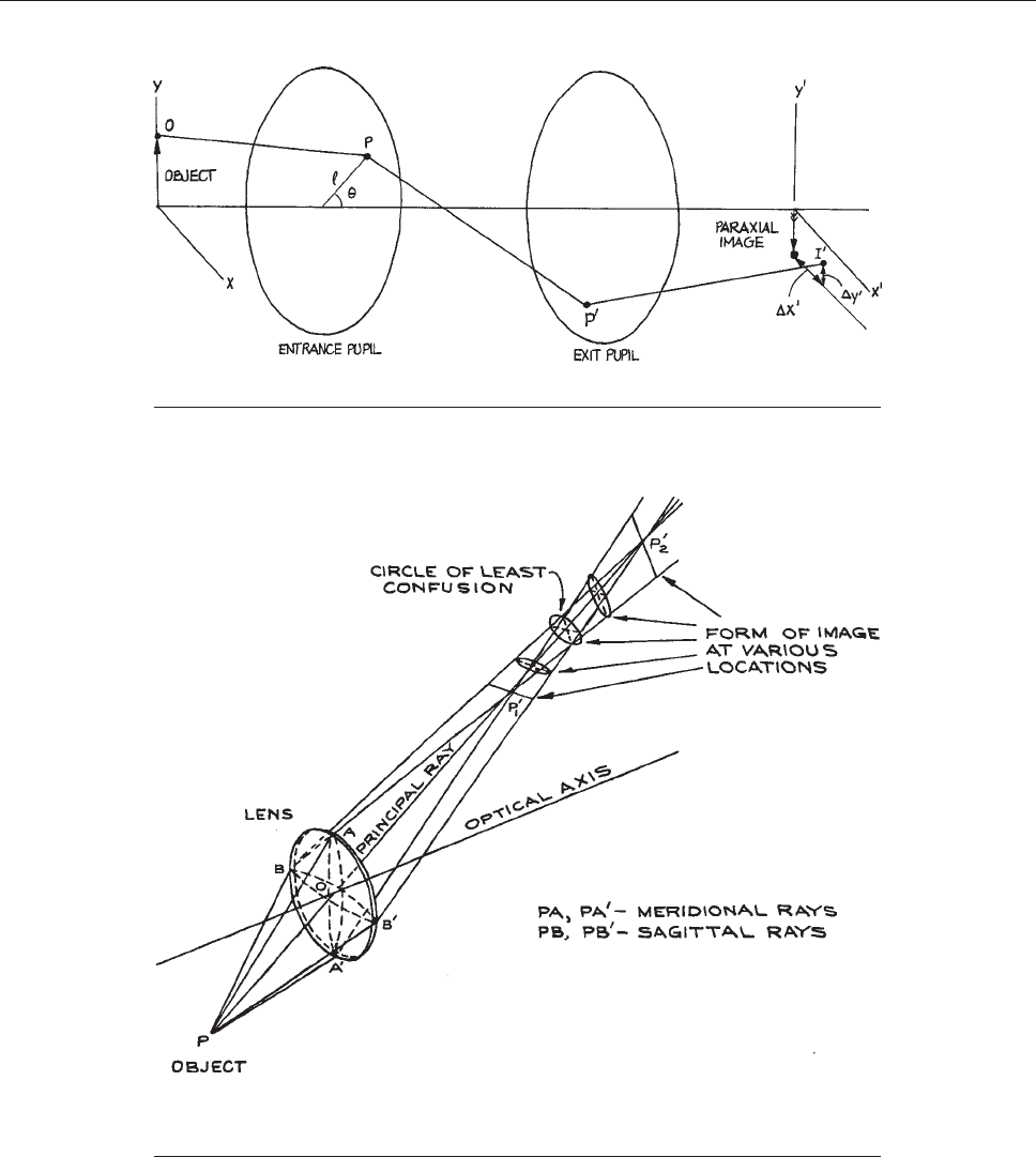
Figure 4.19 Diagram of a generalized imaging system used to discuss aberrations.
Figure 4.20 Illustrating astigmatism. Meridional rays PA and PA9 are imaged at P9
1
, sagittal
rays PB and PB9 are imaged at P9
2
. (After A. C. Hardy and F. H. Perrin, Principles of Optics,
McGraw-Hill, New York, 1932; by permission of McGraw-Hill Book Company, Inc.).
CHARACTERIZATION AND ANALYSIS 171
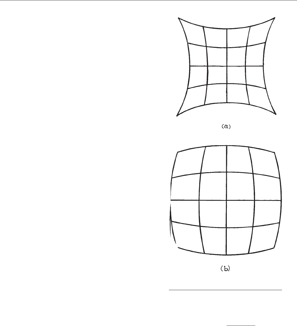
resulting aberration is called astigmatism.Itcanbe
controlled by lens curvature and refractive-index
variations a nd by the use of apertures to restric t the
range of angles and off-axis distances at which rays
can traverse the lens.
Distortion, E 6¼ 0. In distortion, the magnification
varies across the image plane. The height of the image
above the axis relative to the height of the object varies
across the image.
Each object point appear s as a point in the image, and
the images of object points on a plane orthogo nal to the
axis are also on such a plane. The magnification of an
object line segment may, however, vary with its distance
from the axis. This is called dis tortion . It takes two com-
mon fo r ms: pincushion and barrel distortion, as illus-
trated in Figure 4.21. Distortion is sensitive to the lens
shape
and spacing, and to the size and position of aper-
tures in the system – called stops.
For further details of aberrations and how to deal with
them, we refer the reader to specialized texts on optics
(especially lens design), such as those by Born and
Wolf,
11
Ditchburn,
23
Levi,
24
Smith,
25,26
Shannon,
27
and
Laikin.
28
Curvature of Field, D 6¼ 0. In this aberration, the
image of a plane object perpendicular to the axis is sharp
over a curved surface in the image space.
Modulation Transfer Function. A common way of
characterizing the performance of an imaging system is
through its modulation transfer function or MTF. This
refers to the a bility of the system to replicate in the
image, periodic features in the object. An optical test
pattern used to show this consists of a series of white
and black bands. These bands wi ll be smeared out in
the image to a greater or lesser extent be cause of
aberrations, and ultimately, if geometrical aberrations
are absent, by diffraction.
The relative brightness of the object and image will
appear schematically as shown in Figure 4.22.Wecan
chara
cterize the visibility, contrast or modulation of the
image as:
visibility ¼
max min
max þ min
ð4:78Þ
Figure 4.21 (a) ‘‘Pincushion’’ distortion;
(b) ‘‘barrel’’ distortion.
172 OPTICAL SYSTEMS
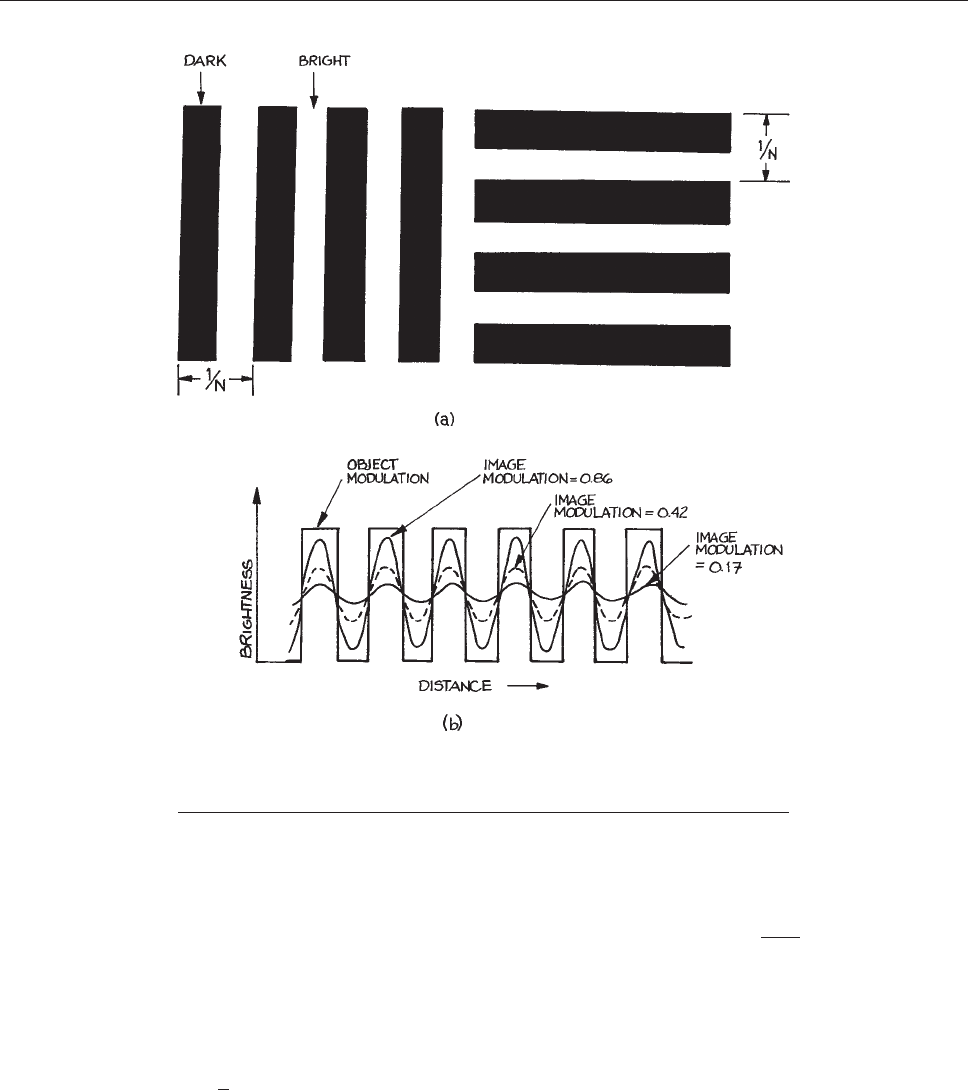
If the visibility is plotted versus the number of lines per
millimeter in the object in this case, this shows the mod-
ulation transfer function. Figure 4.23 shows an example for
the
double Gauss lens system shown in Figure 4.16. The
MTF
is ultimately limited by diffraction. In this case, for a
pattern with m lines per millimeter:
MTFðmÞ¼
1
p
ð2/ sin 2/Þð4:79Þ
where
/ ¼ cos
1
k
0
m
2NA
ð4:80Þ
In Equation (4.80) k
0
is measured in mm and NA is the
numerical aperture of the system.
A quantity, closely related to the MTF, for charactering
MTF, and also the focusing of a light beam, or laser beam,
is the Strehl ratio. The Strehl ratio is the ratio of the
Figure 4.22 (a) An object with sharp contrast between bright and dark bands;
(b) the corresponding image brightness variation for differing degrees of
modulation.
CHARACTERIZATION AND ANALYSIS 173
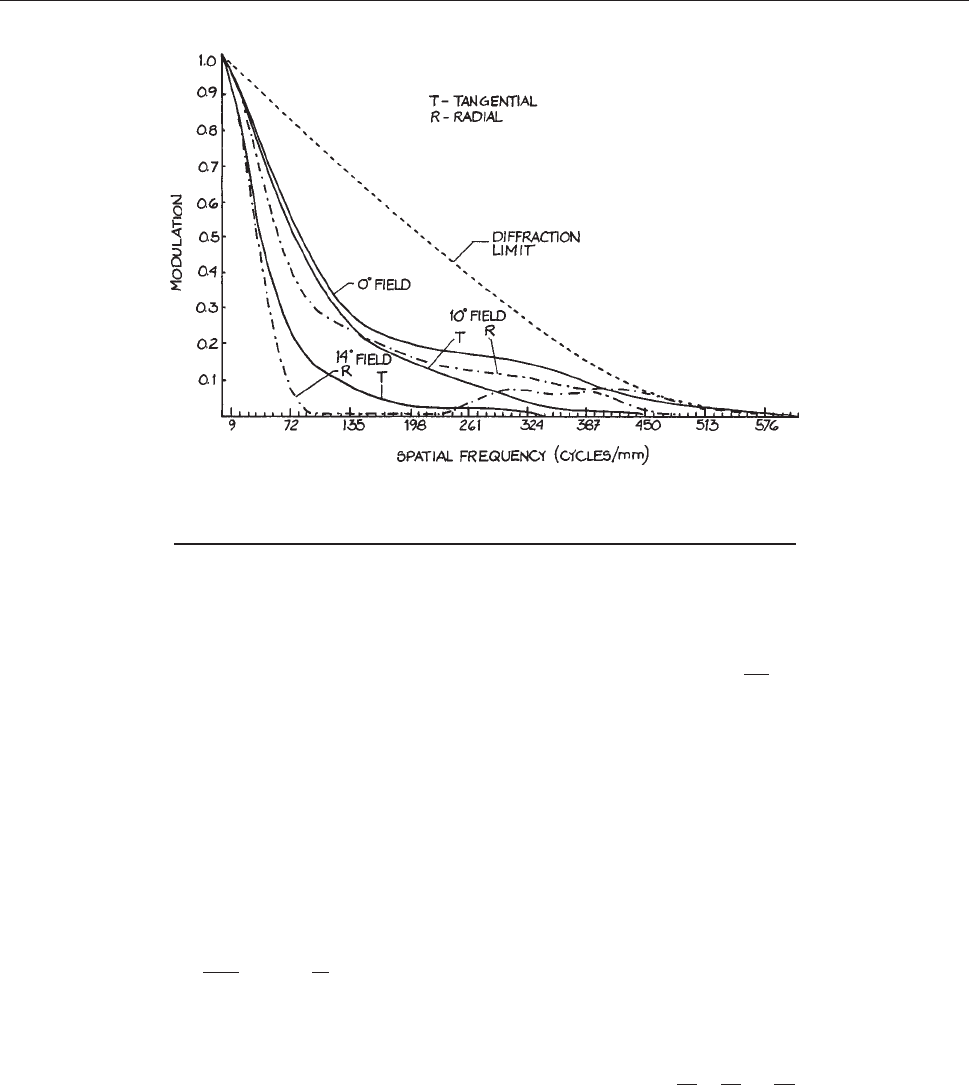
illumination at the center of a focused or circular image to
the illumination of an equivalent unaberrated image. The
interested reader can see a more detailed discussion in
Smith.
25
4.2.6 The Use of Impedances in Optics
The method of impedances is the easiest way to calculate
the fraction of incident intensity transmitted and reflected
in an optical system. It is also the easiest way to follow the
changes in polarization state that result when light passes
through an optical system.
As we have seen in Section 4.1, the impedance of a
plane
wave traveling in a medium of relative permeability
l
r
, and dielectric constant e
r
is:
Z ¼
ffiffiffiffiffiffiffiffiffi
l
r
l
0
e
r
e
0
r
¼ Z
0
ffiffiffiffiffi
l
r
e
r
r
ð4:81Þ
If l
r
¼ 1, as is usually the case for optical media, the
impedance can be written as:
Z ¼ Z
0
=n ð4:82Þ
This impedance relates the transverse E and H fields of the
wave:
Z ¼
E
tr
H
tr
ð4:83Þ
When a plane wave crosses a planar boundary between
two different media, the components of both E and H
parallel to the boundary have to be continuous across that
boundary. Figure 4.24(a) illustrates a plane wave polarized
in
the plane of incidence striking a planar boundary
between two media of refractive indices n
1
and n
2
. In terms
of the magnitudes of the vectors involved:
E
i
cos h
1
þ E
r
cos h
1
¼ E
t
cos h
2
ð4:84Þ
H
i
H
r
¼ H
t
ð4:85Þ
Equation (4.82) can be written as:
E
i
Z
1
E
r
Z
1
¼
E
t
Z
2
ð4:86Þ
Figure 4.23 Modulation transfer function (MTF) for a double Gauss lens.
The MTF for 0°,10°, and 14° fields in both the tangential and radial directions
are shown, and also the diffraction limit of an aberration-free system.
174 OPTICAL SYSTEMS
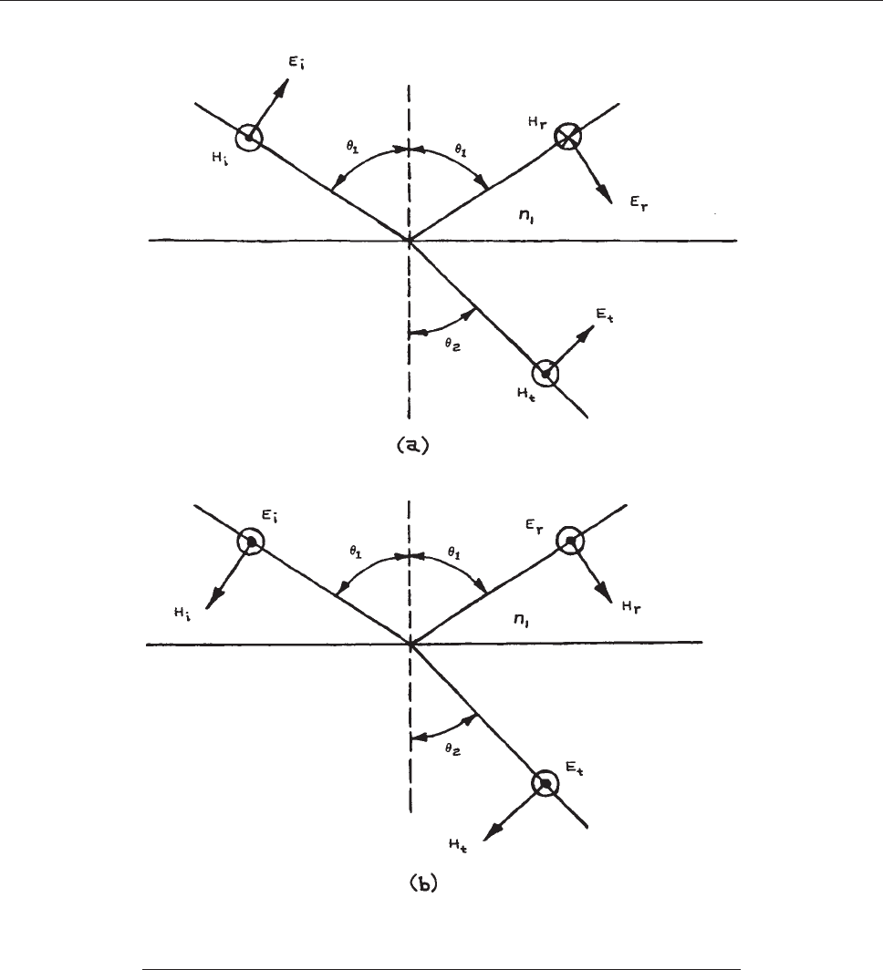
Figure 4.24 Reflection and refraction at a planar boundary between two different
dielectric media: (a) wave polarized in the plane of incidence (P-polarization);
(b) wave polarized perpendicular to the plane of incidence (S-polarization).
CHARACTERIZATION AND ANALYSIS 175
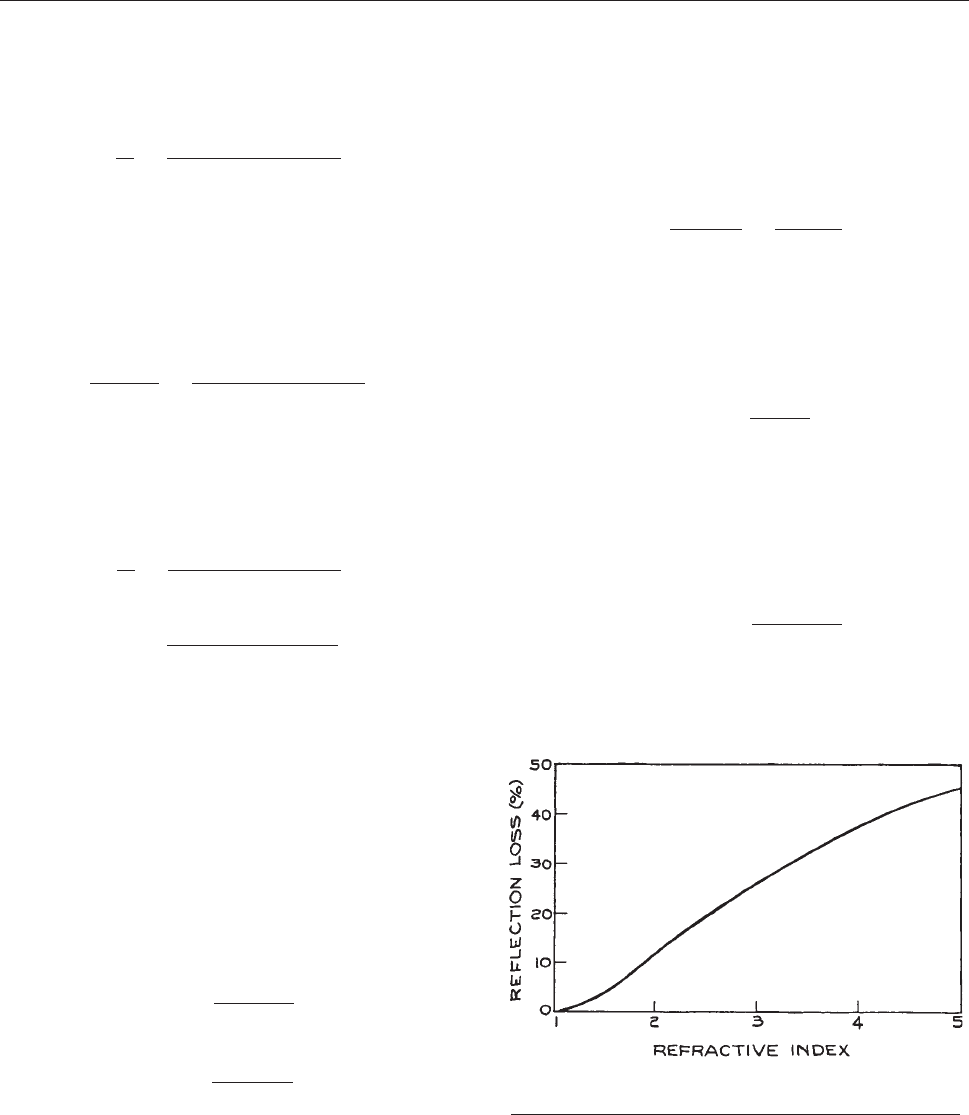
It is easy to eliminate E
t
between Equations (4.84) and
(4.86) to give:
q ¼
E
r
E
i
¼
Z
2
cos h
2
Z
1
cos h
1
Z
2
cos h
2
þ Z
1
cos h
1
ð4:87Þ
where q is the reflection coefficient of the surface. The
fraction of the incident energy reflected from the surface
is called the reflectance, R ¼ q
2
. Similarly, the transmis-
sion coefficient of the boundary is:
s ¼
E
t
cos h
2
E
i
cos h
1
¼
2Z
2
cos h
2
Z
2
cos h
2
þ Z
1
cos h
1
ð4:88Þ
By a similar treatment applied to the geometry shown in
Figure 4.24(b), it can be shown that for a plane wave
polarized
perpendicular to the plane of incidence:
q ¼
E
r
E
i
¼
Z
2
sec h
2
Z
1
sec h
1
Z
2
sec h
2
þ Z
1
cos h
1
ð4:89Þ
s ¼
2Z sec h
2
Z
2
sec h
2
2
þ Z
1
sec h
1
ð4:90Þ
If the effective impedance for a plane wave polarized in
the plane of incidence (P-polarization)
f
and incident on a
boundary at angle h is defined as:
Z
0
¼ Z sec h ð4:91Þ
and for a wave polarized perpendicular to the plane of
incidence (S-polarization)
g
as:
Z
0
¼ Z sec h ð4:92Þ
then a universal pair of formulae for q and s results:
q ¼
Z
0
2
Z
0
1
Z
0
1
þ Z
0
2
ð4:93Þ
s ¼
2Z
0
2
Z
0
1
þ Z
0
2
ð4:94Þ
It will be apparent from an inspection of Figure 4.24 that
Z9 i
s just the ratio of the electric-field component parallel to
the boundary and the magnetic-field component parallel to
the boundary. For reflection from an ideal mirror, Z9
2
¼ 0.
In normal incidence, Equations (4.87) and (4.89)
become
identical and can be written as:
q ¼
Z
2
Z
1
Z
2
þ Z
1
¼
n
1
n
2
n
1
þ n
2
ð4:95Þ
Note that there is a change of phase of p in the reflected
field relative to the incident field when n
2
> n
1
.
Since intensity } (electric field)
2
, the fraction of the
incident energy that is reflected is:
R ¼ q
2
¼
n
1
n
2
n
1
n
2
2
ð4:96Þ
R increases with the index mismatch between the two
media, as shown in Figure 4.25. If there is no absorption
of
energy at the boundary, the fraction of energy trans-
mitted, called the transmittance,is
T ¼ 1 R ¼
4n
1
n
2
ðn
1
þ n
2
Þ
2
ð4:97Þ
Note that because the media on the two sides of the
boundary are different, T 6¼ | s |
2
.
Figure 4.25 Reflection loss per surface for normal inci-
dence as a function of refractive index.
176 OPTICAL SYSTEMS

Reflectance for Waves Incident on an
Interface at Oblique Angles.
If the wave is not
incident normally, it must be decomposed into two
linearly polarized components, one polarized in the plane
of incidence, and the other polarized perpendicular to the
plane of incidence.
For example, consider a plane-polarized wave incident on
an air glass (n ¼ 1.5) interface at an angle of incidence of
30°, with a polarization state exactly intermediate between
the S-polarization and the P-polarization. The angle of
refraction at the boundary is found from Snell’s law:
sin h
2
¼
sin 308
1:5
ð4:98Þ
and so h
2
¼ 19.47°.
The effective impedance of the P-component in the air
is:
Z
0
P1
¼ 376:7 cos h
1
¼ 326:23 X ð4:99Þ
and in the glass:
Z
0
P2
¼
376:7
1:5
cos h
2
¼ 236:77X ð4:100Þ
Thus, from Equation (4.87), the reflection coefficient for
the P-component
is:
q
P
¼
236:77 326:33
236:77 þ 326:23
¼0:159 ð4:101Þ
The fraction of the intensity associated with the P-compo-
nent that is reflected is q
P
2
¼ 0.0253.
For the S-component of the input wave:
Z
0
S1
¼
376:7
cos h
1
¼ 434:98X ð4:102Þ
Z
0
S2
¼
376:7
1:5 cos h
2
¼ 266:37X
q
S
¼
266:37 434:98
266:37 þ 434:98
¼0:240
ð4:103Þ
The fraction of the intensity associated with the S-
polarization component that is reflected is q
S
2
¼
0.0578. Sin ce the input wave conta ins equ al amo unts
of S-andP-polarization, the overall reflectance in this
case is:
R ¼ <q
2
>
av
¼ 0:0416 ’ 4% ð4:104Þ
Note that the reflected wave now contains more S-
polarization than P, so the polarization state of the
reflected wave has been changed – a phenomenon that
will be discussed further in Section 4.3.6.
Brewster’s Angle. Returning to Equation (4.87),it
might be asked whether the reflectance is ever zero. It is
clear that q will be zero if:
n
1
cos h
2
¼ n
2
cos h
1
ð4:105Þ
which, from Snell’s law [Equation (4.6)], gives:
cos h
1
¼
n
1
n
2
ffiffiffiffiffiffiffiffiffiffiffiffiffiffiffiffiffiffiffiffiffiffiffiffiffiffiffiffiffiffiffiffiffiffiffi
1
n
1
n
2
2
sin
2
h
1
s
ð4:106Þ
giving the solution:
h
1
¼ h
B
¼ arcsin
ffiffiffiffiffiffiffiffiffiffiffiffiffiffiffiffiffi
n
2
2
n
2
1
þ n
2
2
s
¼ arctan
n
2
n
1
ð4:107Þ
The angle h
B
is called Brewster’s angle. A wave polar-
ized in the plane of incidence and incident on a boundary at
this angle is totally transmitted. This allows the design of
low-reflection-loss windows in laser systems, as will be
seen in Section 4.6.2.IfEquation (4.89) is inspected care-
fully
, it will be seen that there is no angle of incidence that
yields zero reflection for a wave polarized perpendicular to
the plane of incidence.
Transformation of Impedance through
Multilayer Optical Systems.
The impedance
concept allows the reflection and transmission
characteristics of multilayer optical systems to be
evaluated very simply. If the incident light is incoherent
(a concept discussed in more detail later in Section 4.5.1),
then
the overall transmission of a multilayer structure
is just the product of the transmittances of its various
interfaces. For example, an air–glass interface transmits
CHARACTERIZATION AND ANALYSIS 177
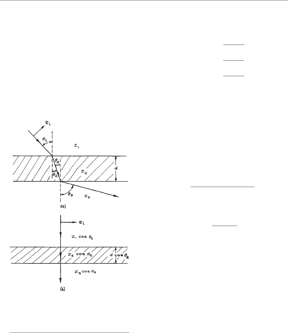
about 96% of the light in normal incidence. The
transmittance of a parallel-sided slab is 0.96 3 0.96 ¼
92%. This simple result ignores the possibility of
interference effects between reflected and transmitted
waves at the two faces of the slab. If the faces of the
slab are very flat and parallel, and if the light is
coherent, such effects cannot be ignored. In this case, the
method of transformed impedances is useful.
Consider the three-layer structure shown in Figure
4.26(a). The path of a ray of light through the structure
is shown. The angles h
1
, h
2
, and h
3
can be calculated from
Snell’s law. As an example, consider a wave polarized in
the plane of incidence. The effective impedances of media
1, 2, and 3 are
Z
0
1
¼ Z
1
cos h
1
¼
Z
0
cos h
1
n
1
Z
0
2
¼ Z
2
cos h
2
¼
Z
0
cos h
2
n
2
Z
0
3
¼ Z
3
cos h
3
¼
Z
0
cos h
3
n
3
ð4:108Þ
It can be shown that the reflection coefficient of the
structure is exactly the same as for the equivalent structure
in Figure 4.26(b) in normal incidence, where the effective
thickness of layer 2 is now:
d
0
¼ d cos h
2
ð4:109Þ
The reflection coefficient of the structure can be calcu-
lated from its equivalent structure using the transformed
impedance concept.
15,29
The transformed impedance of medium 3 at the boun-
dary between media 1 and 2 is:
Z
00
3
¼ Z
0
2
Z
0
3
cos k
2
d
0
þ iZ
0
2
sin k
2
d
0
Z
0
2
cos k
2
d
0
þ iZ
0
3
sin k
2
d
0
ð4:110Þ
where k
2
¼ 2p/k
2
¼ 2pn
2
/k
0
. The reflection coefficient of
the whole structure is now just:
q ¼
Z
00
3
Z
0
1
Z
00
3
þ Z
0
1
ð4:111Þ
the reflectance of the whole structure is R ¼ |q|
2
, and its
transmittance is:
T ¼ 1 R ð4:112Þ
In a structure with more layers, the transformed impe-
dance formula [Equation (4.108)] can be used sequentially,
starting at the last optical surface and working back to
the first. More examples of the use of the technique of
transformation of impedance will be given in Sections
4.3.1 and 4.3.7.
Optical System Design Software. As well as the
ray tracing optical design programs mentioned earlier, such
as Code V, there is a broad range of other software available
Figure 4.26 (a) Wave polarized in the plane of
incidence passing through a dielectric slab of
thickness d and impedance Z
2
separating two semi-
infinite media of impedances Z
1
and Z
3
, respectively;
(b) equivalent structure for normal incidence.
178 OPTICAL SYSTEMS

commercially for optical system design including: laser
system design (GLAD, PARAXIA, ASC, and LASFIT);
atmospheric optical properties and sensors (ONTAR);
optical system solid modeling (LightTools, TracePro);
projection systems, fiber optics, and complex sources
(ASAP); beam propagation for integrated and fiber optics
(BeamProp); vector diffraction grating analysis software
and simulation (GSOLVER); optical thin-film and coating
design, material analysis, ellipsometry, spectrophotometry
and thin-film metrology; [Film Wizard, FilmSpectrum,
TFCalc, Thin Film Design Package (Thin Film Center)];
and analysis of laser beam propagation (FRESNEL).
4.2.7 Gaussian Beams
Gaussian beams are propagating-wave solutions of Max-
well’s equations that are restricted in lateral extent even in
free space. They do not need any beam-confining reflective
planes, as do the confined electromagnetic-field modes of
waveguides.
29
Lasers frequently emit narrow beams of light
that are very close in character to ideal Gaussian beams.
The field components of a plane transverse electromag-
netic wave of angular frequency x propagating in the
z-direction are of the form:
V ¼ V
0
e
iðxtkzÞ
ð4:113Þ
where V
0
is a constant. A Gaussian beam is of the form:
V ¼ Wðx, y, zÞ e
iðxtkzÞ
¼ Uðx, y , zÞe
ixt
ð4:114Þ
where, for example, for a particular value of z, W(x, y, z)
gives the spatial variation of the fields in the xy plane.
W
W gives the relative intensity distribution in the plane;
for a Gaussian beam this gives a localized intensity pattern.
The various Gaussian-beam solutions of Maxwell’s equa-
tions are denoted as TEM
mn
modes; a detailed discussion
of their properties is given by Kogelnik and Li.
16
The out-
put beam from an ideal laser is generally a TEM mode or a
combination of TEM modes. Many laser systems operate
in the fundamental Gaussian mode, denoted TEM
00
. This
is the only mode that will be considered in detail here.
For the TEM
00
mode, W(x, y, z) has the form:
Wðx,y,zÞ¼exp iPðzÞþ
kr
2
2qðzÞ
ð4:115Þ
where P(z)isaphase factor, q(z) is called the beam param-
eter, k equals 2p/k, and r
2
equals x
2
+ y
2
. The beam param-
eter, q(z), is usually written in terms of the phase-front
curvature of the beam R(z), and its spot size, w(z), as:
1
q
¼
1
R
ik
pw
2
ð4:116Þ
q and P obey the following relations:
dq
dz
¼ 1 ð4:117Þ
dP
dz
¼
i
q
ð4:118Þ
For a particular value of z, the intensity variation in the
xy plane (the mode pattern) is, from Equation (4.115):
W
W ¼ exp
ikr
2
2
1
qðzÞ
1
q
ðzÞ
ð4:119Þ
which, from Equation (4.116) gives:
W
W ¼ e
2r
2
=x
2
ð4:120Þ
Thus, w(z) is the distance from the axis of the beam (x ¼
y ¼ 0) where the intensity has fallen to 1/e
2
of its axial
value and the fields to 1/e of their axial magnitude. The
radial distribution of both intensity and field strength of
the TEM
00
mode is Gaussian, as shown in Figure 4.27.
Clearly, from Equation (4.117):
q ¼ q
0
þ z ð4:121Þ
where q
0
is the value of the beam parameter at z ¼ 0. From
Equation (4.118):
PðzÞ¼
ilnq þ constant
¼ilnðq
0
þ zÞþconstant ð4:122Þ
Writing the constant in Equation (4.122) as h þ il
nq
0
,
the full spatial variation of the Gaussian beam is:
U ¼ exp i kz iln 1 þ
z
q
0
þ h
þ
kr
2
2
1
RðzÞ
ik
pw
2
ð4:123Þ
CHARACTERIZATION AND ANALYSIS 179
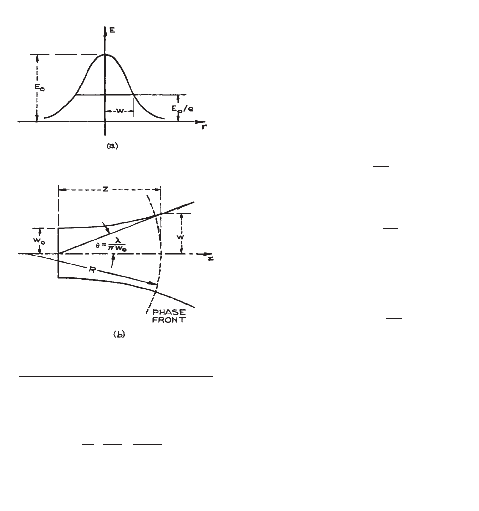
The phase angle h is usually set equal to zero. In the plane
z ¼ 0:
U ¼ exp i
kr
2
2
1
Rð0Þ
ik
pwð0Þ
2
!()
ð4:124Þ
The surface of constant phase at this point is defined by the
equation:
kr
2
2Rð0Þ
¼ constant ð4:125Þ
If the constant is taken to be zero and R(0) infinite, then r
becomes indeterminate and the surface of constant phase is
the plane z ¼ 0. In this case, w(0) can have its minimum
value anywhere. This minimum value is called the mini-
mum spot size w
0
, and the plane z ¼ 0 is called the beam
waist. At the beam waist:
1
q
0
¼
ik
pw
2
0
ð4:126Þ
Using Equations (4.116) and (4.121), for any arbitrary
v
alue of z:
w
2
ðzÞ¼w
2
0
1 þ
kz
pw
2
0
2
"#
ð4:127Þ
The radius of curvature of the phase front at this point is:
RðzÞ¼z 1 þ
pw
2
0
kz
2
"#
ð4:128Þ
From Equation (4.127) it can be seen that the Gaussian
be
am expands in both the positive and negative z-directions
from its beam waist along a hyperbola that has asymptotes
inclined to the axis at an angle:
h
beam
¼ arctan
k
pw
0
ð4:129Þ
as illustrated in Figure 4.27(b). The surfaces of constant
phase
of the Gaussian beam are, in reality, parabolic. For
r
2
<< z
2
(which is generally true, except close to the beam
waist), they are spherical surfaces with the radius of cur-
vature R(z). Although they will not be discussed further
here, the higher-order Gaussian beams, denoted TEM
mn
,
are also characterized by spot sizes and radii of curvature
that are identical to those of the TEM
00
mode and obey
Equations (4.127) and (4.128).
Focusing a Laser beam with a Lens. A lens can
be used to focus a laser beam to a small spot, or systems of
lenses may be used to expand the beam and recollimate it
(i.e., minimize the beam divergence). In such an
application a thin lens will not alter the transverse
intensity pattern of the beam at the lens, but it will alter
its radius of curvature. Far enough from the beam waist,
the radius of curvature of a Gaussian beam behaves exactly
Figure 4.27 (a) Radial amplitude variation of the
TEM
00
Gaussian beam; (b) contour of a Gaussian
beam.
180 OPTICAL SYSTEMS
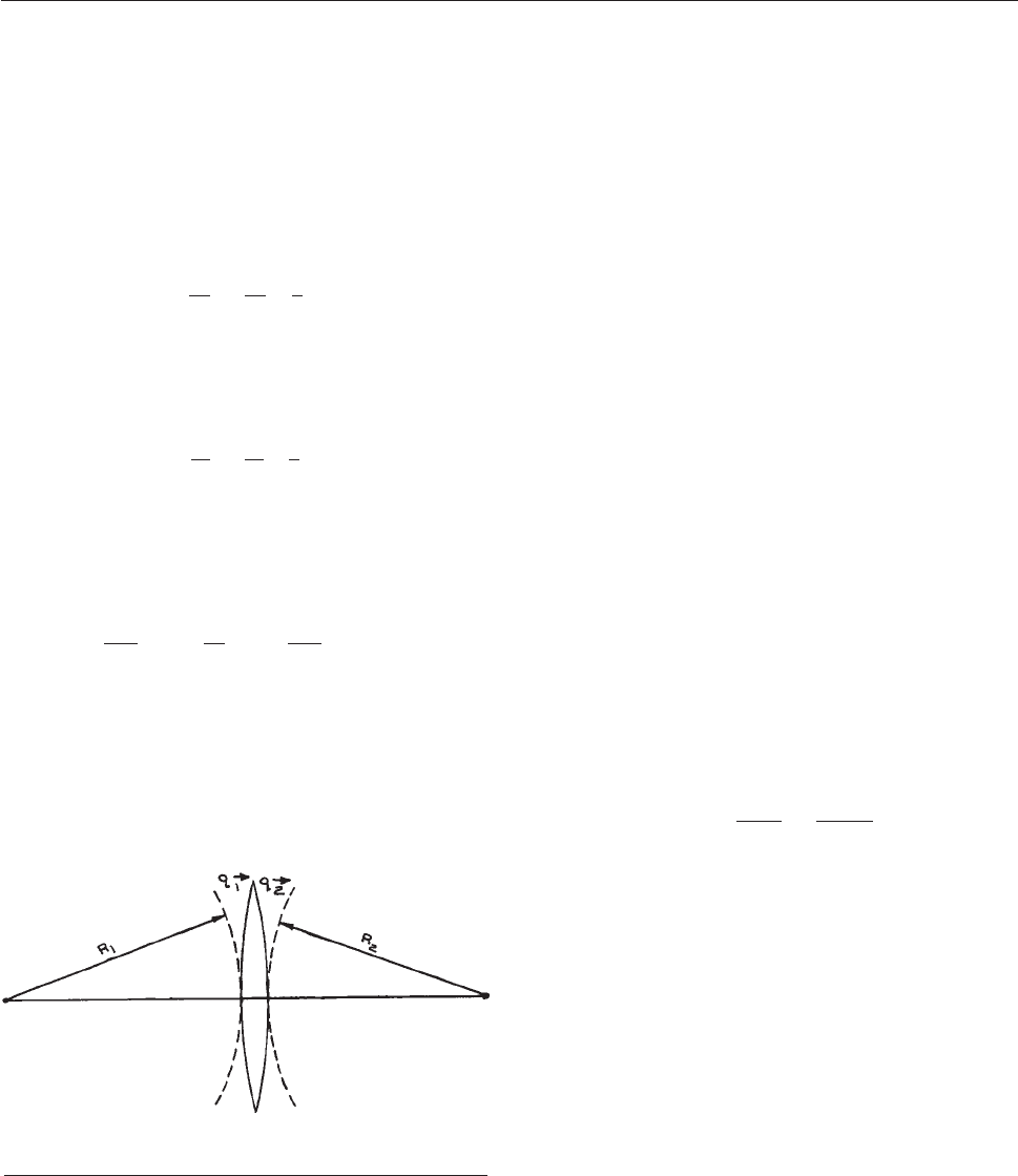
as a true spherical wave, since, for z >> px
2
0
=k, Equation
(4.128) becomes:
RðzÞ¼z ð4:130Þ
No
w, when a spherical wave of radius R
1
strikes a thin
lens, the object distance is clearly also R
1
– the distance to the
point of origin of the wave. Therefore, the radius of curvature
R
2
immediately after passage through the lens must obey:
1
R
2
¼
1
R
1
1
f
ð4:131Þ
as shown in Figure 4.28. Thus, if w is
unchanged at the
lens, the beam parameter after passage through the lens
obeys
1
q
2
¼
1
q
1
1
f
ð4:132Þ
It is straightforward to use this result in conjunction with
Equations (4.116) and (4.121) to give the minimum spot
size w
f
of a TEM
00
Gaussian beam focused by a lens as:
w
f
¼
f k
pw
1
1
f
R
1
2
þ
kf
pw
2
1
2
"#
1=2
ð4:133Þ
where w
1
and R
1
are the laser-beam spot size and radius of
curvature at the input face of the lens. If the lens is placed
very close to the waist of the beam being focused, Equation
(4.133) reduces to:
x
f
¼ f h
B
ð4:134Þ
where h
B
is the beam divergence at the input face of the
lens. If h
B
is a small angle, then w
f
is located almost at the
focal point of the l ens – in reality very slightly closer to
the lens. It is worthwhile comparing the result given b y
Equation (4.134) with the result obtained for a plane wave
b
eing foc us ed by a le ns. In the latter case, the lens diam-
eter D is the factor that limits the lateral extent of the
wave being focused. Diffraction theory
11,23
shows that,
in this case, 84% of the energy is focused into a region of
diameter:
S ¼ 2:44kf =D ð4:135Þ
This is the diameter of the focused Airy disk diffraction
pattern of the lens aperture.
It should be noted that the spot size to which a laser
beam can be focused cannot be reduced without limit
merely by reducing the focal length of the focusing lens.
In the limit the lens becomes a sphere and, of course, is
then no longer a thin lens. In practice, to focus a laser beam
to a small spot, the value of h
B
should be first reduced by
expanding the beam and then recollimating it – generally
with a Galilean telescope, as will be seen in Section 4.3.3.
T
o prevent diffraction effects, the lens aperture should be
larger than the spot size at the lens: D ¼ 2.8w is a common
size used. In this case, if the focusing lens is placed at
the beam waist of the collimated beam, the focal-spot
diameter is:
2w
f
¼
5:6kf
pD
¼
1:78kf
D
ð4:136Þ
In practice, it is difficult to manufacture spherical lenses
with very small values of f / D (called the f /# or f/ nu m-
ber) and at the same time achieve the diffraction-limited
performance pr edicted by this equation. Commer cially
available spherical lenses
30
achieve va lues of 2w
f
of
about 10k. Smaller spot sizes are possible with aspheric
lenses.
The Beam Parameter M
2
. Real laser beams are
often characterized by their M
2
parameter or focusability
parameter. Because of deviations from perfect Gaussian
behavior, whan a real laser beam is focused by an ideal
Figure 4.28 Transformation of a Gaussian beam by a thin
lens.
CHARACTERIZATION AND ANALYSIS 181
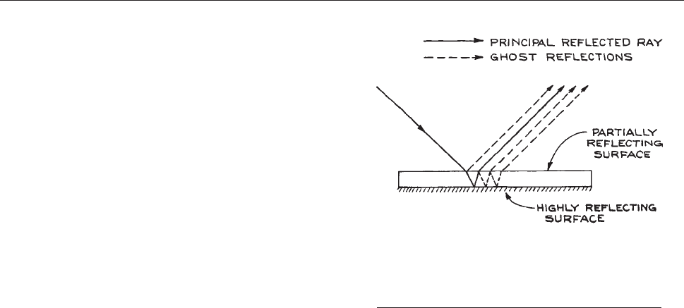
lens placed at the beam waist the focused spotsize is not
w
f
¼ fh
B
, as predicted by Equation (4.134), but is instead:
x
fr
¼ M
2
f h
B
ð4:137Þ
For asymmetrical laser beams there will be two beam
parameters M
2
x
amd M
2
y
for the two lateral coordinates of
the laser beam. The M
2
parameter cannot be measured
from a single measurement of the laser beam. A series of
measurements on a focused beam are made, such as the
position of the focus relative to the focal length of the lens,
the new beam divergence angle after the focus,
the spotsize(s) at the focal point of the lens, and the new
minimum spotsize(s). Commercial instruments that meas-
ure M
2
are available from Coherent, Photon, Inc., and
Spiricon. Here, and wherever suppliers are mentioned in
the text, the list is intended to be representativ e, but not
necessarily exhaustive.
4.3 OPTICAL COMPONENTS
4.3.1 Mirrors
When light passes from one medium to another of different
refractiv e index, there is some reflection, so the interface acts
as a partially reflecting mirror . By applying an appropriate
single-layer or multilayer coating to the interface between
the two media, the reflection can be controlled so that the
reflectance has any desired value between 0 and 1. Both flat
and spherical mirrors made in this way are available – there
are numerous suppliers.
31
If no transmitted light is required,
high-reflectance mirrors can be made from metal-coated
substrates or from metals themselves. Mirrors that reflect
and transmit roughly equal amounts of incident light are
oftenreferredtoasbeamsplitters.
Flat Mirrors. Flat mirrors are used to d eviate the path
of light ra ys w ithout any focusing. The se mirrors can
have their reflective surface on the front face of any
suitable substrate, or on the rear face of a transparent
substrate. Front-surface, totally reflecting mirrors have
the advantage of producing no unwanted additional or
ghost refle ctions; however, their reflective su rfac e is
exposed. Rear-surface mirrors produce ghost reflections,
as illustrated in Figure 4.29, unless their front surface is
antir
eflection coate d; but the reflect ive surface is
protected. Most household mirrors are made this way.
The cost of flat mirrors depends on their size and on the
degree of flatness required.
Mirrors for high-precision applications – for example,
in visible lasers – are normally spec ified to be flat
between k/10 and k/20 f or visible light. This degree of
flatness is not required when the mirror is merely for light
collection and redirection, for example to reflect light
onto the surface of a detector. Mirrors for this sort of
application are routinely flat to within a few wavelengths
of visible light. Excellent mirrors for this purpose can be
made from ‘‘float’’ plate glass,
32
whichisflatto1or2
wavelengths per inch.
New superpolishing techniques have allowed the pro-
duction of super mirrors, which have surf ace roughness
down to 0.1nm or below and loss (absorption plus scat-
tering) below 10
–6
per reflection. Super mirrors allow
the construction of optical resonators with very high Q
values, up to 1 million, for applications such as cavity
ring d own spectroscopy and high finesse interferometry
(see Section 4.7.4). Such mirrors are available from
Lo
s Gatos Researc h, Newport Corporation, an d the
Optical Corporation. More discussion of the issues
involved in fabricating such mirrors is available in
references 34–37.
Figure 4.29 Production of ghost reflections
by a rear-surface mirror whose front surface is
not antireflection coated.
182 OPTICAL SYSTEMS
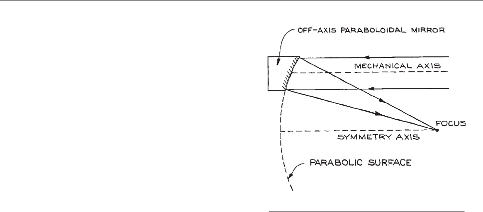
Spherical Mirrors. Spherical mirrors are widely used
in laser construction, where the radii of curvature are
typically rather long – frequently 20 m radius or mor e.
They can be used whenever light must be collected and
focused; however, spherical mirrors are only good for
focusing nearly parallel beams of light that str ike the
mirror close to normal. In common with spherical
lenses, spherical mirrors suffer from various imaging
defects called aberrations, which have been discussed in
Section 4.2.5. A parallel beam of light
that strikes a
spherical mirror far from normal is not focused to a
small spot. When used this way the mirror is
astigmatic, that is, off-axis rays are focused at different
distances in the horizontal and vertical planes. This leads
to blurring of the i mage, or at best the focusing of a point
source into a line image.
A useful practical way to distinguish between a flat
mirror and one with a large radius of curvat ure is to use
the mirror to view a sharp object in grazing incidence.
A cur ved mirror surface will reveal itself through the blur-
ring of the image, while a flat mirror will give a sharp
image.
Paraboloidal and Ellipsoidal Mirrors. Paraboloidal
mirr ors will produce a parallel beam of light when a point
source is placed at the focus of the paraboloidal surface.
Thus, these mirrors are very useful in projection
systems. They are usually made of polished metal,
although versions using Pyrex sub strates are also
available. An important application of parabolic
mirrors is in the off-axis focusing of laser beams,
using off-axis mirrors in which the axis of the
paraboloid does not pass through the mirror. When
they are used in this way there is complete acces s to
the focal region withou t any sha dowing, as shown in
Figure 4.30. Spherical mirrors, on the other hand, do
not
focus well if they are used in this way. Off-axis
paraboloidal mirrors, as well as metal axial
paraboloidal mirrors, are available from Edmund
Optics, II-VI Infrared, Kugler, Lightwave Enterprises,
Melles Griot, Newport, Opti-Forms, OptoSigma, Space
Optics Research Lab, and Thorlabs.
Ellipsoidal mirrors are also used for light collecting.
Light that passes through one focus of the ellipsoid will,
after reflection, also pass through the other. These mirrors,
like all-metal paraboloidal mirrors, are generally made by
electroforming. The surface finish obtained in this way is
quite good, although not so good as can be obtained by
optical polishing. Rhodium-plated electroformed ellipsoi-
dal mirrors are available from Edmund Optics, Melles
Griot, Opti-Forms, and Spectrum Scientific.
Dielectric Coatings. Several dif ferent kinds of single-
layer and multilayer dielectric coatings are available
commercially on the surface of optical components. These
coatings can either reduce the reflectance or enhance it in
some spectral region.
(i) Single-layer antireflection coatings. The mode of
operation of a single-layer antireflection (AR) coating
can be conveniently illustrated by the method of trans-
formed impedances. Suppose medium 3 in Figure
4.31(a) is the surface to be AR coated. Apply to the surface
a
coating with an effective thickness:
d
0
¼ k
2
=4 ð4:138Þ
where k
2
¼ c
0
/mn
2
. The actual thickness of layer 2 is:
d ¼ d
0
= cos h
2
ð4:139Þ
Figure 4.30 Off-axis paraboloidal mirror.
OPTICAL COMPONENTS 183
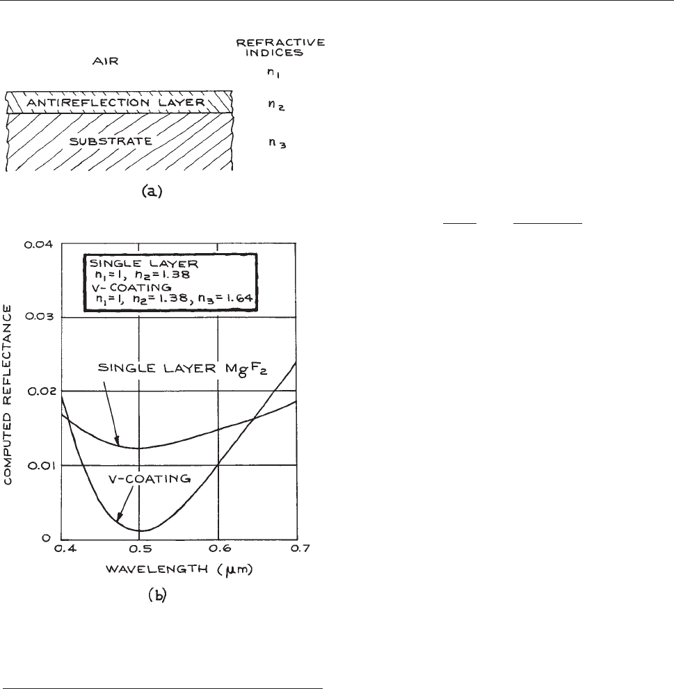
The transformed impedance of medium 3 at the first inter-
face is found by substitution in Equation (4.110):
Z
00
3
¼ Z
0
2
2
=Z
0
3
ð4:140Þ
To reduce the reflection coefficient to zero, we need
Z$
3
¼ Z9
1
; so the effective impedance of the antireflection
layer must be:
Z
0
2
¼
ffiffiffiffiffiffiffiffiffiffiffiffiffi
Z
0
1
Z
0
3
p
ð4:141Þ
Thus, to eliminate reflection of waves linearly polarized
in the plane of incidence and incident at angle h
1
, n
2
must
be chosen to satisfy:
cos h
2
n
2
¼
ffiffiffiffiffiffiffiffiffiffiffiffiffiffiffiffiffiffiffiffiffiffiffiffi
cos h
1
cos h
3
n
1
n
3
s
ð4:142Þ
For use in normal incidence, n
2
¼
ffiffiffiffiffiffiffiffiffi
n
1
n
3
p
and d ¼ k
2
/4.
In normal incidence, an AR coating works for any incident
polarization. To minimize reflection at an air–flint-glass
(n ¼ 1.7) interface, we would need:
n
2
¼
ffiffiffiffiffiffiffi
1:7
p
¼ 1:3 ð4:143Þ
Magnesium fluoride with a refractive index of 1.38
and cryolite (sodium aluminum fluoride) with a refrac-
tive index of 1.36 come closest to meeting this require-
ment in the visible region of the spectrum. Optical
components such as camera lenses are us ually coated
with one of these materials to minimize reflection at
550 nm. The slightly greater Fresnel reflection that
results in the blue and red gives rise to the characteristic
purple color of these components in reflected light often
called ‘‘blooming’’.
(ii) Multilayer antireflection coatings. The minimum
reflectance of a single-layer antireflection-coated sub-
strate is (n
2
2
– n
1
n
3
)/(n
2
2
þ n
1
n
3
)
2
. Available robust
optical coating materials such as MgF
2
, however, do
not have a sufficiently low refractive index to reduce
the refle ctance to zero with a single layer. Two-la yer
coatings, often called V-coatings because of the sh ape
of their transmission characteristic, reduce reflection
better than a single layer, as shown in Figure 4.31(b).
Multilayer
coatings can be used to reduce reflectance
over a broader wavelength region than a V-coating, as
shown in Figure 4.32. Such b road-band coatings are
us
ually of proprietary design: they are available
Figure 4.31 (a) Geometry of single-layer antireflection
coating; (b) reflectances of single- and double-layer antire-
flection coatings on a substrate of refractive index 1.64.
(From Handbook of Lasers, R.J. Pressley (Ed.), CRC Press,
Cleveland, 1971; by permission of CRC Press, Inc.)
184 OPTICAL SYSTEMS
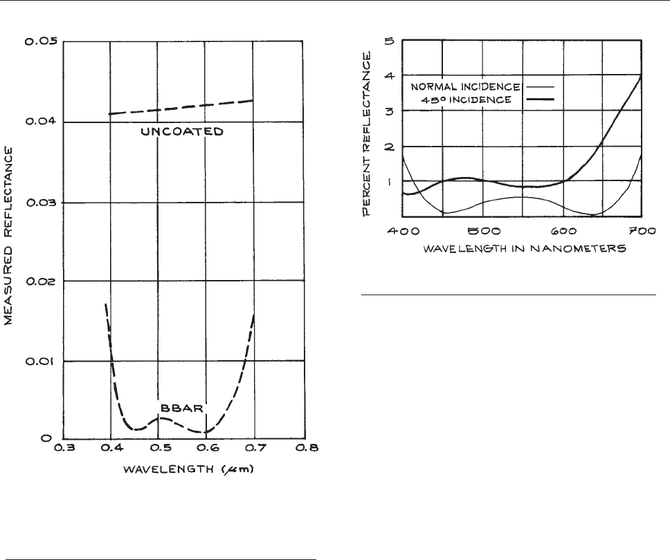
commercially from m any sourc es, as a re coatings of
other types.
31
Some companies offer both optical com-
ponents and coatings, while others specialize in coatings
and will coat customers’ own materials. Melles Griot
offer a HEBBAR (high efficiency broad-band antireflec-
tion) coating that provides very low reflectance over a
broad bandwidth, and is relatively insensitive to angle of
incidence, as shown in Figure 4.33.
(iii) High-reflectance coatings. The usually high reflec-
tance of a metal surface can be further enhanced, as shown
in Figure 4.34(a), by a multiple dielectric coating consist-
ing
of an even number of layers, each a quarter wavelength
thick, and of alternately high and low refractive index, with
a low-refractive-index material next to the metal. A very
high reflectance over a narrow wavelength range can be
achieved, as shown in Figure 4.34(b), by using a dielectric
substrate,
such as fused quartz, and an odd number of
quarter-wavelength layers of alternately high and low
refractive index with a high-index layer on the substrate.
Broad-band high-reflectance coatings are also available
where the thickness of the layers varies around an average
value of a quarter wavelength.
Beamsplitters. Beamsplitters are semitransparent mir-
rors that both reflect and transmit light over a range of wave-
lengths. A good beamsplitter has a multilayer dielectric
coating on a substrate that is slightly wedge-shaped to elim-
inate interference effects, and antireflection-coated on its
back surface to minimize ghost images. The ratio of reflec-
tance to transmittance of a beamsplitter depends on the
polarization state of the light. The performance is usually
specified for light linearly polarized in the plane of inci-
dence (P-polarization) or orthogonal to the plane of inci-
dence (S-polarization). Cube beamsplitters are pairs of
identical right-angle prisms cemented together on their
hypotenuse faces. Before cementing, a metal or dielectric
semireflecting layer is placed on one of the hypotenuse
Figure 4.32 Reflectance of a typical broad-band antireflec-
tion coating (BBAR) showing considerable reduction in
reflectance below the uncoated substrate. (From Handbook
of Lasers, R.J. Pressley (Ed.), CRC Press, Cleveland, 1971; by
permission of CRC Press, Inc.
Figure 4.33 The reflectance spectrum of an HEBBAR
high reflectance broad-band coating.
OPTICAL COMPONENTS 185
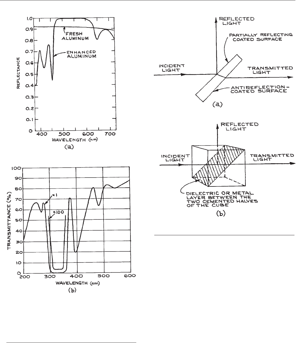
faces. Antireflection-coated cube prisms have virtually no
ghost image problems and are more rigid than plate type
beamsplitters. The operation of both types of beamsplitter is
illustrated in Figure 4.35.
Pellicles. Pellicles are beam-splitting mirrors made of
a high-tensile-strength polymer stretched over a flat
metal frame. The polymer film can be coated to modify
the reflection–transmission characteristics of the film.
The polymer generally used, nitrocellulose, t ransmits in
the visible and near infrared to about 2lm. These devices
have some advantages over conventional coated-glass
or quartz beamsplitters; the thinness of the polymer
Figure 4.34 (a) Reflectance of a plain aluminum mirror
and an aluminum mirror with four dielectric overlayers.
(From Handbook of Lasers, R.J. Pressley (Ed.), CRC Press,
Cleveland, 1971; by permission of CRC Press); (b) typical
transmittance characteristic of a narrow-band,
maximum-reflectance, multilayer dielectric coating on
a dielectric substrate.
Figure 4.35 (a) Conventional planar beamsplitter (wedge
angle greatly exaggerated); (b) cube beamsplitter.
186 OPTICAL SYSTEMS
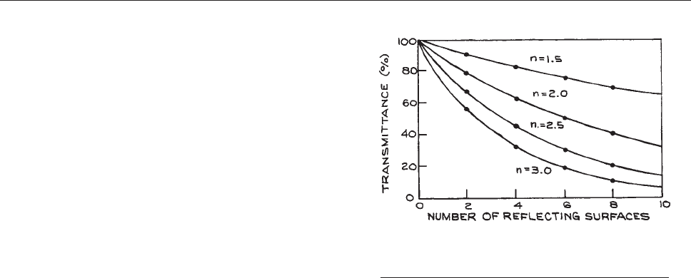
film virtually eliminates spherical and chromatic aberrations
(see Section 4.3.3) when diverging or converging light
pa
sses through them, and ghost-image problems are
virtually eliminated. They will, however, produce some
wavefront distortion, typically about two waves per
inch, and are not suitable for precision applications.
Pellicles are available from several suppliers
31
,suchas
Edmund Optics, Melles Griot, National Photocolor, and
Newport.
4.3.2 Windows
An optical window serves as a barrier between two media,
for example, as an observation window on a vacuum system
or on a liquid or gas cell, or as a Brewster window on a
laser. When light passes through a window that separates
two media, there is, in general, some reflection from the
window and a change in the state of polarization of both the
reflected and the transmitted light. If the window material is
not perfectly transparent at the wavelength of interest, there
is also absorption of light in the window, which at high light
intensities will cause the window to heat. This will cause
optical distortion of the transmitted wave, and at worst – in
high-power laser applications – damage the window on its
surface, internally, or both. Additionally, if the two surfaces
of a window are both very flat (roughly speaking, one wave
per centimeter or better) and close to parallel, the window
will act as an etalon (see Sections 4.3.8 and 4.7.4) and
exhibit distinct variations in transmission with wavelength.
To circumvent this difficulty, which is a particular nuisance
in experiments using lasers, most precision flat optical
windows are constructed as a slight wedge, with an angle
usually about 309.
The details of the reflection, refraction, and change of
polarization state that occur when light strikes a window
surface are dealt with in detail in Sections 4.2.6 and 4.3.6.
These considerations also apply when light strikes a lens or
prism. The reflection at such surfaces can be reduced by a
single-layer or multilayer dielectric antireflection coating. In
optical systems such as multielement camera lenses, where
light crosses many such surfaces, antireflection coatings are
very desirable. Otherwise a severe reduction in transmitted
light intensity will result, as illustrated in Figure 4.36.
Optical
cells, or cuvettes, are transparent containers,
generally made of glass or fused quartz, which are used
in absorption and fluorescence spectrophotometers, in
light-scattering and turbidity measurements, and in many
other specialized experiments. These cells are usually rec-
tangular or cylindrical in shape and are available in many
sizes and configurations, including provision for liquid
circulation. Suppliers include Harrick Scientific, Hellma,
International Crystal Laboratories, Newport/Oriel, NSG
Precision Cells, Optiglas, Spectrocell, and Starna.
4.3.3 Lenses and Lens Systems
Singlet Lenses. Singlet lenses are the simplest and
most readily available lenses for nonexacting applications.
They come in six basic formats, shown in Figure 4.37.The
le
ns is specified by the material of which it is made, the
curvatures R
1
and R
2
of its two faces, the thickness d of
the lens at its mid point, and its aperture diameter D,
which also indirectly specifies its thickness at the edge.
The lens has an effective focal length (EFL), f measured
from its principal planes, and front and back focal lengths,
which specify the distances of the focal points from the front
and back surfaces of the lens, as shown in Figure 4.38.A
bi
convex lens has two generally spherical surfaces. In the
standard sign convention the first of these has a positive
radius and the second a negative radius. A symmetrical
biconvex lens has R
1
¼ – R
2
.Aplano-convex lens has one
flat face, while a convex meniscus lens has a first surface of
positive radius and a second surface of a larger positive
radius. Biconvex, plano-convex, and convex meniscus
Figure 4.36 Transmittance of a multielement optical
system as a function of the refractive index of the
elements.
OPTICAL COMPONENTS 187
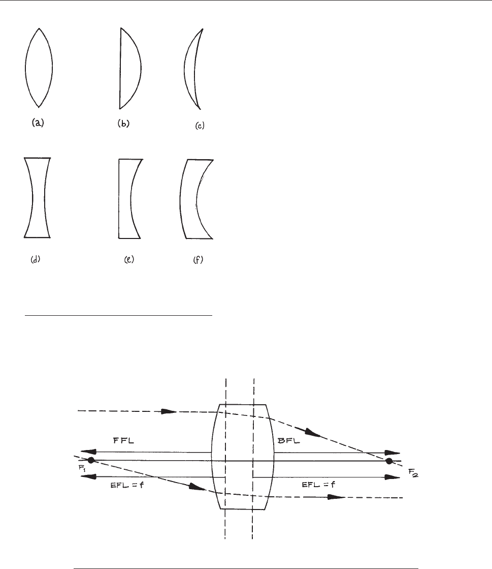
lenses all have a positive EFL. Biconcave, plano-concave,
and concave meniscus lenses have surface curvatures,
opposite in sign to their convex counterparts, and all have
anegativeEFL.
All singlet lenses suffer from spherical and chromatic
aberration. They are inexpensive, but suffer from significant
amounts of aberration, so are not a good choice in imaging
situations. For focusing parallel light (infinite object con-
jugate), or for producing a parallel beam of light, plano-
convex lenses or convex meniscus lenses that are close to
plano-convex exhibit the least spherical aberration for a
specified EFL. For best performance in these applications
the parallel light should pass through the more strongly
curved of the two surfaces. For imaging at different con-
jugate ratios the shape of singlet that produces the least
spherical aberration is called the best form lens for that
application. For example, for equal object and image dis-
tances (conjugate ratio ¼ 1) the best form singlet is a sym-
metrical biconvex lens. Singlet lenses can provide
satisfactory performance provided they are used with rel-
atively large f/numbers. If singlet lenses are used with
lasers then there is no chromatic aberration.
Doublets. If a positive focal length lens of one type of
glass is combined with a weaker negative lens made from a
different type of glass, then the lens combination can
exhibit reduced spherical and chromatic aberration.
Figure 4.37 The six basic singlet lens types:
(a) biconvex; (b) plano-convex; (c) convex
meniscus; (d) biconcave; (e) plano-concave;
(f) concave meniscus.
Figure 4.38 Diagram showing the effective focal length (EFL), the front focal length (FFL),
and the back focal length (BFL) of a thick lens.
188 OPTICAL SYSTEMS
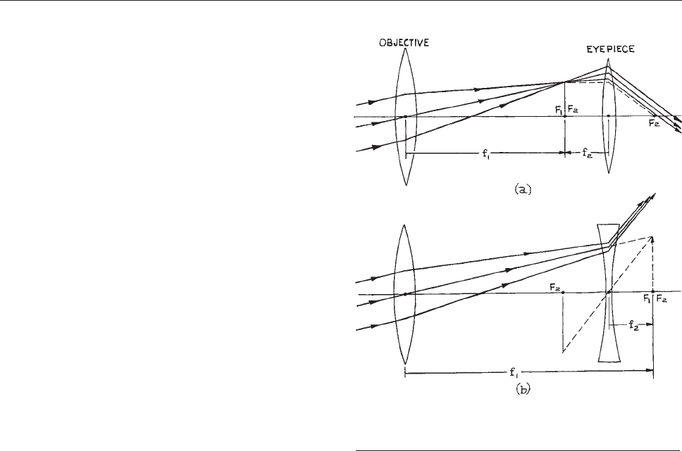
Doublets can be either air-spaced or cemented. They are
widely available from many suppliers, such as CVI/Melles
Griot, Newport Corporation, OptoSigma, Rolyn, and
Thorlabs. For laser applications, even without the
concern for chromatic aberration, doublets will provide
superior focusing performance to singlets.
Camera lenses. Compound lenses involve more than
two spherical surfaces and can be designed to have reduced
aberrations. Camera lenses are multi element compound
lenses especially designed for imaging applications.
A wide variety of high-performance camera lenses is
available commercially from companies such as Canon,
Fujinon, Kodak, Leitz, Minolta, Nikon, Olympus, Sigma,
and Zeiss. The choice of camera lenses for a specific
application is generally guided by two parameters: (i) the
field of view (FOV), which can be specified by the apex
angle of the cone of light that can be collected by the lens
and (ii) the aperture of the lens. Both these parameters
influence the light-gathering power of the lens.
Telecentric lenses are special compound lenses used in
applications such as machine vision and lithography where
object or image movement does not produce a change in
magnification.
33,38
For a lens with object space telecentric-
ity, a change in the object distance will not result in the
image changing size. For such a lens the aperture stop is
located in the back focal plane and the entrance pupil is at
infinity. All the principal rays in object space are parallel to
the axis. For a lens with image space telecentricity, moving
the image plane to focus or defocus the system will not
change the size of the image. In this case the aperture stop
is located in the front focal plane and the exit pupil is at
infinity. In the image space all the principal rays are parallel
to the axis. If a lens is telecentric for both the object
and image spaces it is called doubly telecentric. The primary
disadvantage of telecentric lenses is that they have a very
limited field of view: object and image hav e to lie within a
cylindrical region whose radius in object and image space is
limited by the size of the lens elements. Telecentric lenses
are av ailable from Computer Optics, Edmund Optics,
Mekoptik, Navitar, Opto-Engineering, and Sill Optics.
Simple and Galilean Telescopes. The operation
of a simple telescope is illustrated in Figure 4.39(a).
The
objective is usually an achromat (a lens in which
chromatic aberration – the variation of focal length with
wavelength – has been minimiz ed). I t has a long focal
length f
1
and produces a real image of a distant object,
which can then be examined by the eyepiece lens of focal
length f
2
. This design, which produces an inverted image,
is often called an astronomical telescope. If desired, the
final image c an be erected with a third lens, in which case
the device is called a terrestrial telescope.Theeyepiece
of the telescope can be a singlet lens, but composite eye-
piece designs such as the Ramsden and t he Kellner
11
are
also common. Most large astronomical telescopes use
spherical mirrors as obj ectives, and various configura-
tions are used, such as the Newtonian, C assegrain, and
Schmidt.
11,23–25
Since most telescope development has
been for astronomical applications, it is outside the scope
of thi s book to give a detailed discussion; for further
details the reader should consult Born and Wolf,
11
Levi,
24
Meinel,
38
or Brouwer and Walther.
39
Figure 4.39 Ray paths through telescopes in normal
adjustment (object and final image at infinity):
(a) astronomical telescope; (b) Galilean telescope.
OPTICAL COMPONENTS 189
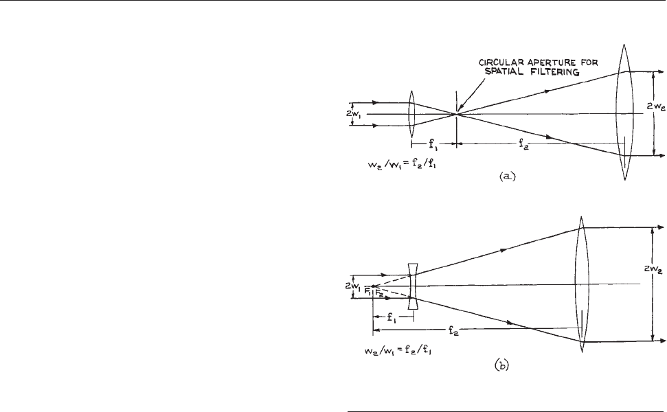
Small astronomical and terrestrial telescopes are widely
available at relatively low cost. Two principal manufac-
turers are Celestron
40
and Meade.
41
The Galilean telescope illustrated in Figure 4.39(b),
first constructed by G alileo in 1609, is the earli est tele-
scope of which there exists definite knowledge. It produ-
ces no real intermediate image, but the final image is
erect. I n normal adjustment, the focal point of the diverg-
ing eyepiece is outside the telescope and coincident with
that of the obje ctive. In th e simple telescope the two focal
points also coincide, but are between the two. The mag-
nification M produced by either type of telescope can be
written as:
M ¼f
1
=f
2
ð4:144Þ
Since the simple telescope has two positive (converging)
lenses, its overall magnification is negative, which indi-
cates that the final image is inverted.
Simple and Galilean telescopes have practical uses in
the laboratory that are distinct from their traditional use for
observing distant objects.
Laser-Beam Expanders and Spatial
Filters.
Laser beams can be expanded and recollimated
(or focused and recollimated) with simple or Galilean tele-
scope arrangements, as illustrated in Figure 4.40. For opti-
mum
recollimation the spacing of the two lenses should be
adjustable, as fine adjustment about the spacing f
2
þ f
1
will
be necessary for recollimating a Gaussian beam. In this
application the Galilean telescope has the advantage that
the laser beam is not brought to an intermediate focus
inside the beam expander. Gas breakdown at such an inter-
nal focus can occur with high-power laser beams, although
this problem can be solved in simple-telescope beam
expanders by evacuating the telescope. Since laser beams
are highly monochromatic, beam expanders need not be
constructed from achromatic lenses. Attempts should,
however, be made to minimize spherical aberration and
beam distortion. It is best to use precision antireflection-
coated lenses if possible. Laser-beam-expanding tele-
scopes that are very well corrected for spherical aberration
are available from Janos, Melles Griot, Newport/Oriel,
Rolyn, Sigma Koki, Space Optics Research Labs, and
Special Optics, among others.
31
Infrared laser-beam
expanders usually have ZnSe or germanium lenses. The
use of biconvex and biconcave lenses distributes the focus-
ing power of the lenses over their surfaces and minimizes
spherical aberration. Better cancellation of spherical aber-
ration is possible in Galilean beam expanders than with
simple telescopes.
If a small circular aperture is placed at the common
intermediate focus of a simple-telescope beam
expander, the device becomes a spatial filter as w ell.
Although ideally the output beam from a laser emitting
aTEM
00
mode has a Gaussian radial intensity profile, in
practice the radial profile may have some irregular struc-
ture. Such beam i rregularities may be produced in the
laser or by passage of the beam through some medium.
If such a beam is focused through a s mall enough aper-
ture and then recollimated, the irregular structure on the
radial intensity profile can be removed and a smooth
Figure 4.40 Laser-beam expanders: (a) focusing type with
spatial filter; (b) Galilean type.
190 OPTICAL SYSTEMS
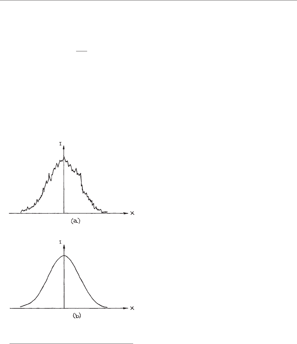
profile restored, as illustrated in Figure 4.41.Thisis
called spatial filtering. The minimum aperture diamete r
that should be used is
D
min
¼
2f
1
k
pw
1
ð4:145Þ
where f
1
is the focal length of the focusing lens and w
1
is
the spot size at that lens. Typical aperture sizes used in
commercial spatial filters for visible lasers are on the order
of 10 lm. This aperture must be accurately and symmetri-
cally positioned at the focal point, so it is usually mounted
on an adjustable XY translation stage.
Lens Aberrations. As discussed in Section 4.2.5, real
lenses suffer from various forms of aberration, which lead
the image of an object to be an imperfect reconstruction of
it. If a particular aberration is judged to be detrimental in a
particular experimental situation, then a special lens combi-
nation can often be obtained that minimizes that aberration –
occasionally at the expense of worsening others.
(i) Chromatic aberrations. Because the refractive index
of the material of a lens varies with wavelength, so does its
focal length. Therefore rays of different wavelengths from
an object form images in different locations. Chromatic
aberration is almost eliminated with the use of an achro-
matic doublet. This is a pair of lenses, usually consisting of
a positive crown-glass lens and a negative flint-glass lens,
cemented together. These two lenses cancel each other’s
chromatic aberrations exactly, at specific wavelengths in
the blue and red, and almost exactly in the region in
between. Good camera lenses are well corrected for chro-
matic aberrations.
Achromatic doublets are available from numerous sup-
pliers, including Edmund Optics.
(ii) Spherical aberration. This aberration can be mini-
mized in a single lens by distributing the curvature
between its two surfaces without altering the focal length.
So, for example, a biconvex lens will produce less spher-
ical aberration than a plano-convex one of the same focal
length. Spherical aberration can be minimized in an ach-
romatic doublet with appropriate choice of curvatures for
the constituent lens elements.
(iii) Coma. When an object point is off the axis of a lens,
its image is produced in different lateral positions by dif-
ferent zones of the lens. Coma can be controlled by an
appropriate choice of lens curvatures.
Other forms of aberration also occur, such as field cur-
vature, in which an object plane orthogonal to the lens axis
is imaged as a curved surface.
(iv) Astigmatism. This aberration can be controlled by
lens curvature and index variations, and by the use of
apertures to restrict the range of angles and off-axis dis-
tances at which rays can traverse the lens.
Aspheric Lenses. If one face of a singlet lens is man-
ufactured as a nonspherical (or aspherical), surface then at
Figure 4.41 Intensity variation I (x) along a diameter
of a TEM
00
laser beam possessing spatial noise
structure: (a) before and (b) after spatial filtering.
OPTICAL COMPONENTS 191
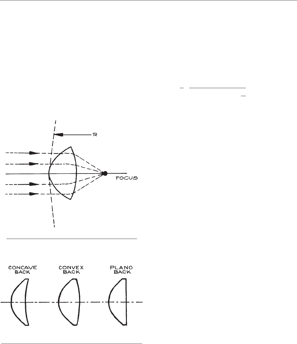
a specified design wavelength all spherical aberration can
be eliminated. With such a lens it is possible to obtain a
much smaller focal length than with a conventional spher-
ical lens of the same diameter, without increasing the
spherical aberration of the lens. An ideal aspheric lens
exactly cancels the spherical aberration that would other-
wise be present in the optical system. Such lenses can
produce the smallest focal spots when used with collimated
laser light. The collimated beam should enter the aspher-
ical surface and the focus will be on the opposite side, as
shown in Figure 4.42. The second face of an aspherical lens
is
often plane, or weakly spherical as shown in Figure 4.43.
If
optimum performance at a particular wavelength and
focal length is required, then a custom asphere can be
manufactured, but this can be expensive, unless a large
number of such lenses are required. Aspheres are often
made by molding, so once the mold has been manufactured
additional lenses are less expensive.
The standard formula that describes an aspheric surface
is:
z ¼
1
R
r
2
1 þ
ffiffiffiffiffiffiffiffiffiffiffiffiffiffiffiffiffiffiffiffiffiffiffiffiffiffiffiffiffiffi
1 ð1 þ KÞ
r
2
R
2
q
þ A
4
r
4
þ A
6
r
6
þA
8
r
8
þ A
10
r
10
þ ð4: 146Þ
where z is the depth (or sag) of the surface, r is the lateral
position, K is the conic constant of the surface, and R is the
effective curvature at the vertex of the surface, as shown in
Figure 4.42. The conic constant K has
the following values
for different surface profiles: K > 0 ellipse, K ¼ 0 sphere,
–1 < K < 0 ellipse, K ¼ –1 parabola, and K < –1 hyperbola.
Most aspherical designs use only the even order terms, as
shown in Equation (4.146), but the odd terms could also be
included.
Aspheric
lenses can collect and focus light rays over a
much larger solid angle than conventional lenses and can
be used at f/numbers as low as 0.6. Aspheric lenses save
space and energy. They can be used as collection lenses
very close to small optical sources, such as high-pressure
mercury or xenon arc lamps, and for collecting radiation
over a large solid angle and focusing it onto a detector
element. Such lenses are often referred to as condensers.
Condensers are widely used in microscopes, where they
focus light from the microscope light source onto a speci-
men. In such applications the aspherical surface should be
on the light source side. Because aspheric lenses are gen-
erally designed only to minimize spherical aberrations,
they will contribute to chromatic aberration, coma, distor-
tion, astigmatism, and curvature of field. Consequently, an
aspheric lens should not be used under circumstances
where these aberrations will be compounded by transmis-
sion through additional components of the optical system.
Glass aspheric lenses are available in a range of diameters
and focal lengths from several suppliers,
31
such as Fresnel
Technologies, Melles Griot, Moritex, OptoSigma, and
Figure 4.42 Focusing light with an aspherical lens.
Figure 4.43 Cross-sections of three common types of
aspheric lens.
192 OPTICAL SYSTEMS

Thorlabs. Aspheric lenses in exotic materials can be
obtained as custom items.
Graded Index Lenses. Small lenses with a
convenient cylindrical shape can be made from graded
index material, which has a refractive index that varies
from point to point inside the material. A commonly
encountered axi-symmetric index variation is Gaussian,
or approximately so. The refractive index as a function
of distance r from the axis of symmetry is:
n ¼ n
0
e
r
2
=2r
2
ð4:147Þ
For distances from the axis that satisfy r r, Equation
(4.147) can be written as
n ¼ n
0
ð1
r
2
2r
2
Þ¼n
0
1
2
n
2
r
2
ð4:148Þ
where n
2
¼ n
0
/r
2
. This is a quadratic index profile. A
cylindrical piece of such transparent material with flat ends
has an overall ray transfer matrix from air, through a length
d of the graded medium and back into air:
AB
CD
¼
10
0 n
0
cos
d
r
r sin
d
r
1
r
sin
d
r
cos
d
r
!
10
01=n
0
¼
cos
d
r
r
n
0
sin
d
nr
n
0
r
sin
d
r
cos
d
r
!
ð4:149Þ
The focal length of this GRIN lens is:
f ¼
r
n
0
sin
d
r
ð4:150Þ
which can also be written as:
f ¼
1
ffiffiffiffiffiffiffiffiffi
n
0
n
2
p
sinðd
ffiffiffiffiffiffiffiffiffiffiffiffi
n
2
=n
0
p
Þ
ð4:151Þ
Rays that enter a graded index lens follow sinusoidal
paths until they reach the back surface of the lens. The
oscillation pattern inside the lens describes its pitch. Figure
4.
44 shows schematically how the pitch is defined. A 1/4
pi
tch graded index lens, for example, will take input parallel
light and bring it to a focus at the exit face of the lens.
Graded index lenses are very convenient to use in small
optical arrangements because their flat ends make them easy
to couple to other structures, such as semiconductor lasers or
optical fibers. They are available commercially as GRIN or
SELFOC lenses from suppliers such as LINOS Photonics,
Melles Griot, NSG, Red Optronics, Schott, and Thorlabs.
These lenses should not be used in precision imaging
applications because they generally suffer from relatively
severe aberrations, especially chromatic aberration.
Fresnel Lenses. A Fresnel lens is an aspheric lens
whose surface is broken up into many concentric annular
rings. Each ring refracts incident rays to a common focus,
so that a very large-aperture, small f/number, thin aspheric
lens results. Figure 4.45 illustrates the construction and
focusing
characteristics of such a lens. These lenses are
generally manufactured from precision-molded acrylic.
Because the refractive index of acrylic varies little with
wavelength, from 1.51 at 410 nm to 1.488 at 700 nm, these
lenses can be very free of chromatic and spherical aberra-
tion throughout the visible spectrum. Fresnel lenses should
Figure 4.44 Schematic operation of graded index lenses:
(a) a quarter pitch lens, which can be used to either focus
parallel light or collimate light from a point source on one
face of the lens; (b) a half pitch lens, which inverts an image
at its front face; (c) a three quarter pitch lens; (d) a whole
pitch lens.
OPTICAL COMPONENTS 193
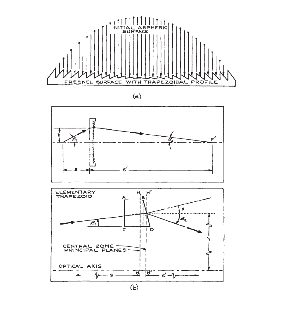
Figure 4.45 (a) A Fresnel lens, made up of trapezoidal concentric secti ons (it
replaces a bulky asp heri c lens); (b) illustration of how the focusing characteristics
of a Fresnel lens result from refraction at the individual surface grooves. (Courtesy
of Melles Gri ot, I nc.)
194 OPTICAL SYSTEMS
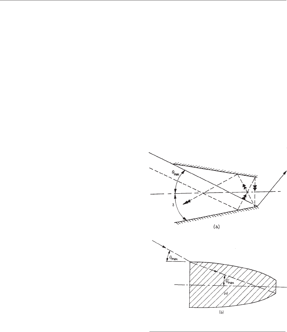
be used so that they focus to the plane side of the lens, and
their surfaces should not be handled. They are inexpensive
and available from very many suppliers, including
Edmund Scientific, Fresnel Technologies, Lexitek, New-
port/Oriel, and Wavelength Optics. They should not be
considered for use in applications where a precision image
or diffraction-limited operation is required. Fresnel lenses
also scatter much more light than conventional lenses.
Fresnel lense s ar e an example of a more general
class of optics called d iffractive optics. These are struc-
tured optical elements that use diffraction to redirect
light, split a light beam into many separate beams, focus
light, produce di ffuse light, or c orrec t di storte d wave-
fronts. They are available from Holographix, MEMS Opti-
cal, Optocraft, RPC Photonics, Silios Technologies, and
Stocker Yale.
Cylindrical Lenses. Cylindrical lenses are pla nar
on one side and cylindrical on the other. I n planes
perpendicular to the cylinder axis they have focusin g
properties identical to a sph erical lens, but they do not
focus at all in planes containing the cylinder axis.
Cylindrical lenses focus an extended source into a
line, and so are very useful for imaging s ources onto
monochromator slits, although perfect matching of
f/numbers is not possible in this way. These lenses are
also widely used for focusing the output of solid-state
and nitrogen lasers into a line image in the dye cell of dye
lasers (see Section 4.6.3). Cylindrical lenses are
a
vailable from Bond Optics, Esco, Infrared Optical
Products, Melles Griot, Newport/Oriel, OFR (now
Thorlabs), Optimax, and Rolyn.
Optical Concentrators. Optical concentrators are
nonimaging light collectors that are useful in delivering
light to a detector. They effectively increase the
collection area of the detector, although they affect the
angles of light rays.
If light enters an optical system of entrance aperture
diameter 2a over a range of angles 2h and leaves through
an aperture of diameter 2a9 over a range of angles 2h9 then
in the paraxial approximation:
ah ¼ a
0
h
0
ð4:152Þ
which follows from the brightness theorem. If the refrac-
tive indices of the input and output media are n, n9, respec-
tively, then this relation becomes:
nah ¼ n
0
a
0
h
0
ð4:153Þ
The quantity n
2
a
2
h
2
, which is unchanged in going through
the system, is called the e
´
tendue of the system. Figure 4.46
shows two simple concentrator designs, a linear conical
concentrator
, and a compound parabolic concentrator
(CPC), often called a ‘‘Winston’’ Cone. These devices
are hollow or solid cones, which reflect entering rays one
or more times before they leave the exit aperture. The
range of light angles leaving such a device is greater than
the range of light angle entering, by the linear ratio be-
tween the entrance and exit apertures. Such a nonimaging
light collector could be used to collect light from a
diffusely emitting source and direct it onto a small area
Figure 4.46 Simple optical concentrator designs: (a) linear
cone; (b) compound parabolic concentrator.
OPTICAL COMPONENTS 195
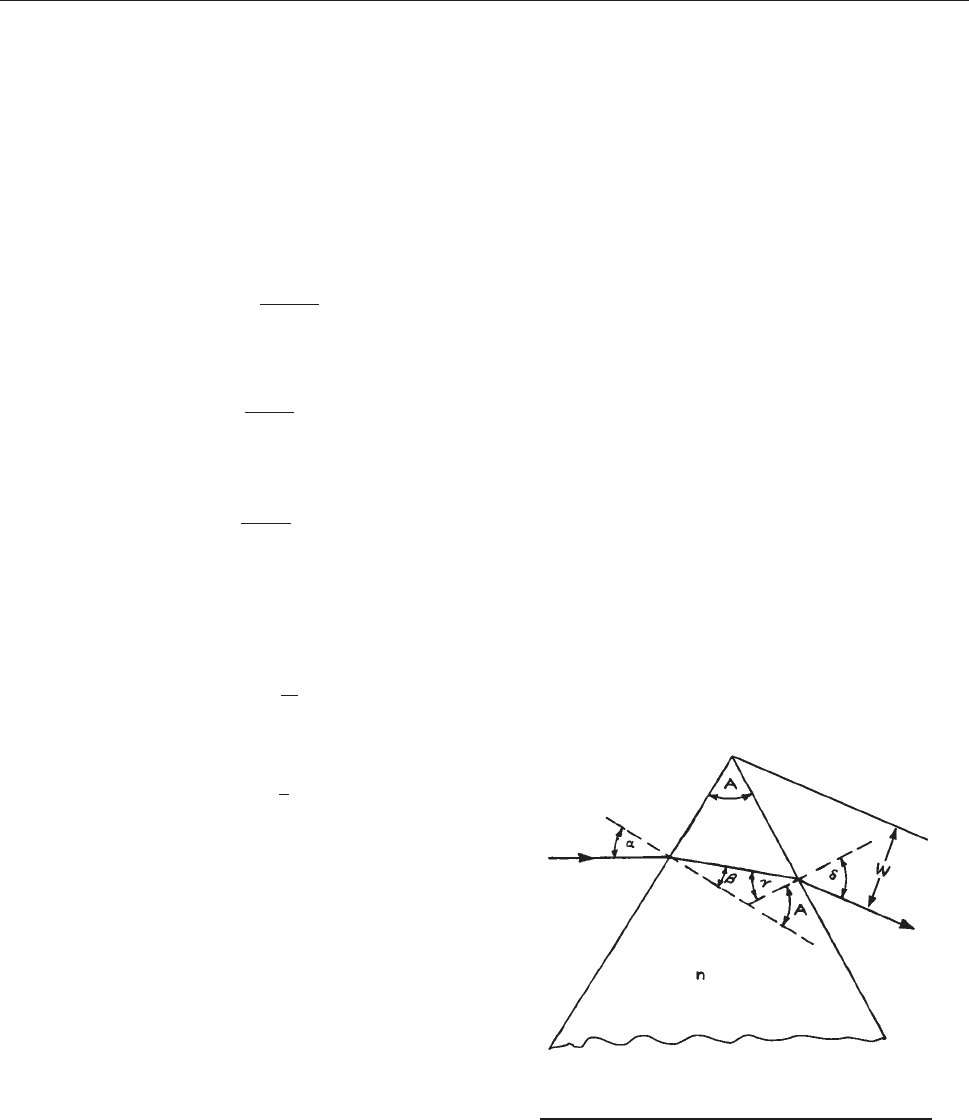
photoelector; however, the detector’s active surface must
be placed close to the exit aperture because of the larger
range of angles of the emerging light rays.
Nonimaging light collectors are useful for collecting
light whose spatial distribution may be fluctuating, yet
whose overall power may remain relatively constant, for
example, in the case of a laser beam that has passed
through a fluctuating medium.
The concentration ratio is:
42,43
C ¼ a=a
0
¼
n
0
sin h
0
n sin h
ð4:154Þ
In 2-D the maximum concentration ratio is:
C
max
¼
n
0
n sin h
ð4:155Þ
and in 3-D for an axisymmetric concentrator:
C
max
¼
n
0
n sin h
2
ð4:156Þ
The CPC can be fabricated from a solid transparent
material with refractive index n. For total internal reflec-
tion to occur for all internal rays that enter within a range
of angles h:
sin h
0
1
2
n
2
ð4:157Þ
or
sin h < n
2
n
ð4:158Þ
To be useful as a material for a CPC it is clear that
n >
ffiffiffi
2
p
.
Since the rays leaving a concentrator can cover a solid
angle up to 2p sr, when the maximum concentration ratio
is used, a detector used in conjunction with the concentra-
tor would need to have its photosensitive surface directly at
the exit aperture.
Simple concentrators can be made by direct machining of
plastic material such as lexan (refractive index ~ 1.585)
using a numerically controlled lathe, followed by polishing.
Alternatively, a stainless-steel mandrel could be machined to
the required shape, and then a mold made by electroplating
over the stainless steel. After the hollow mold is made, then
plastic concentrators can be fabricated using transparent
epoxy resin placed into the mold and allowed to harden.
4.3.4 Prisms
Prisms are used for the dispersion of light into its various
wavelength components and for altering the direction of
beams of light. Prisms are generally available in most
materials that transmit ultraviolet, visible, and infrared
light. High-refractive-index semiconductor materials, such
as silicon, germanium, and gallium arsenide, however, are
rarely used for prisms. Consult Section 4.4 for a list of
suppliers
of optical materials.
The deviation and dispersion of a ray of light passing
through a simple prism can be described with the aid of
Figure 4.47. The various angles a, b, c, d satisfy
Snell’s law
irrespective of the polarization state of the input beam,
provided the prism is made of an isotropic material. It is
easy to show that:
sin d ¼ sin Aðn
2
sin
2
aÞ
1=2
cos A sin a ð4:159Þ
and:
D ¼ a þ d A ð4:160Þ
where A is the apex angle shown in Figure 4.47. The exit
ray
will not take the path shown if c is greater than the
critical angle.
Figure 4.47 Passage of a ray of light through a
prism.
196 OPTICAL SYSTEMS
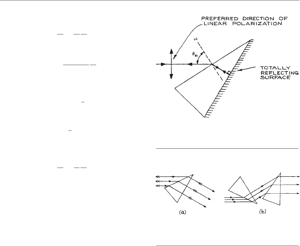
The dispersion of the prism is defined as:
dd
dk
¼
dd
dn
dn
dk
ð4:161Þ
Substituting from Equation (4.159), this becomes:
dd ¼
sin A
cos b cos d
dn
dk
ð4:162Þ
When the prism is used in the position of minimum
deviation:
b ¼ c ¼
1
2
A ð4:163Þ
and:
a ¼ d ¼
1
2
ðD
min
þ AÞð4:164Þ
By the sine rule, Equation (4.162) can be written in the
form:
dd
dk
¼
t
W
dn
dk
ð4:165Þ
where t is the distance traveled by the ray through the
prism and W is the dimension shown in Figure 4.47.
A
simple, yet important, application of a prism as a dis-
persing element is in the separation of a laser beam con-
taining several well-spaced wavelengths into its constituent
parts. Situations where this might be necessary include
isolation of the 488.8 nm line in the output of an argon
ion laser oscillating simultaneously at 476.5, 488.8, and
514.5 nm and other lines, or in nonlinear generation where
a fundamental and second harmonic must be separated. If
the spatial width of the laser beam is known, then an equa-
tion such as (4.165) will determine at what distance from
the prism the different wavelengths are spatially separated
from each other. The advantages of prisms in this applica-
tion are that they can introduce very little scattered light,
produce no troublesome ghost images, and can be cut so
that they operate with a ¼ d ¼ h
B
, thereby eliminating
reflection losses at their surfaces. Brewster-angle prisms
are used in this way inside the cavity of a laser to select
oscillation at a particular frequency. A modified prism
called a reflecting Littrow prism is frequently used in this
way, as shown in Figure 4.48. A Littrow prism is designed
so
that for a particular wavelength the refracted ray on
entering the prism travels normal to the exit face. Thus, if
the exit face is reflectively coated, for the specified wave-
length the incident light is returned along its original path.
Generally, a dispersing optical element used in Littrow has
this retroreflective characteristic at a particular wavelength.
If a beam of parallel monochromatic light passes
through a prism, unless the prism is used in the symmet-
rical minimum-deviation position, the width of the beam
will be increased or decreased in one dimension. This
effect is illustrated in Figure 4.49. By the use of two iden-
tical
prisms in an inverted configuration, the compression
or expansion can be accomplished without an angular
Figure 4.48 Reflecting prism used in Littrow at Brewster’s
angle. Only light of a specific wavelength will be refracted at
the entrance face of the prism and then reflected back on
itself at the coated reflecting face.
Figure 4.49 (a) One-dimensional beam expansion
(or compression) with a prism; (b) one-dimensional beam
expansion without beam deflection using two oppositely
oriented, similar prisms.
OPTICAL COMPONENTS 197
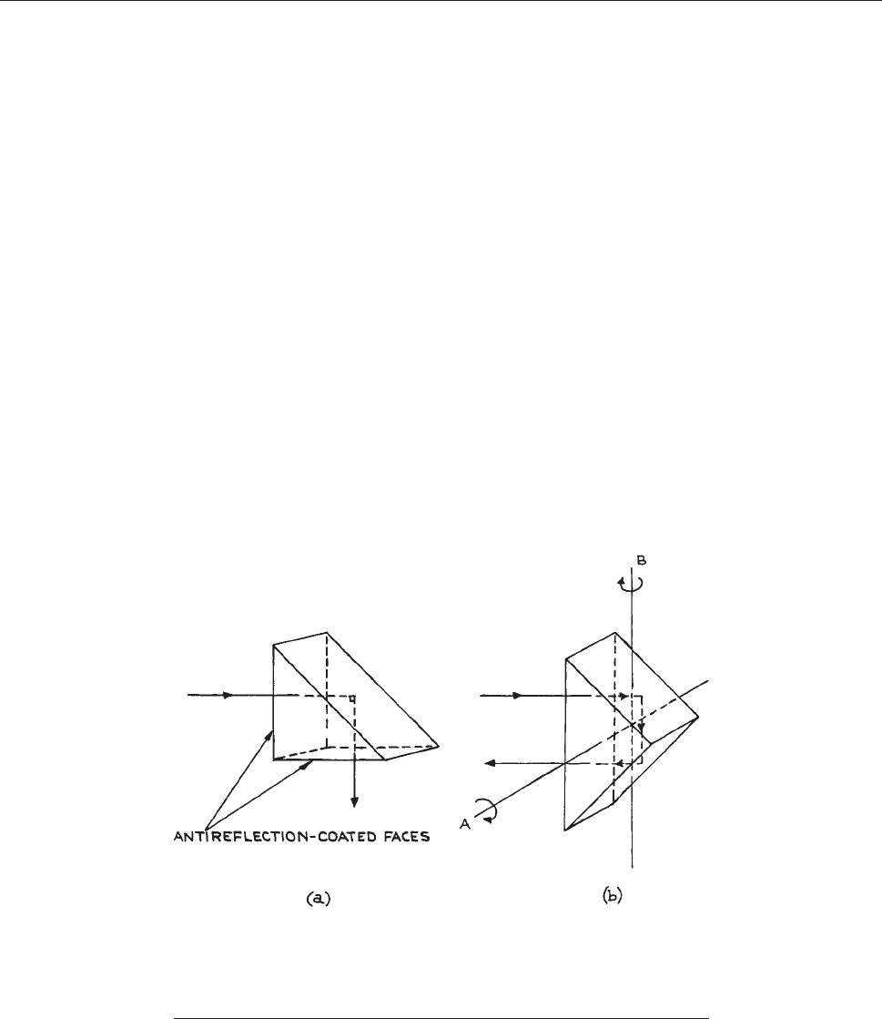
change in beam direction. Prism beam expanders employ-
ing this principle are used in some commercial dye lasers
for expanding a small-diameter, intracavity laser beam
onto a diffraction grating to achieve greater laser line nar-
rowing. Such prism pairs can be used, in conjunction with
lenses, to produce anamorphic laser beam expanders.
These devices are important for the circularization and
collimation of the beams from semiconductor lasers. These
lasers generally emit an elliptical-shaped laser beam whose
beam divergence angle is different in two orthogonal
planes containing the beam axis.
Triangular prisms with a wide range of shapes and ver-
tex angles are available. The most common types are the
equilateral prism, the right-angle prism, and isosceles and
Littrow prisms designed for Brewster-angle operation.
Such prisms are readily available in glass and fused silica
from many suppliers.
31
Triangular and other prisms also
find wide use as reflectors, utilizing total internal reflection
inside the prism or a reflective coating on appropriate
faces. Some specific reflective applications of prisms are
worthy of special note.
Right-Angle Prisms. Right-angle prisms can be used
to deviate a beam of light through 90°, as shown in Figure
4.50(a). Antireflection coatings on the faces shown are
de
sirable in exacting applications. A right-angle prism can
also be used to reflect a beam back parallel to its original
path, as shown in Figure 4.50(b). The retroreflected beam
is
shifted laterally. The prism will operate in this way
provided the incident beam is in the plane of the prism
cross-section. The retroreflection effect is thus independ-
ent of rotation about the axis A in Figure 4.50(b). If the
angle
of incidence differs significantly from zero, the roof
faces of the prism need to be coated; otherwise total inter-
nal reflection at these surfaces may not result. If such a
prism is rotated about the axis B, only in a single orienta-
tion does retroreflection result. Roof prisms are available
from numerous suppliers, including Ealing, Edmund
Scientific, Melles Griot, Newport/Oriel, Opto-Sigma, and
Rolyn.
Porro prisms are roof prisms with rounded corners on
the hypoten use face and beveled edges. They are widely
Figure 4.50 (a) Right-angle prism used for 90° beam deflection;
(b) right-angle prism used for retroreflection. Incident and reflected ray are
parallel only if the incident beam is in the plane of the prism cross-section;
however, in this orientation, retroreflection is independent of orientation
about the axis A within a large angular range.
198 OPTICAL SYSTEMS
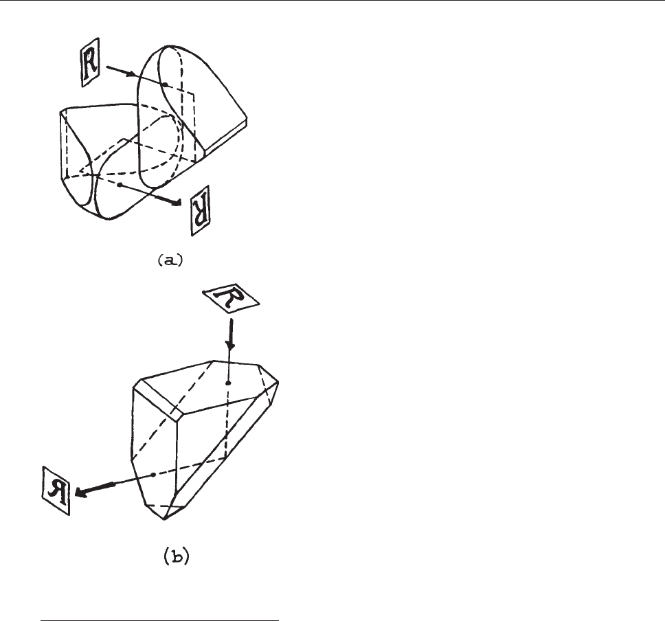
used in pairs for image erection in teles copes and binoc-
ulars, as shown in Figure 4.51(a). They are available from
Anchor
Optics, Edmund Optics, and Sunny Precision
Optics. Ami ci prisms are right-angle prisms where the
hypotenuse face has b een replaced by a 90° roof. They
are available from Anchor Optics, Edmund Optics, Red
Optronics, Starna, and TrustOptics. An image viewed
through an Amici prism is left-to-right reversed
(reverted) and top- to-bottom inve rted, as shown in Figure
4.5
1(b).
Dove, Penta, Polygon, Rhomboid, and Wedge
Prisms.
These prisms are illustrated in Figure 4.52.
Dove prisms are used to rotate the image in optica l
systems; rotation of the prism at a given angular rat e
causes the image to rotate at twice this rate. Dove prisms
have a length- to- aper tur e ratio of about five, so they must
be used with reasonably well-collimated light. They are
available from Anchor Optics, Edmund Opti cs, Esco
Optics, Melles Griot, Newport, Red Optronics, Rolyn,
TrustOptics, and Sunny Precision Optics.
Penta prisms deviate a ray of light by 90° without
inversion (turning upside down) or reversion (right-left
reversal) of the image. This 90° deviation appli es to all
rays incident on the useful aperture of the prism, irre-
spective of the ir angle of incidence. Penta prisms do not
operate by total internal reflection, so their reflective
surfaces are coated. Thes e prisms are useful for 90° devi-
ation when vibrations or other effects prevent their align-
ment being well controlled. They are available from
Anchor Optics, Edmund Optics, Melles Griot, Opto-
Sigma, Red Optronics, Rolyn, Sunny Precision Optics,
and TrustOptics.
Polygon prisms, usually octagonal, are available from
Rolyn and are used for high-speed light-ray deviation, for
example, in high-speed rotary prism cameras.
Rhomboid prisms are used for lateral deviation of a light
ray. When used in imaging applications, there is no change
of orientation of the image. Rhomboid prisms are available
from Edmund Optics, JML Optical, Precision Glass and
Optics, and Rolyn.
Wedge prisms are used in beam steering. The minimum
angular deviation D of a ray passing through a thin wedge
prism of apex angle A is:
D ¼ arcsinðn sin AÞA ’ðn 1ÞA ð4:166Þ
where n is the refractive index of the prism material.
A combination of two identical wedge prisms can be
used to steer a light ray in any direction lying within a cone
of semivertical angle 2D about the original ray direction.
Wedge prisms are available from Anchor Optics, Edmund
Figure 4.51 (a) Two Porro prisms used as an
image-erecting element; (b) Amici prism.
(Courtesy of Melles Griot, Inc.)
OPTICAL COMPONENTS 199
Optics, EKSPLA, Melles Griot, Precision Glass and Optics,
Red Optronics, Rolyn, and Sunny Precision Optics.
Corner-Cube Prisms (Retroreflectors). Corner-
cube prisms are exactly what their name implies, prisms
with the shape of a corner of a cube, cut off orthogonal to
one of its triad (body-diagonal) axes. The front face of the
resultant prism is usually polished into a circle as shown in
Figure 4.53. As a result of three total internal reflections, these
prisms
reflect an incident light ray back parallel to its original
direction, no matter what the angle of incidence is. The
reflected ray is shifted laterally by an amount that depends
on the angle of incidence and the point of entry of the incident
ray on the front surface of the prism. These prisms are
Figure 4.52 (a) Dove prism; (b) penta prism; (c) octagonal prism; (d) rhomboid
prism; (e) wedge prism, [(a), (b), and (e) courtesy of Melles Griot, Inc.]
200 OPTICAL SYSTEMS
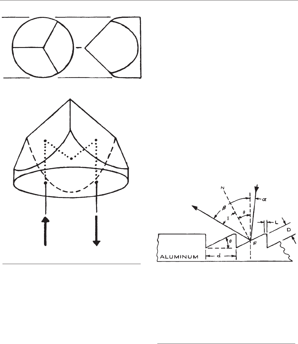
in v aluable in experiments where a light beam must be
reflected back to its point of origin from some (usually
distant) point – for example, in long-path absorption
measurements through the atmosphere with a laser beam.
They are available commercially from Edmund Optics,
Knight Optical, Melles Griot, Newport, Precision Glass
and Optics, Precision Optical, Red Optronics, Rolyn, and
Sunny Precision Optics. The angular deviation of the
reflected ray from its original direction can be held to less
than a half second of arc in the best prisms. For infrared
applications beyond the transmission of fused silica, corner-
cube prisms are not readily available, but retroreflectors
can be made by using three square mirrors butted
together to form a hollow cube corner. Precision hollow
corner cubes of this type are available from PLX.
4.3.5 Diffraction Gratings
A diffraction grating is a planar or curved optical surface
covered with straight, parallel, equally spaced grooves.
They are manufactured in three principal ways: by direct
ruling on a substrate (called a master grating), by replication
from a master grating, and holographically. Such gratings
can be made for use in transmission, but are more com-
monly used in reflection. Light incident on the grooved face
of a reflection grating is diffracted by the grooves; the angu-
lar intensity distribution of the diffracted light depends on
the wavelength and angle of incidence of the incident light
and on the spacing of the grooves. This can be illustrated
with reference to the plane grating shown in Figure 4.54.
Th
e grooves are usually produced in an aluminum or gold
Figure 4.53 Corner-cube prism.
(Courtesy of Melles Griot, Inc.)
Figure 4.54 Blazed groove profile. The thickness of the
aluminum is generally equal to the blaze wavelength, and
the depth of the groove is about half the thickness. The
dimensions shown are approximately those for a grating
ruled with 1200 grooves per millimeter, blazed at 750 nm.
D ¼ depth of ruling; d ¼ groove spacing; L ¼ unruled land;
a ¼ angle of incidence; b ¼ angle of diffraction; c ¼ angle
of reflection; h ¼ blaze angle. The line N is normal to the
groove face F. (From D. Richardson, ‘‘Diffraction Gratings,’’
in Applied Optics and Optical Engineering, Vol. 5, R.
Kingslake (Ed.), Academic Press, New York, 1969; by
permission of Academic Press).
OPTICAL COMPONENTS 201

layer that has been evaporated onto a flat optical substrate.
For high-intensity laser applications the substrate should
have high thermal conductivity. Master gratings ruled on
metal are available for this purpose from Diffraction Prod-
ucts, Jobin-Yvon, and Richardson Grating Laboratory
(through Newport). If the light diffracted at angle b from a
given groove differs in phase from light diffracted from the
adjacent groove by an integral multiple m of 2p, a max-
imum in diffracted intensity will be observed. This con-
dition can be expressed as:
mk ¼ dðsin a 6 sin bÞð4:167Þ
The plus s ign applies if the incident and the diffracted
ray lie on the same s ide of the normal to the grating
surface; m is called the order of the diffraction. For m
¼ 0, a ¼ b and the grating acts l ike a mirror. In any other
order, the diffraction maxima of different wavelengths
lie at different angles. The actual distribution of dif-
fracted intensity among the various or ders depe nds on
the profile of the grating grooves. If the grooves are pla-
nar, cut a t an angle h to the plane of the grating, max-
imum diffracted intensity into a particular order results if
the angle of diffraction and the angle of reflection are the
same. In this case:
b h ¼ c ð4:168Þ
h is called the blaze angle. The wavelength for which the
angle of reflection from the groove face and the diffraction
angle are the same is called the blaze wavelength, k
B
.Itis
common to use a grating in a Littrow configuration so that
the diffracted ray lies in the same direction as the incident
ray. In this case:
mk ¼ 2d sin b ð4:169Þ
The wavelength at which the light reflects normally
from the grating groove satisfies:
mk
B
¼ 2d sin h ð4:170Þ
Thus, for example, a grating could be specified to be
blazed at 600 nm in the first order; it would, of course,
be simultaneously blazed in the second order for 300 nm,
the third order for 200 nm, and so on. Gratings are also
available with rectangular shaped (laminar profile) or sinus-
oidal groove profiles. Laminar profile grooves have low
second-order efficiency, which can be advantageous in vac-
uum ultraviolet applications: second-order rejection filters
are not available at such short wavelengths. Sinusoidal gra-
tings will operate over a broad spectral range, but their
diffraction efficiency into a particular order is at best
33%. There are many suppliers of both plane and concave
gratings, particularly Diffraction Products, Digital Optics,
Gentec, Jobin-Yvon, Newport, Optometrics, Spectrogon,
Spectrum Scientific, and TVC Jarrell-Ash.
Resolving Power. The resolving power of a grating is
a measure of its ability to separate two closely spaced
wavelengths. The resolving power depends both on the
dispersion and the size of the grating. For a fixed angle
of incidence, the dispersion is defined as:
db
dk
a
¼
m
d cos b
ð4:171Þ
Thus, the dispersion can be increased by increasing the
number of lines per millimeter (1/d), by operating in a high
order, and by using a large angle of incidence (grazing
incidence). The incidence, however, must not be so flat as
to make the projection of the groove width perpendicular to
the incoming light smaller than the wavelength of the light.
The resolving power of a grating is Dk/k,wherek and k +
Dk are two closely spaced wavelengths that are just resolved
by the grating. The limiting resolution depends on the pro-
jected width of the grating perpendicular to the diffracted
beam. This width is Nd cos b,whereN is the total number
of lines in the grating. Diffraction theory predicts that
the angular resolution of an aperture of this size is
D/ ’ k=ðNd cos bÞ. The angle between the two closely
spaced wavelengths, from the dispersion relation, is:
Db ¼
mDk
d cos b
ð4:172Þ
In the limit of resolution, D/ ¼ Db, which gives:
k=Dk ¼ mN ð4:173Þ
Thus, from Equation (4.167):
k
Dk
¼
Ndðsin a 6 sin bÞ
k
ð4:174Þ
202 OPTICAL SYSTEMS

and so it is clear that large gratings used at high angles give
the highest resolving power. The resolving powers avail-
able from 1 cm wide gratings range up to about 5 3 10
5
.
Concave gratings. These have long been used in short
wavelen gth applications because they provide diffracti v e and
focusing functions simultaneously. The development of
holographic concave gratings has made these devices widely
av ailable. They can be used to correct for aberrations which
occur when they are used in spectrometers (see Section 4.7),
and
to allow compact versions of such instruments to be
produced.
Efficiency. The efficiency of a grating is a measure of its
ability to diffract a given wavelength into a particular order
of the diffraction pattern. Blazing of the grating is the main
means for obtaining efficiency in a particular order;
without it, the diffracted energy is distributed over many
orders. Gratings are available with efficiencies of 95% or
more at their blaze wavelength, so they are virtually as
efficient as a mirror, yet retain wavelength selectivity.
Defects in Diffraction Gratings. In principle, if an
ideal grating is illuminated with a plane monochromatic
beam of light, diffracted maxima occur only at angles that
satisfy the diffraction equation (4.167). In practice,
ho
wever, this is not so. Gratings manufactured by ruling
a metal-coated substrate with a ruling engine exhibit
undesirable additional maxima.
Periodic errors in the spacing of the ruled grooves produce
Rowland ghosts. These are spurious intensity maxima, usu-
ally symmetrically placed with respect to an expected max-
imum and usually lying close to it. The strongest Rowland
ghosts from a modern ruled grating will be less than 0.1% of
the expected diffraction peaks. L yman ghosts occur at large
angular separations from their parent maximum, usually at
positions corresponding to a simple fraction of the wave-
length of the parent maximum – 4=9or5=9, for example.
They are also associated with slo w periodic errors in the
ruling process. Lyman-ghost intensities from modern gratings
are exceedingly weak (0.001% of the parent or less). Ghosts
can be a problem when used for the detection of weak emis-
sions in the presence of a strong laser signal, the ghosts of
which can (and have been) mistakenly identified as other real
spectral lines. If there is any suspicion of this, the weak signal
should be checked for its degree of correlation with the laser
signal – a linear correlation would be strong evidence for a
ghost. The development of unruled holographic gratings,
which are essentially perfect, plus the improvement of ruled
gratings made by interferometrically controlled ruling
engines, has considerably reduced the problem of ghosts.
There are other diffraction-grating defects. Satellites
are misplaced spectral lines, which can be numerous,
occurring very close to the parent, usually so close that
they can only be discerned under conditions of high res-
olution: they arise from small loc al varia tions in groove
spacing. Scattering gives rise to an appare nt weak contin-
uum over all diffraction angles w hen a grating is illumi-
nate d with an intense monochromatic source s uch as a
laser. Sc attering can arise from microscopic dust particles
or nongroove-like, ran dom d efects on the diffraction-
grating surface. In practice it does not follow th at a dif-
fraction grating that sh ows apparent bl emishes, such as
broad, shaded bands, will perform defec tively. One should
never attempt to remove such apparent visual bl emishes
by cleaning or polishing the grating.
Specialized Diffraction Gratings. Concave gra-
tings are frequently used in vacuum-ultraviolet spectrom-
eters and spectrographs, as they combine the functions of
both dispersing element and focusing optics. Thus, fewer
reflective surfaces are required – a highly desirable feature
of an instrument used at short wavelengths, where reflec-
tances of all materials decrease markedly.
Gratings for use at long wavelengths, above 50 lm,
use relatively few grooves per millimeter. Such gratings
are generally ruled directly on metal and are frequently
called echelettes (lit tle ladders) because of the shape of
their grooves.
Echelle gratings are special gratings designed to give
very high dispe rsion, up to 10
6
for ultraviolet wave-
lengths, when operated in a very high order. They have
the surface profile illustrated in Figure 4.55,wherethe
dim
ension D is much larger than in a conventional gra-
ting, and can range up to several micrometers. Echelles
are widely used as the wavelength-tuning elemen t in
pulsed dye lasers because of their high dispersion and
efficient operation. Other uses of diffraction gratings,
such as in the production of M oire
´
fringes and in inter-
ferometers, will not be discussed here. These subjects
have been dealt with by Girard and Jacquinot.
44
OPTICAL COMPONENTS 203
Practical Considerations in Using Diffraction
Gratings.
The main considerations in specifying a dif-
fraction grating are the wavelength region where maxi-
mum efficiency is required (which will specify the blaze
angle), and the number of grooves per millimeter and the
size of the grating (which will determine the resolving
power). Most gratings are rectangular or circular, the latter
being primarily for laser-cavity wavelength selection. Dif-
fraction gratings should be mounted with the care due all
precision components. Their surfaces should never be
touched and should be protected from dust. It is important
to note that if a grating is illuminated with a giv en wave-
length, say 300 nm, then dif fraction maxima will occur in the
same positions as would be found for 600 and 900 nm. This
dif ficulty can be av oided by using appropriate filters to pre-
vent unwanted wavelengths from passing through the system.
4.3.6 Polarizers
Polarized Light. If the electric vector of an
electromagnetic wave always points in the same
direction as the wave propagates through a medium, then
the wave is said to be linearly polarized. The direction of
linear polarization is defined as the direction of the electric
displacement vector D, where:
D ¼ e
r
e
0
E ð4:175Þ
Except in anisotropic media, where e
r
is a tensor, D and
E are parallel and the direction of linear polarization can
be taken as the direction of E. If a combination of
two linearly polarized plane waves of the same frequency,
but having different phases, magnitudes, and polarization
directions, is propagating in the z-direction, the
resultant light is said t o be elliptical ly polarized.Such
a p air of waves, in genera l, have resultant electric fields
in the x-and y -directions t hat can be written as:
E
x
¼ E
1
cos xt ð4:176Þ
E
y
¼ E
2
cosðxt þ /Þð4:177Þ
where / is the phase difference between these two resul-
tant field components. These are the parametric equations
of an ellipse. If / ¼ 6p/2 and E
1
¼ E
2
¼ E
0
, then:
E
2
x
þ E
2
y
¼ E
2
0
ð4:178Þ
which is the equation of a circle. This represents circularly
polarized light. Then the instantaneous angle that the total
electric field vector makes with the x-axis, as illustrated in
Figure 4.56, is:
a ¼ arctan
E
y
E
x
¼ arctan7 tan xt ¼ 7xt ð4:179Þ
Figure 4.56 Instantaneous direction of the electric vector
of an electromagnetic wave.
Figure 4.55 Echelle grating used in Littrow.
204 OPTICAL SYSTEMS
For / ¼ p/2, the resultant electric vector rotates coun-
terclockwiseviewedinthedirectionofpropagation–this
is right-hand circularly polarized light.If/ ¼ –p/2 the
rotation is clockwise – this is left-hand circularly polar-
ized light . The motion of the t otal electric vector as it
propagates is illustrated in Figure 4.57 .If/ ¼ 0o
rp
we have linearly polarized light. Just as circularly p olar-
ized light can be viewed as a superposition of two linearly
polarized waves with orthogonal polarizations, a linearly
polarized wave can be regarded as a superposition of
left- and right-hand circularly po larized waves. If an el ec-
tromagnetic wave consists of a superposition of many
independent linearly p ola rized waves of independe nt
phase, amplitude, and polarization direction, it is said to
be unpolarized.
In anisotropic media – media with lower than cubic
symmetry – there is at least one direction, and at most
two directions, along which light can propagate with no
change in its state of polarization, independent of its state
of polarization. This direction is called the optic axis. Uni-
axial crystals have one such axis; biaxial crystals have
two. When a wave does not propagate along the optic axis
in such crystals, it is split into two polarized components
with orthogonal linear polarizations. In uniaxial crystals
these two components are called the ordinary and extraor-
dinary waves. They travel with different phase velocities,
characterized by two different refractive indices, n
o
and
n
e
(h), respectively, where h is the angle between the k vec-
tor of the wave and the optic axis. This phenomenon is
referred to as birefringence.
D and E are not necessarily parallel in an anisotropic
medium; however, D and H are orthogonal to the wave
vector of any propagating wave. Consequently the Poynt-
ing vector of the wave does not, in general, lie in the same
direction as the wave vector. The direction of the Poynting
vector is the direction of energy flow – the ray direction.
When a plane wave crosses the boundary between an iso-
tropic and an anisotropic medium, the path of the ray will
not, in general, satisfy Snell’s law. The angles of refraction
of the ordinary and extraordinary rays will be different.
This phenomenon is called double refraction. In uniaxial
crystals, however, the ordinary ray direction at a boundary
does satisfy Snell’s law. For further details of these and
other optical characteristics of anisotropic media, the
reader should consult Born and Wolf,
11
Wahlstrom,
12
and Davis.
15
If linearly polarized light propagates into a birefringent
material, unless its polarization direction matches the
allowed direction of the ordinary or extraordinary wave,
it will be split into two components polarized in these two
allowed directions. These two components propagate at
different velocities and experience different phase changes
on passing through the crystal. For light of free-space
wavelength k
0
passing through a uniaxial crystal of length
L, the birefringent phase shift is:
D/ ¼
2pL
k
0
n
e
ðhÞn
o
½ð4:180Þ
In uniaxial crystals the allowed polarization directions
are perpendicular to the optic axis (for the ordinary wave)
and in the plane containing the propagation direction and
the optic axis (for the extraordinary wave), as shown in
Figure 4.57 Left-hand circularly polarized light. (From E.
Wahlstrom, Optical Crystallography, 3rd edn., John Wiley &
Sons, Inc., New York, 1960; by permission of John Wiley &
Sons, Inc.)
OPTICAL COMPONENTS 205
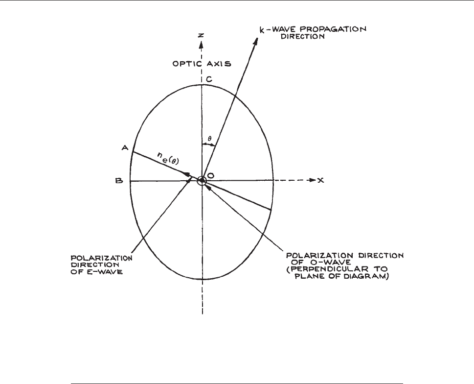
Figure 4.58. If the input wave is polarized at an angle b to
the ordinary polarization direction and D/ ¼ (2n þ 1)p,
the output wave will remain linearly polarized, but its
direction of polarization will have been rotated by an angle
of 2b. This rotation is always toward the ordinary polar-
ization direction, so a round-trip pass through the material
does not affect the polarization state. It is usual to make
b ¼ 45°, in which case the crystal rotates the plane of
polarization by 90°. Such a device is called a (2n þ 1)th-
order half-wave plate. On the other hand, if b ¼ 45° and
D/ ¼ (2n þ 1)p/2, the ordinary and extraordinary waves
recombine to form circularly polarized light. Such a device
is called a (2n + 1)th-order quarter-wave plate.Ifb is not
45°, a quarter-wave plate will convert linearly polarized
light into elliptically polarized light.
Polarization Changes on Reflection. As shown
in Section 4.2.6, if a linearly polarized wave reflects from
a
dielectric surface (or mirror), its state of linear polariza-
tion may be changed. For example, if a vertically polarized
wave traveling horizontally striking a mirror at 45° is
polarized in the plane of incidence, then after reflection
it will be traveling vertically and will be horizontally
polarized. A reflection off a second mirror at 45°,so
Figure 4.58 Cross-section of an ellipsoidal figure called the indicatrix, which allows
determination of the refractive indices and permitted polarization directions of a wave
traveling in a uniaxial crystal. The equation of the ellipse shown is (x
2
/n
0
2
)+(z
2
/n
e
2
) ¼ 1,
where OB ¼ n
o
and OC ¼ n
e
, OA ¼ n(h) is the effective extraordinary refractive index for a
wave traveling at angle h to the optic axis. The ordinary refractive index for this wave is still
n
o
and is independent of h.
206 OPTICAL SYSTEMS
oriented that the plane of incidence is perpendicular to the
polarization, will produce a horizontally traveling, hori-
zontally polarized wave. This exemplifies how successive
reflections can be used to rotate the plane of polarization of
a linearly polarized wave, and is illustrated in Figure 4.59.
If
circular or elliptically polarized light reflects from a
dielectric surface or mirror, its polarization state will, in
general, be changed. As an example, consider reflection at
a metal mirror. From Equations (4.87) and (4.89), for the
in-plane
and perpendicular polarized components of the
incident wave, respectively, we have:
q
jj
¼1
q
?
¼1
ð4:181Þ
These reflection coefficients ensure that the tangential
component of the electric field goes to zero at the conduct-
ing surface of the mirror. As illustrated in Figure 4.60(a)
and
(b), this leads to a conversion of left- to right-hand
circularly
polarized light on reflection. The change of
polarization state on reflection from a dielectric interface
depends on the angle of incidence and whether n
2
> n
1
.
Figure 4.60 Changes of polarization state on reflection:
(a) and (b) conversion of left-hand
circularly polarized light (LHCP) to right-hand
circularly polarized light (RHCP) on reflection at
a perfect metal mirror; (c) conversion of LHCP to linear
polariation on reflection at Brewster’s angle.
Figure 4.59 Rotation of the plane of polarization
of a linearly polarized beam by successive reflection at two
mirrors.
OPTICAL COMPONENTS 207

A special case, illustrated in Figure 4.60(c), shows left-
hand circularly polarized light being converted to linearly
polarized light on reflection from an interface placed at
Brewster’s angle. Such changes of polarization state must
be taken into account when designing an optical system to
work with polarized light. The change in polarization of a
beam of light as it passes through a series of optical com-
ponents can be calculated very conveniently by the use of
Jones or Mueller calculus, which use matrix methods to
describe the state of polarization of the beam and its inter-
action with each component. Details of these techniques
are given by Shurcliff.
13
Linear Polarizers. A linear polarizer changes
unpolarized light to linearly polarized light or changes
polarized light to a desired linear polarization.
The simplest linear polarizers are made from dichroic
materials – materials that transmit one polarizat ion,
either ordinary or extraordinary, and strongly absorb
the other. Modern dichroic l inear polarizers , the com-
monest of which is Pola roid, ar e made of pol ymer films
in which long- chain molecules with appropriate absorb-
ing side groups are oriented by stretching. The stretched
film is then sandwiched between glass or plastic sheets .
These polarizers are inexpensive, but cannot be used to
transmit high intensities because they absorb all polariza-
tions to some degree. They cannot be fabricated to very high
optical quality, and generally only transmit about 50% of
light already linearly polarized for maximum transmission.
They do, however, work when the incident light strikes them
at any angle up to grazing incidence. The extinction coef-
ficient K that can be achieved with crossed polarizers is
defined as:
K ¼ log
10
T
0
T
90
ð4:182Þ
where T
0
and T
90
are the transmittances of parallel and
crossed polarizers, respectively. K is a useful quantity for
specifying a linear polarizer – the larger its value, the
better the polarizer. For dichroic polarizers, values of K
up to about 4 can be obtained. Polarizing beamsplitting
cubes provide linearly polarized light of relatively high
purity (98% or better) and can handle higher light inten-
sities. Corning manufacture a sheet polarizer called
Polacor made from glass containing billions of tiny silver
crystals. This material provides high throughput in the red
to near-infrared region, and extinction up to 4.
Higher quality, but more expensive, linear polarizers can
be made by using the phenomenon of double refraction in
transparent birefringent materials such as calcite, crystal-
line quartz, or magnesium fluoride. Figure 4.61 shows
schematically
the way in which various polarizing prisms
of this type operate. Some of these polarizers generate two
orthogonally polarized output beams separated by an
angle, while others, for example the Glan–Taylor, reject
one polarization state by total internal reflection at a boun-
dary. Extinction coefficients as high as 6 and good optical
quality can be obtained from such polarizers. The accept-
ance angle of these polarizers is generally quite small,
although it can range up to about 38° with an Ahrens
polarizer. Suppliers of polarizing prisms include Argyle
International, Gooch and Housego, Karl Lambrecht Cor-
poration, II-VI Infrared, Inrad, Lambda Research Optics,
Meadowlark Optics, Melles Griot, Newport/Oriel, Opto-
Sigmna, and Precision Optical.
Infrared polarizers (beyond about 7 lm) are often made
in the form of very many fine, parallel, closely spaced
metal wires. Waves with their electric vector perpendicular
to the wires are transmitted; the parallel polarization is
reflected. Such polarizers are available from Coherent/
Molectron, Specac, and Thorlabs.
Linear polarizers for any wavelength where a transpar-
ent window material is available can be made using a stack
of plates placed at Brewster’s angle. Unpolarized light
passing through one such plate becomes slightly polarized,
since the component of incident light polarized in the plane
of incidence is completely transmitted, whereas only about
90% of the energy associated with the orthogonal polar-
ization is transmitted. A pile of 25 plates gives a high
degree of polarization. Stacked-plate polarizers are rather
cumbersome, but they are most useful for polarizing high-
energy laser beams where prism polarizers would suffer
optical damage. They are available commercially from
Inrad and II-VI Infrared (using ZnSe). For visible and
near-infrared light they can be easily made using a stack
of microscope slides.
Retardation Plates. Quarter-wave plates are gener-
ally used for converting linear to circularly polarized light.
208 OPTICAL SYSTEMS
Figure 4.61 Construction of various polarizers using birefringent crystals: (a) Ahrens polarizer – three calcite prisms cemented
together with Canada balsam, whose refractive index is intermediate between n
o
and n
e
for calcite. The O-ray suffers total
internal reflection at the cement and is absorbed in the black coating on the sides; (b) Glan–Foucault polarizer – two calcite
prisms separated with an air gap. The O-ray is totally internally reflected and either absorbed in the sides or transmitted
OPTICAL COMPONENTS 209
They should be used with the optic-axis direction at 45°
to the incident linear polarization direction. They are
available commercially in two forms: multiple- and single-
order. Multiple-order plates produce a phase change (retar-
dation) between the ordinary and extraordinary waves of
(2n +1)p/2. This phase difference is very temperature-
sensitive – a thickness change of one wavelength will pro-
duce a substantial change in retardation. Single-order
plates are very thin, their thickness being:
L ¼
k
0
4ðn
e
n
o
Þ
ð4:183Þ
For example, with calcite, which has n
o
¼ 1.658, n
e
¼
1.486, and with k
0
¼ 500 nm this thickness is only 726.7
nm. Consequently, most single-order plates are made by
stacking a (2n + 1)th-order quarter-wave plate on top of a
2nth-order plate whose optic axis is orthogonal to that of
the first plate. The net retardation is just p/2 and is very
much less temperature-sensitive.
Direct single-order quarter-wave plates for low-inten-
sity applications can be made from mica, which cleaves
naturally in thin slices. The production of a plate for a
particular wavelength is a trial-and-error procedure.
12,45
Quarter-wave plates are invaluable, in combination with
a linear polarizer, for reducing reflected glare and for
reducing back reflections into an optical system, as shown
in Figure 4.62.
Half-wave
plates are generally used for rotating the
plane of polarization of linearly polarized radiation.
Figure 4.62 An optical isolator constructed from a linear polarizer and a
quarter-wave plate.
Caption for Figure 4.61 (cont.) if the sides are polished. A Glan–Thompson polarizer is similar; (c) Glan–Taylor polarizer –
similar to a Glan–Foucault polarizer except for the optic-axis orientation, which ensures that the transmitted E-ray passes
through the air gap nearly at Brewster’s angle; consequently, transmission losses are much reduced from those of a Glan–
Foucault. For high-power laser applications, the side faces can be polished at Brewster’s angle; (d) Rochon polarizer – two calcite
prisms with orthogonal optic axes cemented together with Canada balsam. / depends on the interface angle. The intensities of
the transmitted O- and E-rays are different. Other birefringent materials can be used; in the case of quartz, for example, the E-ray
would exit below the O-ray in the diagram shown here; (e) Senarmont polarizer – two calcite prisms cemented together with
Canada balsam. The angle / depends on h. This type of polarizer is less commonly used than the Rochon polarizer; (f) Wollaston
polarizer – two calcite prisms cemented together with Canada balsam. The O- and E-ray transmitted intensities are different. The
beam separation angle / depends on the interface angle h.
210 OPTICAL SYSTEMS
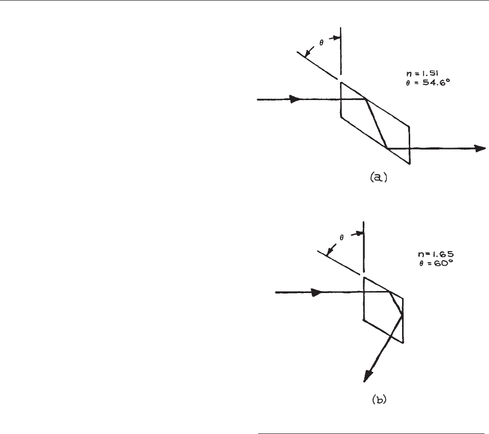
Multiple- and zero-order plates are available; as
in the case of quarter-wave plates, the operating
wavelength must be specified in buying one. This operat-
ing wavelength can be tuned to some extent by tilting
the retardation plate. Half-wave plates cannot be used
to make an optical isolator, as the polarization change
that occurs on one pass through the plate is reversed on
the return path.
Retardation plates only produce their specified retarda-
tion at a particular wavelength, and are usually specified
for normal, or almost normal incidence. Retardation plates
are available from several suppliers, including Karl Lam-
brecht Corporation, Optics for Research, Inrad, II-VI
Infrared, Esco, Melles Griot, Newport, OptoSigma and
Thorlabs. Continuously adjustable retardation plates,
called Babinet-Soleil compensators, are available from
Karl Lambrecht Corporation, Melles Griot, II-VI Infrared,
New Focus, Continental Optical, and OFR (now Thorlabs),
among others.
31
Retardation Rhombs. Because, in general, there is
a different phase shift on total internal reflection for
waves polarized in and perpendicular to the plane
of incidence, a r etarder that is virtually achromatic can
be made by the use of two internal reflections in a
rhomboidal prism of appropriate apex angle and refrac-
tive index. Two examples are shown in Figure 4.63.The
Fresne
l rhomb , for example, use s glass of index 1.51,
and with an apex angle of approximately 54.6° pr oduces
a retardation of exactly 90°. The op timum angle
must, h owever, be determined by trial and e rror, and
the desired retardation will only be obtained for a
specific angle of incid ence. Fresnel rhombs a re available
from II-VI Infrared, Karl Lambrecht (KLC), and
Newport/Oriel.
4.3.7 Optical Isolators
Optical isolators are devices that allow light to pass
through in one direction, but not in the reverse
direction. These devices contain t wo linear polarizers
and betwe en them a medium (generally a special
glass), which exhibits the Faraday effect. The medium
is placed in an axial magnetic field provided by a
permanent magnet or magne ts. A Faraday-active
medium rotates the plane of an input linearly polarized
wave, and the direction of rotation depends on the
relative direction of light propagation and the magnetic
field direction. In an isolator, the optical path
length through the Faraday material and the magnetic
field strength are selected to provide a 45° rotation of the
input linear polarization, which then lines up with the
exit polarizer set at 45° to the input polarizer, as shown
Figure 4.63 Rhomb retarders: (a) Fresnel;
(b) Mooney.
OPTICAL COMPONENTS 211
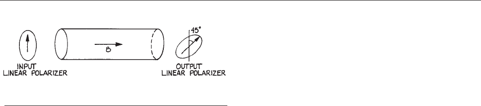
in Figure 4.64. Light passing in the reverse direction has
its plane of linear polarization also rotated by 45°,butin
a sense that makes it o rthogonal to the next polarizer so
negligible light emerges. Co mmercially available Fara-
day isolators typically provide 30 dB isolation and must
be selected for the specific wavelength desired. Both
free space a nd optical- fiber-based devices are available
from companies such as AC Photonics, Conoptics, Elec-
tro-Optics Tech nology, Isowave, Leysop, Linos Pho-
tonics, Namiki, New Focus, Newport, a nd OFR (now
Thorlabs).
Optical isolators are particularly useful in certain preci-
sion experiments using lasers, to avoid feedback instabil-
ity. If some of the light from a laser re-enters the laser, the
amplitude and phase of the laser will fluctuate, and this can
sometimes be very marked.
4.3.8 Filters
Filters are used to select a particular wavelength region from
light containing a broader range of wavelengths than is
desired. Thus, for example, they allow red light to be
obtained from a white light source, or they allow the isolation
of a particular sharp line from a lamp or laser in the presence
of other sharp lines or continuum emission. Although filters
do not have high resolving power (see Section 4.3.5), they
ha
ve much higher optical ef fi ciency at their operating wave-
length than higher-resolving-power, wavelength-selecti v e
instruments, such as prism or grating monochromators. That
is,theyhaveahighratiooftransmittedfluxtoinputfluxin
the wavelength region desired. Filters of several types are
av ailable for different applications.
Color Filters. A color filter selectively transmits a
particular spectral region while absorbing or reflecting
others. These simple filters are glasses or plastics
containing absorbing materials such as metal ions or
dyes, which have characteristic transmission spectra.
Such color filters are available from Chance-Pilkington,
Corning, CVI, Hoya, Kodak (Wratten filters), Kopp
Glass, Melles-Griot (now CVI-Melles-Griot), Newport,
Newport Thin Film Laboratory, Omega Optical,
Praezisions Glas & Optik, Schott, Rolyn, Rosco, and
Sterling Precision Optical. Transmission curves for these
filters are available from the manufacturers, and in
tabulations of physical and chemical data.
7,46
Care must be taken when color filters are being used to
block a strong light signal, such as a laser. These filters
may fluoresce, so although the primary incident light is
blocked, a weak, longer-wavelength fluorescence can
occur. We have seen this phenomenon quite strongly when
using orange plastic to block a blue/green laser.
Band-Pass Filters. A band-pass filter is usually a
Fabry–Perot etalon of small thickness. Although etalons
will be discussed in further detail in Section 4.7.4, a brief
discussion
is in order here.
In its simplest form, the Fabry–Perot etalon consists of a
plane, parallel-sided slab of optical material of refractive
index n and thickness d with air on both sides. In normal
incidence the device has maximum transmission for wave-
lengths for which the thickness of the device is an integral
number of half wavelengths. In this case, from Equation
(4.110):
Z
00
3
¼ Z
0
3
¼ Z
0
1
ð4:184Þ
and there is zero reflection. For incidence at angle h,regard-
less of the polarization state of the light, there is maximum
transmission for wavelengths (in vacuo) that satisfy:
mk
0
¼ 2d cos h
2
ð4:185Þ
where h
2
is the angle of refraction in the etalon.
A Fabry–Perot etalon is a ‘‘comb’’ filter. (Figure 4.159
shows an example of a transmission characteristic of such
a
device.) If the thickness of the etalon is small, the trans-
mission peaks are broad. In a typical band-pass filter oper-
ated as an etalon, all the transmission peaks but the desired
one can be suppressed by additional absorbing or multi-
layer reflective layers. The spectral width of the transmis-
sion peak of the filter can be reduced by stacking
Figure 4.64 Optical isolator that uses two linear polarizers
and a Faraday material producing a 45° polarization rotation.
212 OPTICAL SYSTEMS
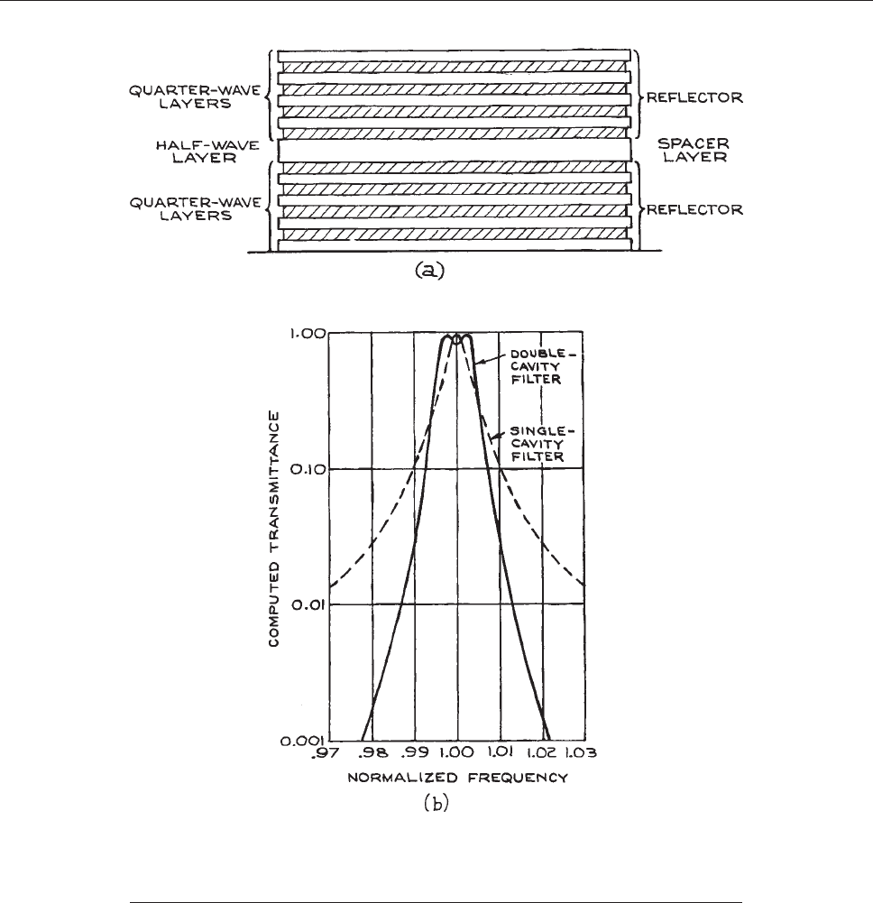
individual etalon filters in series. A single etalon filter
might consist, for example, of two multilayer reflective
stacks separated by a half-wavelength-thick layer, as
shown in Figure 4.65(a), while a two-etalon filter would
hav
e two half-wavelength-thick layers bounded by multi-
layer reflective stacks. Commercially available band-pass
filters for use in the visible usually have a passband ranging
from below 1 nm to 50 nm (full width at half maximum
Figure 4.65 (a) Construction of an all-dielectric single-cavity Fabry–Perot
interference filter; (b) theoretical transmittance characteristics of single- and
double-cavity filters. (From Handbook of Lasers, R. J. Pressley (Ed.), CRC Press, Cleveland,
1971; by permission of CRC Press, Inc.)
OPTICAL COMPONENTS 213
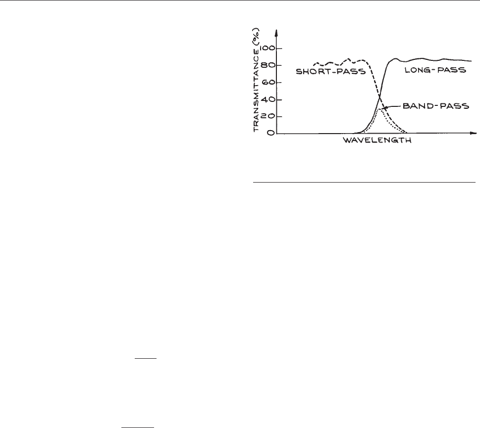
transmission). The narrowest band-pass filters are fre-
quently called ‘‘spike filters.’’ Filters to transmit particu-
lar wavelengths, such as 632.8 nm (He-Ne laser), 514.5
and 488 nm (argon ion laser), 404.7, 435.8, 546.1, 577.0, and
671.6 nm (mercury lamp), 589.3 nm (sodium lamp), and
other wavelengths, are available as standard items.
31
Fil-
ters at nonstandard wavelengths can be fabricated as cus-
tom items. Band-pass filters for use in the ultraviolet
usually have lower transmittance, typically 20%, than fil-
ters in the visible, whose transmittance usually ranges from
40% to 70%, being lowest for the narrowest passband.
Infrared band-pass filters are also readily obtained, at least
out to about 10 lm, and have good peak transmittance. The
typical available band-pass for a filter whose peak trans-
mission is k
peak
can usually be estimated as k
peak
/50,
although narrower band-pass filters can be obtained at
higher cost. Band-pass filters are available from many sup-
pliers, including Andover Optical, LOT-Oriel, Melles
Griot, Newport, Omega Optical, Spectrogon, Spectrum
Thin Films, and Sterling Precision Optical.
Band-pass filters are usually designed for use in normal
incidence. Their peak of transmission can be moved to shorter
wavelengths by tilting the filter, although the sharpness of the
transmission peak will be degraded by this procedure. If a
filter designed for peak wavelength k
0
is tilted by an angle
h, its transmission maximum will shift to a wav elength:
k
s
¼ k
0
ffiffiffiffiffiffiffiffiffiffiffiffiffiffiffiffiffiffiffi
1
sin
2
h
n
2
s
ð4:186Þ
where n is the refractive index of the half-wavelength-thick
layer of the filter. For small tilt angles:
k
0
k
s
¼
k
0
sin
2
h
2n
2
ð4:187Þ
Thus, a band-pass filter whose peak-transmission wave-
length is somewhat longer than desired can be optimized
by tilting.
Long- and Short-Wavelength-Pass Filters. A
long-wavelength-pass filter is one that transmits a broad
spectral region beyond a particular cutoff wavelength, k
min
.
A short-wavelength-pass filter transmits in a broad spectral
region below its cutof f wavelength k
max
. A combination of a
long-wavelength-pass and a short-wavelength-pass filter can
be used to produce a band-pass filter, as shown in Figure
4.6
6. Although long-and short-wavelength-pass filters usu-
al
ly involve multilayer dielectric stacks, the inherent
absorption and transmission characteristics of materials
can be utilized. Semiconductors exhibit fairly sharp long-
wavelength-pass behavior beginning at the band gap
energy. For example, germanium is a long-pass filter
with k
min
¼ 1.8 lm.
Holographic Notch Filters. These filters are special
diffractive structures that reflect a narrow range of wave-
lengths (~5 nm) very strongly, and consequently they
reduce transmitted light substantially (40–60 dB) over
the same narrow range. These filters are ideal for rejection
of laser light in experiments where a weaker light signal –
fluorescence or Raman scattering – is being studied, and
some scattering or reflection of the excitation laser light is
occuring. These filters are available from Andor Technol-
ogy, Del Mar Ventures, Kaiser Optical Systems, MK Pho-
tonics, and Semrock.
Rugate Filters. Rugate filters are notch interfe rence
filters with high rejection of a narrow band of
wavelengths. In con trast to conventio nal multilayer
dielectric interference filters, in which the refractive
index variation from layer to layer is a square wave,
rugate filters use a sin usoidally variable refractive index
throughout the oxide film layers. They can provide a
single notch band without harmonics, as shown in
Figure 4.66 Schematic transmission of long- and short-
pass optical filters showing the band-pass transmission
characteristics of the two in combination.
214 OPTICAL SYSTEMS
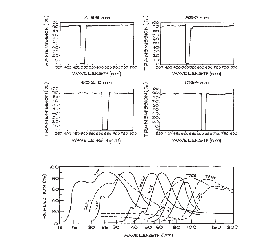
Figure 4.67. A rugate filter can look almost completely
colorless and transparent, and yet reject laser light at a
specified wavele ngth very efficiently. They are available
from Advanced Technology Coatings, Barr Associates,
Edmund Optics, Gist Optics, and Rugate Technologies.
Reststrahlen Filters. When ionic crystals are irradiated
in the infrared, they reflect strongly when their absorption
coefficient is high, and their refractive index changes
sharply. This high reflection results from resonance
between the applied infrared frequency and the natural
vibrational frequency of ions in the crystal lattice. The
characteristic reflected light from different crystals, termed
Reststrahlen, allows specific broad spectral regions to be
isolated by reflection from the appropriate crystal. Some
examples of Reststrahlen filters are given in Figure 4.68.
Christiansen Filters. In the far infrared, the alkali
halides exhibit anomalous dispersion: at certain
wavelengths their refractive indices pass through unity.
Figure 4.67 Transmission characteristics of some rugate filters.
Figure 4.68 Reststrahlen filters. (Courtesy of Harshaw Chemical Co.)
OPTICAL COMPONENTS 215
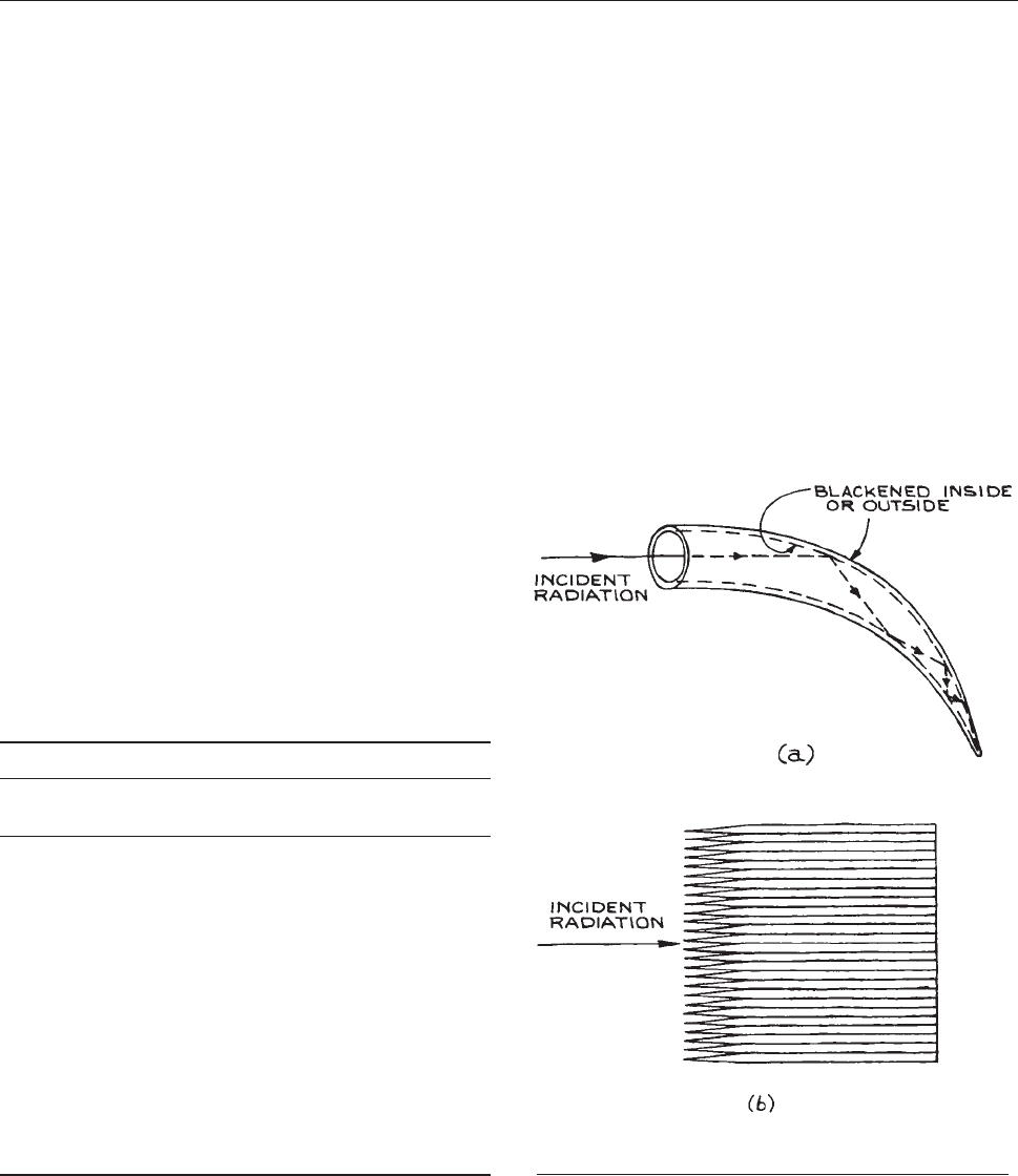
(Normal dispersion involves an increase of refractive index
with wavelength.) Thus a po wdered alkali halide, which
would generally attenuate a transmitted wave sev erely
because of scattering, will transmit well at wav elengths
where its refractiv e inde x is the same as that of air. Filters
using such an alkali halide powder held between parallel
plates are called Christiansen filters and provide sharp
transmission peaks at certain wav elengths listed in Table 4.4.
Neutral-Density Filters. Neutral-density (ND) filters
are designed to attenuate light uniformly over some broad
spectral region. The ideal neutral-density filter should have
a transmittance that is independent of wavelength. These
filters are usually made by depositing a thin metal layer on
a transparent substrate. The layer is kept sufficiently thin
that some light is transmitted through it. The optical
density D of a neutral-density filter is defined as:
D ¼ log
10
ð1=TÞð4:188Þ
where T is the transmittance of the filter. T is controlled
both by reflection from and by absorption in the metal
film. If such filters are stacked in series, the optical density
of the combination is the sum of the optical densities of
the individual filters, provided the filters are positioned so
that multiple reflection effects do not occur between them
in the direction of interest.
Neutral-density filters are used for calibrating optical
detectors and for attenuating strong light signals falling
on detectors to ensure that they respond linearly. Because
neutral-density filters usually reflect and transmit light,
they can be used as beamsplitters and beamcombiners
for any desired intensity ratio. There are many suppliers.
31
Variable ND filters are available from HB Optical, Melles
Griot, Nova Phase, Reynard, and Singh-Ray.
Light Traps. If a beam of light must be totally absorbed
(for example, in an application where any reflected light
from a surface could interfere with some underlying weak
emission), a light trap can be constructed. The two types
illustrated in Figure 4.69 work well: the Wood’s horn, in
Figure 4.69 Light traps: (a) Wood’s horn; (b) stacked razor
blades.
Table 4.4 Christiansen filters
Crystal Wavelength of Maximum
Transmission (lm)
LiF 11.2
NaCl 32
NaBr 37
KCl 37
RbCl 45
NaI 49
CsCl 50
KBr 52
CsBr 60
TlBr 64
KI 64
RbBr 65
RbI 73
TlI 90
216 OPTICAL SYSTEMS
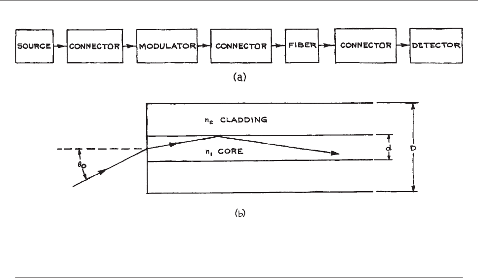
which a beam of light entering the trap is gradually
attenuated by a series of reflections at an absorbing
surface made in the form of a curved cone (usually made
of glass); and a stack of razor blades, which absorbs
incident light very efficiently.
4.3.9 Fiber Optics
As is well known, the use of o ptical fibers has become
widespread in the telecommunications field. Conse-
quently, there are numerous suppliers of the various
components and subsystems involved.
31
The use of
optical fibers in scientific research can be a very valua-
ble technique, and one that is not particularly compli-
cated. For example, in experiments where radio
frequency (rf) interference, pickup, and ground loops
are a problem, an experimental signal can be used to
modulate a small light-emitting diode or laser. The
modulated optical signal is then passed along an optical
fiber to the observation location, where the original elec-
trical signal can be recovered with a photodiode. Com-
plete analog transmission systems of this kind are
available from A.A. Lab Systems, Alcatel, Analog
Modules, Force, J DS Uniphase, Luxlink, and Metrotek
Industries. A schematic diagram of the various compo-
nents of such a system is shown in Figure 4.70(a).
The
source may be supplied fabricated directly onto a
fiber. The modulator is frequ ently unnec essary, as th e
source itself can be directly amplitude-modulated. The
detector may also be supplied fabricated directly onto
the end of the fiber. A f ew spec ific points are worthy of
note for the experimentalist who may wish to utilize this
technology.
For certain laboratory applications the construction of
a fiber system without any connectors is straightforward.
Light from the source is focused into the end of the fiber
with a microscope objective. Light emerging from the
other end of the fiber is focused onto the detector in a
Figure 4.70 (a) Fundamental components of a fiber-optic data link; (b) meridional section through a step-index optical
fiber. The core refractive index is n
1
; the cladding refractive index is n
2
. The core and cladding diameters are d and D,
respectively. A ray entering the fiber will be totally internally reflected provided its angle of incidence is less than h
0
, where
sin h
0
¼ NA.
OPTICAL COMPONENTS 217

similar way. A convenient range of microscope objec-
tives for this purpose is available from Newport, who
also supply a wide range of components for holding
and positioning fibers. The choice of lens focal length
and placement is governed by the numerical aperture
(NA) of the fiber. The meaning of this parame ter ca n
be understood with reference to Figure 4.70(b),which
sho
ws a merid ional section through a so-called step-
index fiber. In this composite fiber the cylindrical core
has re fractive index n
1
, and the surrounding c ladding has
index n
2
, where for total internal reflection of rays to
occur in the core, n
1
> n
2
. Light entering the fiber at
angles < h
o
will totally internally reflect inside the core.
The NA is:
sin h
o
¼
ffiffiffiffiffiffiffiffiffiffiffiffiffiffiffi
n
2
1
n
2
2
q
ð4:189Þ
Commercially available fibers typically have a
smoothly varying radial index profile, but the NA is
still the appropriate parameter for determining the
acceptance angle. Two specific types of fiber are in
most common use: single-mode and multimode. Sin-
gle-mode fibers typically have core diameters on the
order of 10 lm and cladding diamete rs of 125 lm.
They require very precise connectors and are only
needed in specialized experiments, for example in
high data rate optical communications, where the abil-
ity of the fiber to support only a single propagating
mode is important. Multimode fibers have larger core
diameters, from 50 lmtoabove1mm,andcladding
diameters somewhat larger than their respective core
diameters. These fibers are easy to use: the larger sizes
are frequently used to channel light for illumination
into pos itions that are difficult to access, or to collect
light from o ne location a nd channe l it to a detector
somewhere else. Large fibers that are suitable for these
purposes are available from AFL Telecommunications,
Berkshire Photonics, Edmund Optics, Fiberguide
Industries, Newport, P olymicro Technologies, and
3M Speciality Optical Fibers.
Fibers can be cut to provide a flat end face with the aid
of specialist cleaving tool s of varying degrees of preci-
sion and complexity, available from suppliers such as
Newport and York. In s imple experimental setups an
adequate cleaved flat face can be obtained in the follow-
ing way:
(1) Remove the outer plastic prot ect ive coating from
the cladding in the region that is to be cut by using
afiber-strippingtoolorbyimmersingthispartofthe
fiber in methylene chloride (the active ingredient in
most proprietary paint and varnish strippers). To
clean a fiber that has been stripped of its cladding
use Kimwipes or lens tissue moistened with pure iso-
propyl alcohol. Do not wipe the bare fiber with dry
tissue.
(2) Lightly scratch the cladding with a cleaving tool
(slightly more precise than a conventional glass cutter).
(3) Fasten one half of the fiber to a flat surface with mask-
ing tape, and pull the other half of the fiber axially
away, keeping the fiber flat on the surface.
This pro cedure usually g ives a flat eno ugh face for
use w ith a microscope obje ctive. If fibers are to be cut
and fitted with connectors, they must be cut and pol-
ished according to the instructions supplied with the
connector.
Fiber Optic Connectors. If two identical fibers are
to be joined together, this can be done with mechanical
coaxial connector s, with a mechanical splice, or the
fibers can be fused together with a fusion splicer. In all
cases the flat, cleaved faces of the two fibers to be joined
must be brought together so that the two faces are in
close proximity, are parallel, and the fibers are coaxial.
Proper alignments for orthogonal and angle c leaves are
shown in Figure 4.71(a) and (b) , respectively. Any
lateral
or tilt offset of the fibers when they are joined
will reduce coupling efficiency. Precision mechanical
optical fiber connectors are able to couple two fibers
together with losses in the range 0.1–0.2 dB.
Sometimes the connector contains a small amount of
index-matching gel that is squeezed in the gap
between the fibers.
Mechanical fiber s plices are an inexpensive way to
join fibers. They generally have a sleeve-like construc-
tion into which the two fibers ar e pushed and then
glued or clamped in place. Better yet, a fusion splicer
can be used to fuse fibers together; this is, however, an
expensive device. A good fusion splice can have a loss
218 OPTICAL SYSTEMS
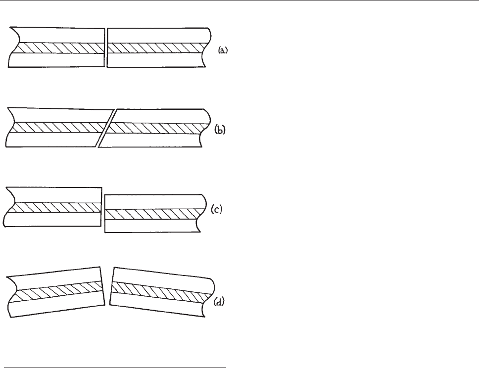
below 0.1 dB. After two fibers are f used together, a
splice protector should be included if the joined fiber
is to be protected from failure of the splice.
The use of optical fiber devices is much simplified
if these devices are purchased with appropriate fiber
optic connectors already attached. A convenient way
to obtain a connectorized fiber whe re access to one
free end is required is to buy a fiber jumper,which
is the optical equivalent of patch cord or coaxial
cable. By cutting the jumper cable, a length of fiber
with a conn ector on one end i s easily ob tained. Fiber
jumpers with various kinds of connectors, different
fiber optic cables, and of various lengths are readily
available (Cableorganizer.com, Datamax Technologies,
Fiberall, Fiber.com, Fiber Optic Cable Shop, L-Com,
Optica, Stonewall Cable, and Unicom). Fiber optic
connectors come in many types for both single-mode
and multimode fibers: FC, LC, SMA, ST, SC, MT-RJ ,
MU, 50/125, D4, E20 00, 62.5/1 25, 9/125, and O pto-
clips. For special applications, angle-cleaved connec-
tors are available, which reduce the inevitable small
reflection that occurs at a fiber connector. A c ompre-
hensive discussion of practical fiber optics can be
found in Goff.
47
Polarization-maintaining (PM) fiber will preserve the
polarization state of launched light (to about 1% purity).
Special connectors and splicing techniques are needed for
PM fiber, as the azimuthal orientation of the two fibers is
now important.
4.3.10 Precision Mechanical
Movement Systems
It is frequently necessary to be able to position compo-
nents in an optical system with high precision. The type
of stage with which this is done depends on the scale of
movement, the accuracy, repeatability resolution, and
freedom from backlash that is required. There a re a
large number of suppliers of stages, including transla-
tion, rotation, tilting, multi-ax is positioning and combi-
nations of these including Aerotech, Daedal, Melles
Griot, Newport, New Focus, Optosigma, Thor Labs,
and Velmex. Both manual and moto r-driven stages are
available. Although precision mechanica l stages can be
built in the laboratory, they are widely available com-
mercially. It is not likely that an experimentalist will
save money by building rather than buying a precision
stage.
The ac curacy of adjustment is the difference between
the actual and desired positions. Repeatability refers
to the ability to reproduce a desired position after a
movement of a stage to a different position. In a fair
comparison of stages this should involve significant,
comparable movements away from, and t hen back to
a desired position. Resolution is the smallest motion
that a stage can make , which for a screw-driven
device will be limited by factors such as the number
of threads per inch in the lead screw, and friction. A
Figure 4.71 Alignment of optical fibers for optical
connection: (a) correct alignment for perpendicular-cleaved
fibers; (b) correct alignment for angle-cleaved fibers;
(c) lateral misalignment; (d) angle misalignment.
OPTICAL COMPONENTS 219
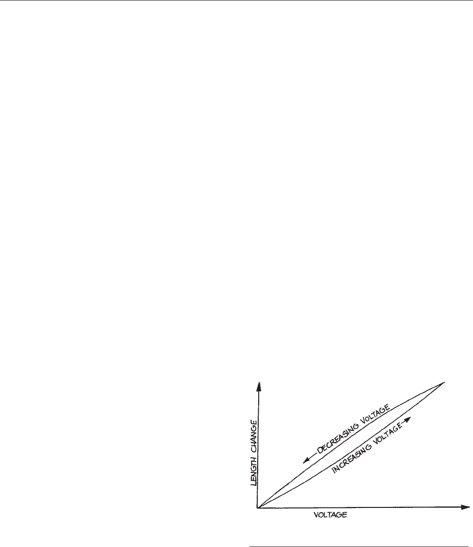
precision micromete r might, for example, have a reso-
lution of about 1/10 of the smallest scale graduation
around the micrometer head. Another factor of impor-
tance i s cree p. A fter a stage has b een set to a desired
position does it stay there, or does removal of stress from
a positioning screw c ause it to relax? Absence of creep
means that a mount, once positioned, holds its position
for a long period. It is our experience that stainless-steel
mounts are less sus ceptible to creep than aluminum
mounts.
Resolution alone as a specification does not mean
much without additional specification of accuracy, repeat-
ability, and stability. The long-term stability of a mount
is also influenced by the thermal stability and expansion
of the materials from which the stage is made. The con-
venient materials of construction are aluminum alloy and
stainless steel.
Aluminum has a higher coefficient of thermal expansion
(24 3 10
–6
/K) compared with stainless steel (10–16 3
10
–6
/K), but aluminum has a higher thermal conductivity
and reaches thermal equilibrium more quickly, which min-
imizes thermally induced strain. Aluminum takes a poor
thread and usually brass threaded inserts must be used for
brass or stainless-steel positioning screws.
The thermal stability of an optical mount can be
improved by using mounting assemblies constructed with
two dissimilar metals whose thermal expansions offset
each other. Commercially available mounts of the highest
precision may include this technology. The manufacturer’s
technical specifications should be consulted.
It is convenient to divide the movement scales available
into three broad categories.
(1) Medium – the scale of movement provided by manual
micrometer drives or precision lead screws. Typical
micrometer drives provide up to 50 mm travel with
accuracy on the order of 1 lm. Some commercial
drives claim a resolution below 0.1 lm, but, in prac-
tice, such claims must be reviewed with skepticism,
since the backlash, creep and repeatability of all
mechanical, screw-based, stages is likely to be worse
than this.
(2) Fine – The scales of movement, precision, and
repeatabily provided by motor-driven stages, which
may be driven either by a stepping motor or dc
motor. For repeatability, some form of encoding of
the position is needed, or feedback based o n the
characteristics of the state. Position encoding is usu-
ally done with either a shaft encoder, which tells
the drive motor on the lead screw exactly what its
angular position is, or with a linear encoder. A
linear encoder gives a more prec ise, r epeatable
measure of the actual location of the object being
moved. Precision drives incorporating encoders are
available from Griffin Motion, Newport, Physik
Instrumente (PI), Quater, a nd Thorlabs. Precise
motor-driven stages are also available from Aerotech,
J.A. Noll, Daedal, Melles-Griot, Newport, and New
Focus.
(3) Nanoscale – p ositioning down to 1 nm resolution,
with varying degrees of repeatability. Positioning on
this scale requires the use of piezoelectric or electro-
static transducers. Piezoelectric transduc ers ge ner-
ally use a ceramic ma terial such as lead zirconate
titanate (PZT), which changes its shape in an
applied electric field. Typical PZT transducers pro-
vide me chanical motion on the orde r of a few hun-
dreds o f nanometers for applied voltages on the
order of 1 kV. They provide resolution of 10 nm or
less, but do exhibit hysteresis, as shown i n Figure
4.
72, unless some absolute position encoding
sch
eme is used. Individual PZT transduc ers are gen-
erally available either in the form of tubes or disks,
Figure 4.72 Hysteresis in the length change of
a piezoelectric element with applied voltage.
220 OPTICAL SYSTEMS
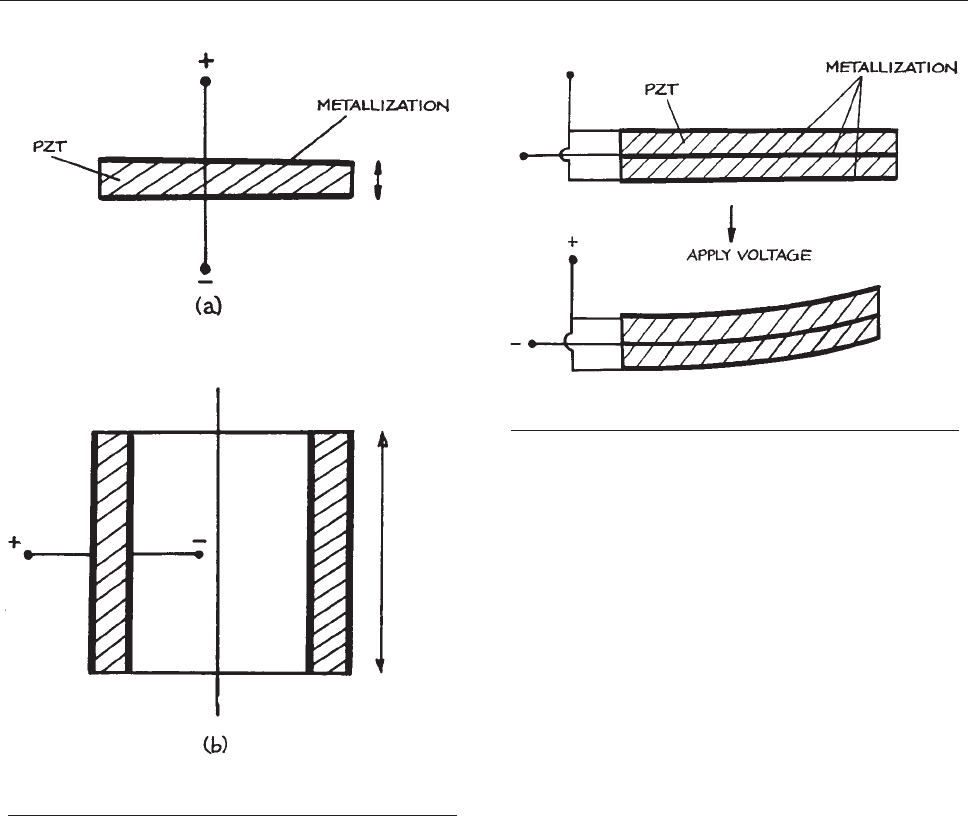
as shown in Figure 4.73 . Larger motions can be
obtained by stacking transducers in either a bimorph
or p olymorph arrangement. In a bimorph, two slabs
of PZT are driven so that one slab extends while the
other gets shorter, which ca uses the bimorp h to
bend, as shown in Figure 4.74.
In
a slab transducer, voltage is applied across the narrow
dimension of the slab, which will then change its thickness
with applied voltage. In a cylindrical transducer, voltage is
applied between the inner and outer metallized cylindrical
surface of the tube, which then changes its length in the
axial direction. Nanoscale precision piezoelectric drives
are available commercially from Attocube, Mad City
Labs, Melles Griot, Queensgate Instruments, Polytec,
Physik Instrumente, and Thorlabs, among others.
Bimorphs are available from FDK Products and Morgan
Electro Ceramics.
Small scale (~10 lm) precision motion in each of
three orthogonal axes can be accomplished inexpen-
sively with a mo dified piezotube. A typical piezotube
is on the order of 30 mm long by 10 mm, and is generally
supplied with a metal coating on its inner and outer
cylindrical surfaces. The outer metallization should be
removedinfoursegementsapproximately1mmwide
spaced 90° apart on the outer cylindrical surface, as
shown in Figure 4.75. The four segements are then
d
riven by a ‘‘bridge’’ amplifier current, in which oppo-
site pairs of electrodes are driven in a push-pull config-
uration, as shown schematically in Figure 4.76.Driving
e
lectrodes 1 and 2 produces an x-directed tilt of the tube,
electrodes 3 a nd 4 produce a y-directed tilt of the tube.
An additional amplifier drives electrode 5 for z-directed
extension of the tube. Because the interelectrode
Figure 4.74 Operation of a bimorph piezoelectric element
in a parallel configuration.
Figure 4.73 Simple piezoelectric elements: (a) slab; (b)
cylinder.
OPTICAL COMPONENTS 221
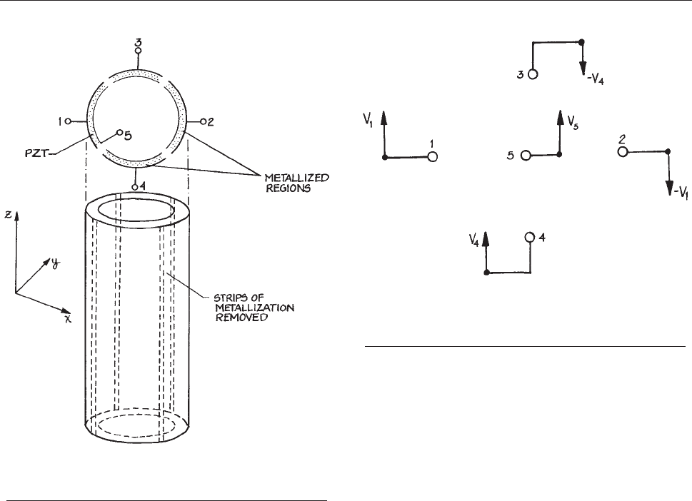
voltages used need to be as large as 1000 V, special op-
amps are required. Approp riate amplifers a re available
from Apex Microtec hnology Corporation. Piez o tubes
are available from Argillon, APC International, Boston
Piezo-Optics, Omega Pie zo Technologies, Physik
Instrumente (PI), and Sensor Technology.
4.3.11 Devices for Positional and
Orientational Adjustment of
Optical Components
For positioning a given component, the maximum number
of possible adjustments is six: translation along three
mutually orthogonal axes and rotation about these (or
other) axes. Mounts can be made that provide all six of
these adjustments simultaneously. Usually, however, they
are restricted and have no more degrees of freedom than
are necessary. Thus, for example, a translation stage is
usually designed for motion in only one dimension; inde-
pendent motion along other axes can then be obtained by
stacking one-dimensional translation stages. Orientation
stages are usually designed for rotation about one axis
(polar rotation) or two orthogonal axes (mirror mounts or
tilt tables). Once again, such mounts can be stacked to
provide additional degrees of freedom. It is often unneces-
sary for angular adjustment to take place about axes that
correspond to translation directions.
The ideal op tical mount provides independent
adjustment in each of its degrees of freedom without
any interaction with other potential degrees of free-
dom. It should be sturdy, insensitive to extraneous
vibrational disturbances, (such as air- or structure-
borne acoustic vibrations), and free of backlash during
adjustment. Generally it should be designed on k ine-
matic principles (see Section 1.7.1). The effect of tem-
perature
variations on an optical mount can also be
reduced, if desired, by constructing the mount from
Figure 4.76 Voltage drive scheme for a piezoelectric
element such as the one shown in Figure (4.69). Electrodes
1–4 are the quadrant electrodes, Electrode 5 is the inner
electrode.
Figure 4.75 A cylindical piezoelectric element with outer
quadrant electrodes. The element can be driven to provide
axial motion as well as tilt in two orthogonal axes.
222 OPTICAL SYSTEMS
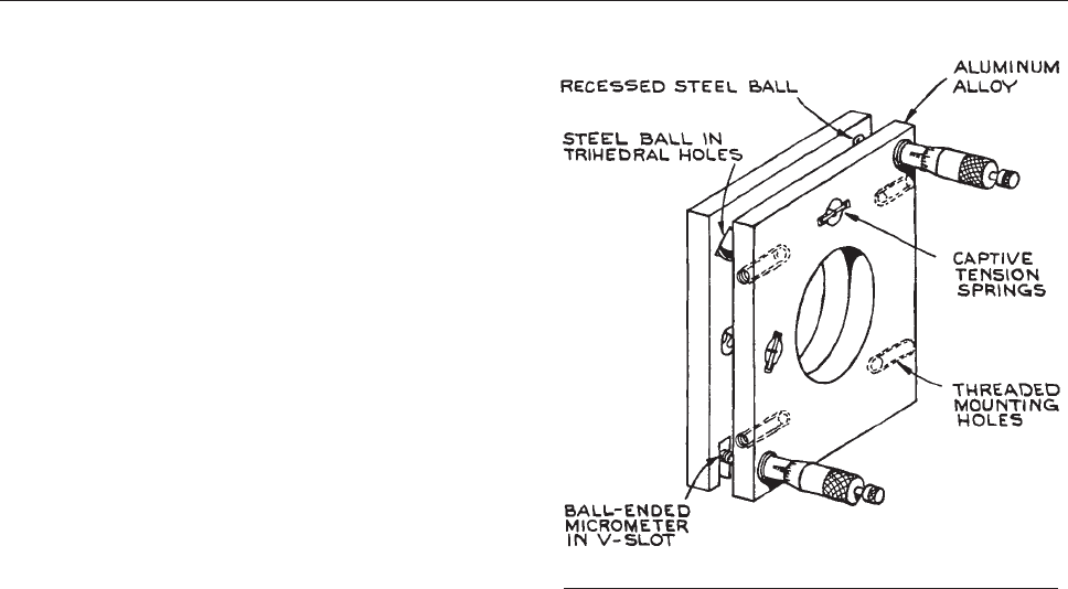
low-coefficient-of-expansion material, such as Invar, or
by using thermal-expansion compensation techniques.
Very high ridigity in an optical mount generally implies
massive construction. When weight is a limitation,
honeycombed material or material appropriately
machined to reduce excess weight can be used. Most
commercially available mounts are not excessively
massive, but represent a compromise between size,
weight, and rigidity. Generally, mounts do not need to
be made any more rigid than mechanical considerations
involving Young’s modulus and likely a pplied forces
on the mount would dictate.
The design of optical mounts on kinematic principles
involves constraining the mount just enough so that, once
adjusted, it has no degrees of freedom. Some examples
will illustrate how kinematic design is applied to optical
mounts.
Two-Axis Rotators. Within this category the
commonest devices are adjustable mirror or grating
mounts and tilt tables used for orienting components
such as prisms. Devices that adjust orientation n ear the
horizontal are usually called tilt adjusters. Mirror
holders, on the other hand, involve adjustment about
a vertical or near-vertical axis. A basic device of either
kind involves a fixed stage equipped with three spherical
or hemispherical ball bearings, which locate,
respectively, in a V-groove, in a conical hole, and on a
plane surface machined on a movable stage. A typical
device is shown in Figure 4.77. The movable stage
makes
contact with the three balls on the fixed stage at
just six points – sufficient to prevent motion in its six
degrees of freedom – and is held in place with tension
springs between the fixed and movable stages.
Adjustment is provided by making two of the locating
balls the ends of fine-thread screws or micrometer heads.
Suitable micrometer heads for this purpose are
manufactured by Brown a nd Sharpe, Mitutoyo, Moore
and Wright, Shardlow, and Starrett, and are available
from most wholesale machine-tool suppliers. The ball
of the micrometer should be very accurately centered on
the spindle. The adju stment of the mo unt shown in
Figure 4.77 is about two almost orthogonal axes.
Th
ere is s ome transla tion of the center of the movable
stage du ring ang ular adjustment, which can be avoided
by the use of a true gimbal mount.
A few of the constructional details of the mount in
Figure 4.77 are worthy of note. Stainless steel, brass,
and
aluminum are all suitable materials of construction;
an attempt to reduce the thermal expansion of the
mount by machining it from a low-expansion material
such as Invar may not meet with succe ss. Extensive
machining of low-expansion-coefficient alloys gener-
ally increases the coefficient, unless they are carefully
annealed afterward. Puttin g the component in boiling
water and letting it gradually cool will lead to partial
annealing. True kinematic design requires ball location
in a trihedr al hole, in a V-slot, a nd on a p lane surface
(or in three V-slo ts, but this no longer permits angular
adjustment about orthogona l axes) (see also Section
1.
7.1). If the mount is made of aluminum, the locating
hole,
slot, and plane on the movable stage should be
made of stainless steel, or s ome other hard material,
shrunk-fit into the main aluminum body. A true trihe-
dral slot can be made with a punch, as shown in
Figure 4.77 Kinematic double-hinge mirror mount.
OPTICAL COMPONENTS 223
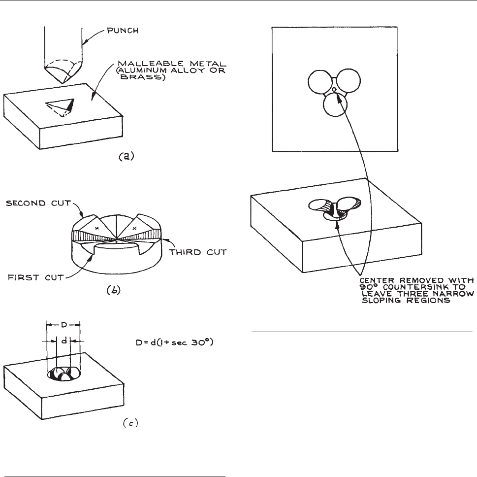
Figure 4.78(a), or it can be machined with a 45° milling
cutter as shown in Figure 4. 78(b). A co nical hole i s not
t
ruly kinematic; a compromise design is shown in
Figure 4.79.
Altho
ugh motion of the mount in Figure 4.77 results
fr
om direct micrometer adju stmen t, various c ommerc ial
mounts incorporate a reduc tion mechanism to increase
the s ensitivity of the mount. Typical schemes that are
used involve adjustment of a wedge-shaped surfac e by a
moving ball, as shown in Figure 4.80,ortheuseofa
d
ifferential screw drive . The two or more movable stages
of an adjustable mount can be held together with captive
tension springs, as in Figure 4.77. Designs involving only
small
angular adjustment can utilize the bending of a thin
section of material, as shown in Figure 4.81. The design of
such
mounts, called flexures, is discussed in detail in
Section 1.7.6.
The
basic principle of a gimbal mount for two-axis
adjustment is shown in Figure 4.82. True orthogonal
motion
about two axes can be obtained in such a design
Figure 4.79 Compromise design for kinematic trihedral
hole.
Figure 4.78 Methods for making trihedral locating holes
for kinematic design; (a) trihedral steel punch; (b) trihedral
hollow machined with 45° milling tool; (c) steel balls fitting
tightly in a hole.
224 OPTICAL SYSTEMS
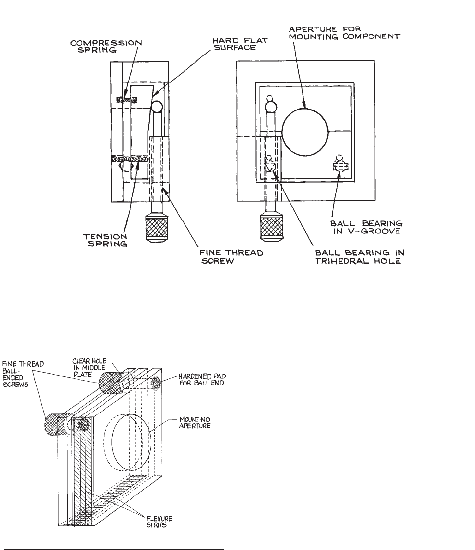
without translation of the center of the adjusted compo-
nent. A kinematically designed gimbal mount is, however,
much more complicated in construction than the mount
shown in Figure 4.82. Precision gimbal mounts should
be
purchased rather than built. Very many companies man-
ufacture adequate devices with a variety of designs, and
their prices are lower than the cost of duplicating such
devices in the laboratory. Suppliers of gimbal mounts in-
clude Aerotech, Daedal, New Focus, Newport, J. A. Noll,
Standa, and Thorlabs. Most of these manufacturers also
manufacture good nongimbal mounts similar to the one
shown in Figure 4.77.
Translation Stages. Translation stages are generally
designed to provide linear motion in a single dimensio n
and can be stacked to provide additional degrees of free-
dom. Mounts fo r centering optical components, particu-
larly lenses, incorpor ate motion in two orthogonal (or
Figure 4.80 Cutaway views of a kinematic, single-axis rotator incorporating a
reduction mechanism involving a ball bearing on an angled surface. Two rotators of
this kind could be incorporated in a single mount to give two-axis gimbal adjustment.
Figure 4.81 Flexure type double-hinge mirror design.
OPTICAL COMPONENTS 225
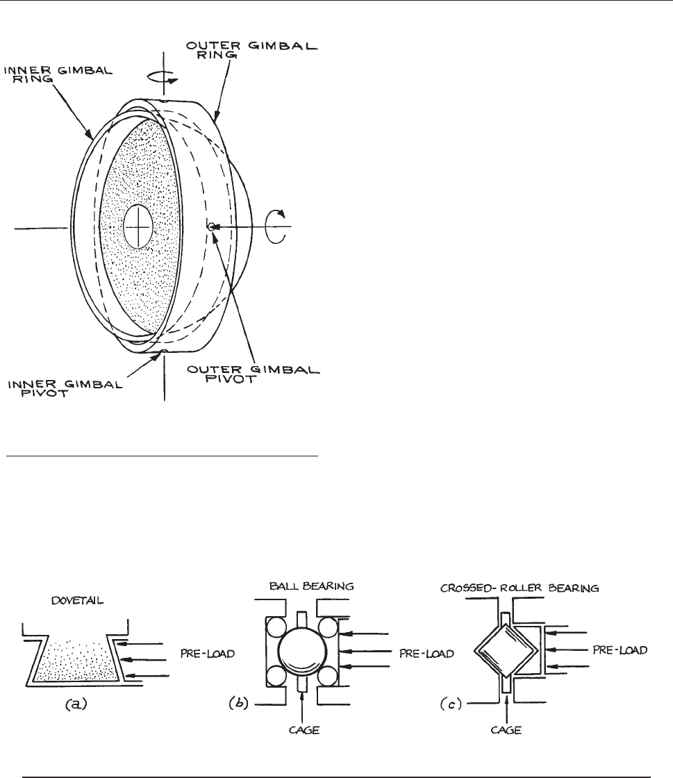
near-or thogonal) axes in a single mount. The simplest
translation stages usu ally involve some sort of dovetail
groove arrangement, as shown in Figure 4.83(a).Greater
pr
ecision can be obtained with ball bearings captured
between V-grooves with an arrangement to prevent adja-
cent balls from touching, as shown in Figure 4.83(b),or
w
ith crossed-roller bearings, as shown in Figure 4.83(c).A
simple
ball-bearing groove design is shown in Figure 4.84,
although
variants are possible. Suppliers of precision,
roller bearing translators include Aerotech, Daedal,
Melles Griot, Newport, OptoSigma, and Thorlabs. Vertical
translators using a fine-thread screw drive are available
from Newport. Stages can be built to provide short-range,
highly stable, frictionless precision movement by using
flexures, as shown in Figure 4.85. Typical travel of a flex-
ure
stage is on the order of 10% to 15% of the dimensions
of the stage.
Less precise, but generally adequate, nonball-bearing
translation stages are available from Newport and Velmex.
Mounts for centering optical components such as lenses
are available from Aerotech, Ealing, and Newport, among
others. A simple kinematic design for a centering mount is
illustrated in Figure 4.86.
Rotators and Other Mounts. Rotators are used, for
example, for orienting polarizers, retardation plates,
prisms, and crystals. They provide rotation about a single
axis. Precision devices using ball bearings are available
from Aerotech, New Focus, Newport, OptoSigma, and
Thorlabs, among various other suppliers.
There are numerous more complicated optical mounts
than those described in the previous sections, which pro-
vide in a single mount any combination of degrees of free-
dom desired. Motor-driven and computer-controllable
versions of all these mounts are generally available. For
Figure 4.82 Schematic diagram of a true two-axis gimbal
mount. The center of the mounted component does not
translate during rotation.
Figure 4.83 Groove mounting arrangements for linear transation stages: (a) dovetail V-groove; (b) ball bearing;
(c) crossed-roller bearing.
226 OPTICAL SYSTEMS
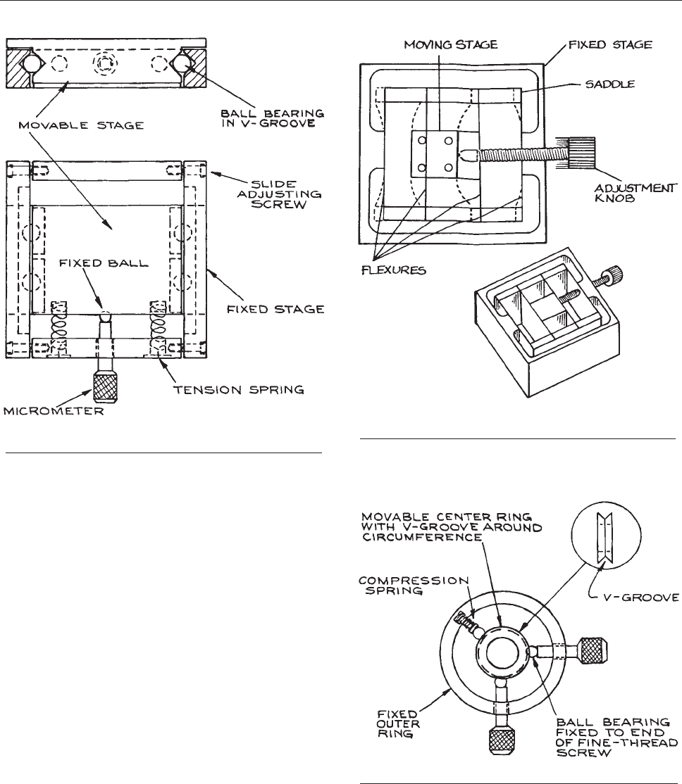
details, the catalogs of the manufacturers previously men-
tioned should be consulted.
Optical Benches and Components. For optical
experiments that involve the use of one or more
optical compo nents in conjunctio n with a sou rce and/
or a detector in some sort of linear optical
arrangement, construction usin g an o ptical bench and
components is very convenient, particularly in
breadboarding applica tions. The commonest such
bench d esign is base d on the equilateral triangular bar
developed by Zeiss and typically machined from lengths
of stabilized cast iron. Aluminum benches of this type
are a lso available, but are less rigid. Components are
mounted on the bench in r od-mounted holders t hat fit
into carriers that locate on the triangular ben ch. A cross-
sectional diagram of a typical bench and carrier is shown
in Figure 4.87.
Figure 4.84 Section drawings of a simple 1-D translation
stage.
Figure 4.85 Linear translation stage using flexure
mounts.
Figure 4.86 A simple precision centering stage.
OPTICAL COMPONENTS 227
Coarse adjustment along the length of the bench is pro-
vided by moving the carrier manually. On many benches
this is accomplished with a rack-and-pinion arrangement. A
wide range of mounts and accessories are available, provid-
ing for vertical, lateral, and longitudinal adjustment of
mounted-component positions. Holders for filters, for cen-
tering lenses, and for holding and rotating prisms and polar-
izers are readily obtained. Precision gimbal mounts,
translators, and rotators can be readily incorporated into
the structure. Examples of devices that lend themselves well
to optical-bench construction are telescopes, collimators,
laser-beam expanders and spatial filters, optical isolators,
and electro-optic light modulators. Optical benches and
accessories are available from Edmund Optics, Lasico, Linos
Photonics, Melles Griot, and Ne wport. Optical benches are
no longer as commonly used or available as they once were
because of the wide availability of optical tables and mounts,
and the additional flexibility provided by their use.
Piezoelectric Transducers. Most PZTs are made
from ferroelectric ceramics, such as lead zirconate titanate
or barium titanate, but polymers such as polyvinylidene
fluoride (PVF) are also used. Simple ceramic transducers
are usually supplied as flat discs with a metalized layer on
each flat face, or as short hollow cylinders, in which case
the metalized electrodes are deposited on the inner and
outer cylindrical surfaces. The flat discs change their thick-
ness with applied voltage, the cylindrical types change
their axial length. Typical length changes are on the order
of 10
–9
mV. Therefore, these devices are particularly suit-
able for very fine (submicron) positioning. Much larger
motions can be obtained with bimorph PZTs. Bimorphs
can be stacked to provide macroscopic motions for modest
applied voltages. Excursions of several millimeters can be
obtained for voltages of 1 kV. Even larger motions can be
obtained with Inchworm transducers, available from
EXFO-Burleigh and Sensor Technology. Basic ceramic
transducer elements are available from EDO Electro-
Ceramic Products, Physik Instrumente (PI), Piezo Sys-
tems, CTS Piezoelectric Products, Polytec, and Queen-
sgate Instruments. PVF transducers are available from
Atochem North America (formerly Pennwalt). Complete
transducer assemblies are available from EXFO-Burleigh,
Newport/Klinger, and Polytec Optronics.
Voice Coil Actuators. Voice coil actuators are a con-
venient way to generate linear movement in the range
between micrometers and tens of millimeters, with zero
hysteresis, and up to audio frequencies. They are essen-
tially the same as the mechanism in a loudspeaker that
moves the diaphragm to generate sound. They are direct
drive linear actuators that incorporate magnets and an elec-
trical coil. The voice coil itself is a noncommutated, two-
terminal device. It has linear control characteristics, zero
hysteresis, zero backlash, and infinite position sensitivity.
It has short mechanical and electrical time constants and a
high output power-to-weight ratio. A voice coil is gener-
ally operated in a control loop where a control signal is
provided from a position readout device. Voice coil
Figure 4.87 Typical dimensions of a Zeiss triangular optical
bench with carrier and mounted optical component.
(Courtesy of Ealing Corporation).
228 OPTICAL SYSTEMS

actuators are available from Airex, BEI Kimco, Equipment
Solutions, H2W Technologies, Innotics, and Orlin.
4.3.12 Optical Tables and
Vibration Isolation
A commercially made optical table provides the perfect
base for construction of an optical system. Such tables
have tops made of granite, steel, Invar, Superinvar (very
expensive), or ferromagnetic or nonmagnetic stainless
steel. When vibrational isolation of the table top is
required, the top is mounted on pneumatic legs. Such an
arrangement effectively isolates the table top from floor
vibrations above a few Hertz. To minimize acoustically
driven vibrations of the table top itself, the better metal
ones employ a laminated construction with a corrugated or
honeycomb metal cellular core bonded with epoxy to the
top and bottom table surfaces.
Granite table tops are very much less intrinsically reso-
nant than metal tops and represent the ultimate in dimen-
sional stability and freedom from undesirable vibrational
modes. Complete pneumatically isolated optical table sys-
tems, nonisolated tables, and table tops alone are available
from Kinetic Systems, Melles Griot, Newport, Standa,
Thorlabs, and TMC. In selecting a table, points of compar-
ison to look for include the following:
(1) The overall flatness of the table top (flatness within
50 lm is good, although greater flatness can be obtained)
(2) The low-frequency vibration isolation characteristics
of the pneumatic legs
(3) The rigidity of the table top (how much it deforms with
an applied load at the center or end)
(4) The isolation from both vertical and horizontal vibra-
tions
(5) The frequencies and damping of the intrinsic vibra-
tional modes
(6) Are the threaded holes in the table top sealed so that
liquid spills do not disappear into the interior honey-
combs of the table?
Other criteria, such as cost and table weight, may be
important. Typical sizes of readily available tops range
up to 5 3 12 ft (larger tables are also available) and in
thickness from 8 in. to 2 ft. The thicker the table, the
greater its rigidity and stability. Most commercial tables
are available with 1= 4-20 threaded holes spaced on 1 in.
centers over the surface of the table. Better designs use
blind holes of this type so that liquids spilt on the table
do not vanish into its interior. Ferromagnetic table tops
permit the use of magnetic hold-down bases for mounting
optical components. Such mounts are available from
numerous optical suppliers. It is cheaper, and just as sat-
isfactory, to buy magnetic bases designed for machine-tool
use from a machine-tool supply company.
Steel and granite surface plates that can be used as
small, nonisolated optical tables are available from
machine-tool supply companies. If it is desired to construct
a vibration-isolated table in the laboratory, a 2 in. thick
aluminum plate resting on underinflated automobile-tire
inner tubes works rather well, although the plate will have
resonant frequencies. Very flat aluminum plate, called jig
plate, can be obtained for this application at a cost not
much greater than ordinary aluminum plate. Just mounting
a heavy plate on dense polyurethane foam also works sur-
prisingly well. In fact, the vibrational isolation of a small
optical arrangement built on an aluminum plate and
mounted on a commercial optical table is increased by
having a layer of thick foam between plate and table top.
Even the best-constructed precision optical arrangement
on a pneumatic isolation table is subject to airborne acous-
tic disturbances. A very satisfactory solution to this prob-
lem is to surround the system with a wooden particle-board
box lined with acoustic absorber. Excellent absorber mate-
rial, a foam–lead–foam–lead–foam sandwich called Hush-
cloth DS, is available from American Acoustical Products.
4.3.13 Alignment of Optical Systems
Small helium–neon lasers are now so widely available and
inexpensive that they must be regarded as the universal tool
for the alignment of optical systems. Complex systems of
lenses, mirrors, beamsplitters, and so on can be readily
aligned with the aid of such a laser: even visible-opaque
infrared components can be aligned in this way by the use
of reflections from their surfaces. Fabry–Perot interferom-
eters, perhaps the optical instruments most difficult to align,
are easily aligned with the aid of a laser. The laser beam is
shone orthogonally through the first mirror of the interfer-
ometer (easily accomplished by observing part of the laser
OPTICAL COMPONENTS 229
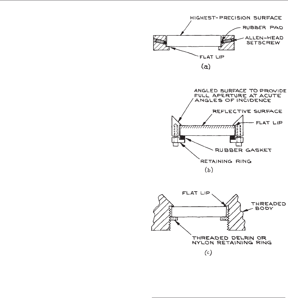
beam reflect back on itself), and the second interferometer
mirror is adjusted until the resultant multiple-spot pattern
between the mirrors coalesces into one spot.
4.3.14 Mounting Optical Components
A very wide range of optical devices and systems can be
constructed using commercially available mounts
designed to hold prisms, lenses, windows, mirrors, light
sources, and detectors. Some commercially made optical
mounts merely hold the component without allowing pre-
cision adjustment of its position. Many of the rod-mounted
lens, mirror, and prism holders designed for use with stand-
ard optical benches fall into this category, although they
generally have some degree of coarse adjustability; how-
ever, a wide range of commercially available optical mounts
allow precision adjustment of the mounted component.
The construction of a complete optical system from
commercial mounts can be very expensive, while provid-
ing in many cases unnecessary, and consequently undesir-
able, degrees of freedom in the adjustment and orientation
of the various components of the system. Although extra
adjustability is often desirable when an optical system is in
the ‘‘breadboard’’ stage, in the final version of the system it
reduces overall stability. An adjustable mount can never
provide the stability of a fixed mount of comparable size
and mass. Stability in the mounting of optical components
is particularly important in the construction of precision
optical systems for use, for example, in interferometry and
holography.
A custom-made optical mount must allow the insertion
and stable retention of the optical component without dam-
age to the component, which is usually made of some
fragile (glassy or single-crystal) material. If possible, the
precision surface or surfaces of the component should not
contact any part of the mount. The component should be
clamped securely against a rigid surface of the mount. It
should not be clamped between two rigid metal parts:
thermal expansion or contraction of the metal may crack
the component or loosen it. The clamping force should be
applied by an intermediary rubber pad or ring. Some exam-
ples of how circular mirrors or windows can be mounted in
this way are shown in Figure 4.88. If a precision polished
surface
of the component must contact part of the mount
(for example, when a precision lens, window, mirror, or
prism is forming a vacuum-tight seal), the metal surface
should be finely machined: the edges of the mounting sur-
face must be free of burrs. Ideally, the metal with which the
component is in contact should have a lower hardness than
Figure 4.88 Ways for mounting delicate optical compo-
nents: (a) no contact between precision surface of compo-
nent and mount; (b) precision surface in minimal contact
with mount and held in place with retaining ring; (c) pre-
cision surface in minimal contact with bottom of recess in
mount and held in place with threaded plastic ring.
230 OPTICAL SYSTEMS
the component. A thin piece of paper placed between the
component and metal will protect the surface of the com-
ponent without significantly detracting from the rigidity of
the mounting.
Generally speaking, unless an optical component has
one of a few standard shapes and sizes, it will not fit
directly in a commercial mount and a custom adaptor will
need to be made.
It is often necessary to mount a precision optical com-
ponent (usually a flat window or mirror, but occasionally a
lens or spherical mirror) so that it provides a vacuum- or
pressure-tight seal. There are two important questions to
be asked when this is done: can the component, of a certain
clear aperture and thickness, withstand the pressure differ-
ential to which it will be subjected, and will it be distorted
optically either by this pressure differential or the clamp-
ing forces holding it in place?
There are various ways of mounting a circular window
so that it makes a vacuum- or pressure-tight seal.
Demountable seals are generally made by the use of rub-
ber O-rings (see Section 3.5.2) for vacuum, or flat rubber
ga
skets for pressure. More-or-less permanent seals are
made with the use of epoxy resin, by running a molten
bead of silver chloride around the circumference of the
window where it sits on a metal flange , or in cert ain cases
by directly soldering or fusing the window in place. Some
crystalline materials, such as germanium, can be soldered
to metal; many others can be soldered with indium if they,
and the part to which they are to be atta ched , are appro-
priately treated with gold paint beforehand.
48
If a window
is fused in place, its c oefficient of expansion must be w ell
matched to that of the part to which it i s fixed. Suitably
matched glass, fused silica, and sapphire windows on
metal are available. Either the glass and metal are them-
selves matched, or an intermediate graded seal is used
(see Section 2.2.4). To decide what thicknes s-t o-un sup-
por
ted-diameter ratio is appropriate for a given pressure
differential, it must be determined whether the method of
mounting corresponds to Figure 4.89(a) or (b). In either
case,
the maximum stress in the window must be kept
below the modulus of rupture Y of the window by an
appropriate safety factor S
f
. A safety factor of four is
generally adequate for determining a safe window
thickness, but a larger factor may be necessary to avoid
deformationofthewindowthatwouldleadtodistortion
of transmitted wavef ronts. The desired thickness-to-free-
diameter ratio for a pressure differential p is found from
the formula:
t
D
¼
ffiffiffiffiffiffiffiffiffiffi
KpS
f
4Y
r
ð4:190Þ
where K is a constant whose value can be taken as 0.75
for a clamped edge and 1.125 for a free edge (see also
Sections 1.6.3 and 3.6.3).
A
window mounted with an O-ring in a groove, as shown
in Figure 4.90, may not provide an adequate seal at mod-
erately
high pressures, say above 7MPa
h
, unless the clamp-
ing force of the window on the ring is great enough to
prevent the pressure differential deforming the ring in its
grooves and creating a leak. A better design for high-pres-
sure use, up to about 50MPa, is shown in Figure 4.90(b):
the
clamping force and internal pressure act in concert
to compress the ring into position. Clamping an optical-
quality window or an O-ring seal of the sort shown in
Figure 4.90(a) may cause slight bending of the window.
If
an optical window has been fixed ‘‘permanently’’ in
place with epoxy resin, it may be possible to recover the
window, if it is made of a robust material, by heating the
seal to a few hundred degrees or by soaking it in methylene
chloride or a similar commercial epoxy remover.
49
If optical windows are to be used in pressure cells where
there is a pressure differential of more than 500 bars
(’ 7000 psi), O-rings are no longer adequate and special
window-mounting techniques for very high pressures must
be used.
50–52
Optical cells for use at pressures up to 3 kbar
are available from ISS, Inc.
Figure 4.89 Window mounting arrangements: (a) clamped
or fixed edge (maximum stress at edge); (b) unclamped or
freely supported edge (maximum stress at center).
OPTICAL COMPONENTS 231
4.3.15 Cleaning Optical Components
It is always desirable for the components of an optical sys-
tem to be clean. At the very least, particles of dust on mirrors,
lenses, and windows increase scattering; organic films lead
to unnecessary absorption, possible distortion of transmitted
wavefronts, and – in experiments with ultraviolet light sour -
ces – possible unwanted fluorescence. In optical systems
employing lasers, dust and films will frequently lead to visi-
ble, undesirable interference and diffraction effects. At
worst, dirty optical components exposed to high-intensity
laser beams can be permanently damaged, as absorbing dust
and films can be burnt into the surface of the component.
The method used for cleaning optical components, such as
mirrors, lenses, windows, prisms, and crystals, will depend
on the nature of both the optical component and the type of
contaminant to be removed. For components made of hard
materials, such as borosilicate glass, sapphire, quartz, or
fused silica, gross amounts of contamination can be
removed by cleaning in an ultrasonic tank. The tank should
be filled with water and the components to be cleaned
placed in a suitable pure solvent, such as acetone or tri-
chloroethylene, contained in a clean glass or plastic
beaker. If trichloroethylene is used, the operation should
be performed inside a fume hood because there is evidence
that this solvent is a human carcinogen. The ultrasonic
cleaning is accomplished by placing the beaker in the tank
of water. Dust can be removed from the surface of hard
materials, including most modern hard dielectric reflecting
and antireflecting coatings, by brushing with a soft camels-
hair brush. Suitable brushes are available from most photo-
graphic stores. Lens tissue and solvent can be used to clean
contaminants from both hard and medium-hard surfaces,
provided the correct method is used. The category of
medium-hard materials includes materials such as arsenic
trisulfide, silicon, germanium, gallium arsenide, KRS-5,
and tellurium. Information about the relative hardness of
these and other materials is contained in Table 4.5. Dust
should
first be removed from the component by wiping,
very gently, in one direction only, with a folded piece of
dry lens tissue. The tissue should be folded so that the
fingers do not come near any part of the tissue that will
contact the surface. Better still, if a cylinder of dry nitrogen
is available, dust can be blown from the surface of the
component. Because the gas can itself contain particles,
it should be passed through a suitable filter, such as fine
sintered glass, before use. Clean gas can be used in this
way to remove dust from the surface of even very delicate
components, such as aluminum- and gold-coated mirrors,
and diffraction gratings. The use of gas jets for dust
removal requires caution: delicate structures have been
damaged by the force of the gas. Commercial ‘‘dust-off’’
sprays are available that use a liquified propellant gas that
vaporizes on leaving the spray-can nozzle. These sprays
Figure 4.90 Mounting arrangements for optical windows in vacuum and pressure appli-
cations: (a) simple vacuum window; (b) high-pressure window.
232 OPTICAL SYSTEMS

Table 4.5 Characteristics of optical materials
Material Useful Transmission Range
(> 10% transmission)
in 2 mm Thickness
Index of Refraction [wavelength
(lm) in parentheses]
Knoop
Hardness
Melting
Point (°C)
LiF 0.104–7 1.60(0.125), 1.34(4.3) 100 870
MgF
2
0.126–9.7 n
o
¼ 1.3777, n
e
¼ 1.38950(0.589)
f
415 1396
CaF
2
0.125–12 1.47635(0.2288), 1.30756(9.724) 158 1360
BaF
2
0.1345–15 1.51217(0.3652), 1.39636(10.346) 65 1280
Sapphire(Al
2
O
3
) 0.15–6.3 n
o
¼ 1.8336(0.26520),
f
1525-2000
c
2040 6 10
n
o
¼1.5864(5.577)
f
, n
e
slightly less than n
o
Fused silica (SiO
2
) 0.165–4
d
1.54715(0.20254), 1.40601(3.5) 615 1600
Pyrex 7740 0.3–2.7 1.474(0.589), ’ 1.5(2.2) ’600 820
g
Vycor 7913 0.26–2.7 1.458(0.589) — 1200
As
2
S
3
0.6–0.13 2.84(1.0), 2.4(8) 109 300
RIR 2 ’0.4–4.7 1.75(2.2) ’600 ’900
RIR 20 ’0.4–5.5 1.82(2.2) 542 760
NaF 0.13–12 1.393(0.185), 0.24(24) 60 980
RIR 12 ¼0.4–5.7 1.62(2.2) 594 ’900
MgO 0.25–8.5 1.71(2.0) 692 2800
Acrylic 0.340–1.6 1.5066(0.4101), 1.4892(0.6563) — Distorts at 72
Silver chloride (AgCl) 0.4–32 2.134(0.43), 1.90149(20.5) 9.5 455
Silver bromide (AgBr) 0.45–42 2.313(0.496), 2.2318(0.671) > 9.5 432
Kel-F 0.34–3.8 — — —
Diamond (type IIA) 0.23–200+ 2.7151(0.2265), 2.4237(0.5461) 5700–10400
c
NaCl 0.21–25 1.89332(0.185), 1.3403(22.3) 18 803
KBr 0.205–25 1.55995(0.538), 1.46324(25.14) 7 730
KCl 0.18–30 1.78373(0.19), 1.3632(23) — 776
CsCl 0.19– ’30 1.8226(0.226), 1.6440(0.538) — 646
CsBr 0.21–50 1.75118(0.365), 2.55990(39.22) 19.5 636
KI 0.25–40 2.0548(0.248), 1.6381(1.083) 5 723
CsI 0.235–60 1.98704(0.297), 1.61925(53.12) — 621
SrTiO
3
0.4–7.4 2.23(2.2), 2.19(4.3) 620 2080
SrF
2
0.13–14 1.438(0.538) 130 1450
Rutile (TiO
2
) 0.4–7 n
o
¼ 2.5(1.0), n
e
¼ 2.7(1.0)
f
880 1825
Thallium bromide (TlBr) 0.45–45 2.652(0.436), 2.3(0.75) 12 460
Thallium bromoiodide (KRS-5) 0.56–60 2.62758(0.577), 2.21721(39.38) 40 414.5
Thallium chlorobromide (KRS-6) 0.4–32 2.3367(0.589), 2.0752(24) 39 423.5
ZnSe 0.5–22 2.40(10.6) 150 —
Irtran 2 (ZnS) 0.6–15.6 2.26(2.2), 2.25(4.3) 354 800
Si 1.1–15
e
3.42(5.0) 1150 1420
Ge 1.85–30
e
4.025(4.0), 4.002(12.0) 692 936
GaAs 1–15 3.5(1.0), 3.135(10.6) 750 1238
CdTe 0.9–16 2.83(1.0), 2.67(10.6) 45 1045
Te 3.8–8+ n
o
¼ 6.37(4.3), n
e
¼ 4.93(4.3)
f
— 450
CaCO
3
0.25–3 n
o
¼ 1.90284(0.200), n
e
¼ 1.57796(0.198)
f
——
n
o
¼ 1.62099(2.172), n
e
¼ 1.47392(3.324) 135 894.4
b
OPTICAL COMPONENTS 233

LiF 9 0.27 HF Scratches easily
MgF
2
16 7.6 3 10
–3
HNO
3
—
CaF
2
25 1.1 3 10
3
NH
4
salts Not resistant to thermal or mechanical shock
BaF
2
26 0.12 NH
4
Cl Slightly hygroscopic, sensitive to thermal shock
Al
2
O
3
6.66,
a
5.0
b
9.8 3 10
5
NH
4
salts Very resistant to chemical attack, excellent material
SiO
2
0.55 0.00 HF Excellent material
Pyrex 3.25 0.00 HF, hot H
2
PO
4
Excellent mechanical, optical properties
Vycor 0.8 0.00 HF, hot H
2
PO
4
Excellent mechanical, optical properties
As
2
S
3
26 5 3 10
5
Alcohol Nonhygroscopic
RIR 2 8.3 0.00 1% HNO
3
Good mechanical, optical properties
RIR 20 9.6 — — Good mechanical, optical properties
NaF 36 4.2 HF Lowest ref. index of all known crystals
RIR 12 8.3 — — Good mechanical and optical properties
MgO 43 6.2 3 10
4
NH
4
salts Nonhygroscopic; surface scum forms if stored in air
Acrylic 110–140 0.00 Methylene chloride Easily scratched, available in large sheets
AgCl 30 1.5 3 10
4
NH
4
OH, KCN Corrosive, nonhygroscopic, cold-flows
AgBr — 12 3 10
6
KCN Cold-flows
Kel–F — — — Soft,easily scratched
Diamond 0.8 0.00 — Hardest material known; thermal conductivity
6 3 Cu at room temp., chemically inert
NaCl 44 36 H
2
O, glycerine Corrosive, hygroscopic
KBr — 65.2 H
2
O, glycerine Hygroscopic
KCl — 34.35 H
2
O, glycerine Hygroscopic
CsCl — 186 Alcohol Very hygroscopic
CsBr 48 124 H
2
O Soft, easily scratched, hygroscopic
KI — 144.5 Alcohol Soft, easily scratched, hygroscopic, sensitive to thermal
shock
CsI 50 160 Alcohol Soft, easily scratched, very hygroscopic
SrTiO
3
9.4 — — Refractive index ’
ffiffiffi
5
p
SrF
2
— 1.17 3 10
2
Hot HCl Slightly sensitive to thermal shock
TiO
2
9 0.00 H
2
SO
4
Nonhygroscopic, nontoxic
TlBr — 0.0476 Alcohol Flows under pressure, toxic
KRS-5 51 <0.0476 HNO
3
, aqua regia Cold-flows, nonhygroscopic, toxic
KRS-6 60 0.32 HNO
2
, aqua regia Cold-flows, nonhygroscopic, toxic
ZnSe 8.5 0.001 — Very good infrared materials, also transparent to some
visible light
ZnS — 6.5 3 10
5
HNO
3
,H
2
SO
4
—
Si 4.2 0.00 HF + HNO
3
Resistant to corrosion, must be highly polished
Ge 5.5 0.00 Hot H
2
SO
4
, aqua regia to reduce scattering losses at surface
Table 4.5 (cont.)
Material Thermal-
Expansion
Coefficient
(10
–6
/K)
Solubility
in Water
[g/(100 g),
20°C]
Soluble in Comments
234 OPTICAL SYSTEMS

are not recommended for cleaning delicate or expensive
components. They can exert considerable force at close
range and can also deposit unvaporized propellant on the
component, or condense water vapor into the surface of a
hygroscopic material.
There are two good methods for cleaning hard and
medium-hard components with lens tissue and solvent. The
lens tissue should be folded as indicated previously, and a few
drops of solvent placed on the tissue in the area to be used for
the cleaning. The tissue should be wiped just once in a single
direction across the component and then discarded. Fingers
should be kept away from the solvent-impregnated part of the
tissue, and it may be desirable to hold the component to be
cleaned with a piece of dry tissue to avoid the transmission of
finger grease to its surface. Hemostats, av ailable from surgi-
cal supply stores, are very con venient for holding tissue dur-
ing cleaning operations. To clean a single, fairly flat optical
surface, such as a dielectric coated mirror or window, place a
single lens tissue flat on the surface. Put one drop of clean
solvent (spectroscopically pure grades are best) on the tissue
over the component. Then draw the tissue across the surface
of the component so that the dry portion of the tissue follows
the solvent-soaked part and dries off the surface.
Several suitable solvents exist for these cleaning oper-
ations, such as acetone, trichloroethylene, and methyl,
ethyl, and isopropyl alcohols. Diethyl ether is a very good
solvent for cleaning laser mirrors, but its extreme flamma-
bility makes its use undesirable.
If there is any doubt as to the ability of an optical com-
ponent to withstand a particular solvent, the manufacturer
should be consulted. This applies particularly to specially
coated components used in ultraviolet and some infrared
systems. Some delicate or soft components cannot be
cleaned at all without running the risk of damaging them
permanently, although it is usually safe to remove dust
from them by blowing with clean, dust-free gas. It is worth
noting that diffraction gratings frequently look as though
they have surface blemishes. These blemishes frequently
look much worse than they actually are and do not notice-
ably affect performance. Never try to clean diffraction
gratings. It is also very difficult to clean aluminum- or
gold-coated mirrors that are not overcoated with a hard
protective layer such as silicon monoxide. Copper mirrors
are soft and should be cleaned with extreme care.
Most optical components used in the visible and near-
ultraviolet regions of the spectrum are hard; soft materials
are often used in infrared systems. In this region several
soft crystalline materials such as sodium chloride, potas-
sium chloride, cesium bromide, and cesium iodide are
commonly used. These materials can be cleaned,
GaAs 5.7 0.00 — Very good high-power infrared-laser window material
CdTe 4.5 — — —
Te 16.8 0.00 H
2
SO
4
, HNO
3
Poisonous, soft, easily scratched
CaCO
3
— 1.4 3 10
3
Acids, NH
4
Cl —
——— —
Table 4.5 (cont.)
Material Thermal-
Expansion
Coefficient
(10
–6
/K)
Solubility
in Water
[g/(100 g),
20°C]
Soluble in Comments
a
Parallel to c-axis.
b
Perpendicular to c-axis.
c
Depends on crystal orientation.
d
Depends on grade.
e
Long-wavelength limit depends on purity of material.
f
Birefringent.
g
Softening temperature.
h
Decomposition temperature.
OPTICAL COMPONENTS 235

essentially by repolishing their surfaces. For sodium and
potassium chloride windows this is particularly straightfor-
ward. Fold a piece of soft, clean muslin several times to
form a large pad. Place the pad on a flat surface – a piece of
glass is best. Stretch the pad tight on the surface and fix it
securely at the edges with adhesive tape. Dampen an area
of the pad with a suitable solvent such as trichloroethylene
or alcohol. Place the window to be polished on the solvent-
soaked area, and work it back and forth in a figure-eight
motion. Gradually work the disc onto the dry portion of
the pad. This operation can be repeated as many times as
necessary to restore the surface of the window. Do not
attempt to clean windows of this kind, which are hygro-
scopic, by wiping them with solvent-soaked tissue. The
evaporation of solvent from the surface will condense
water vapor onto it and cause damage. The above recom-
mended cleaning procedure is quite satisfactory for clean-
ing even laser windows. Small residual surface blemishes
and slightly foggy areas do not detract significantly from
the transmission of such windows in the middle infrared
and beyond – which in any case is the only spectral region
where they should be used. For removing slightly larger
blemishes and scratches from such soft windows, very fine
aluminum oxide powder (available from Adolf Meller) can
be mixed with the cleaning solvent on the pad in the first
stages of polishing. Perhaps the best way of all for cleaning
hard and medium-hard optical components is to vapor-
degrease them. This is a very general procedure for clean-
ing precision components. Place some trichloroethylene or
isopropyl alcohol in a large beaker (500 ml or larger) to a
depth of about 1 cm. Suspend the components to be
cleaned in the top of the beaker so that their critical sur-
faces face downward. An improvised wire rack is useful
for accomplishing this. Cover the top of the beaker tightly
with aluminum foil. Place the beaker on an electric hot
plate, and heat the solvent until it boils. The solvent vapor
thus produced is very pure. It condenses on, and drips off,
the suspended item being cleaned, effectively removing
grease and dirt. If large items are being cleaned, it may
be necessary to blow air on the aluminum foil with a small
fan. At the end of several minutes turn off the heat
and remove the clean items while they are still warm.
This cleaning procedure is recommended for components
that must be extremely clean, such as laser Brewster
windows.
4.4 OPTICAL MATERIALS
The choice of materials for the various components of an
optical system such as windows, prisms, lenses, mirrors,
and filters is governed by several factors:
(1) Wavelength range to be covered
(2) Environment and handling that components must
withstand
(3) Refractive-index considerations
(4) Intensity of radiation to be transmitted or reflected
(5) Cost.
4.4.1 Materials for Windows, Lenses,
and Prisms
For the purposes of classification, the characteristics of
various materials for use in transmissive applications will
be considered in three spectral regions:
(1) Ultraviolet, 100–400 nm
(2) Visible and near infrared, 400 nm–2 lm
(3) Middle and far infrared, 2–1000 lm.
There are, of course, many materials that can be used in
part of two or even three of these regions. Table 4.5 sum-
marizes
the essential characteristics of all the common,
and most of the rarely used, materials in these three
regions. The useful transmission range given for each
material is only a guide; the transmission at the ends of
this range can be increased and the useful wavelength
range of the component extended by using thinner pieces
of material – if this is possible. The refractive index of all
these materials varies with wavelength, as is illustrated for
several materials in Figure 4.91. The Knoop hardness
53
is a
static measure of material hardness based on the size of
impression made in the material with a pyramidal diamond
indenter under specific conditions of loading, time, and
temperature. Roughly speaking, a material with a Knoop
hardness above about 60 is hard enough to withstand the
cleaning procedures described in Section 4.3.15.
T
ransmission curves for many of the useful optical
materials summarized in Table 4.5 are collected together
in Figures 4.92 – 4.101. Most of these materials are avail-
able
from several suppliers. Some of the materials listed in
Table 4.5 are worthy of brief extra comment.
236 OPTICAL SYSTEMS
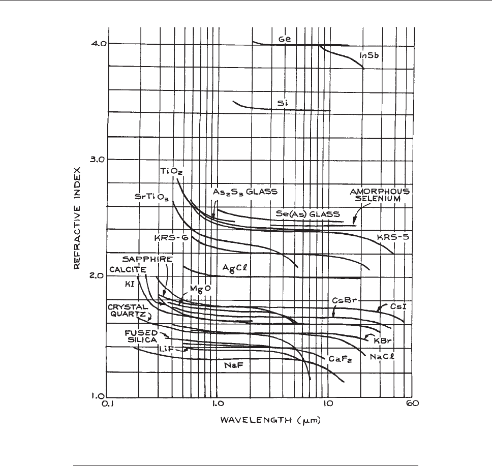
Ultraviolet Transmissive Materials. The following
are suitable for use in the UV region.
(i) Lithium fluoride. Lithium fluoride (LiF, Figure 4.92)
ha
s useful transmittance further into the vacuum ultraviolet
than any other common crystal. The transmission of vac-
uum-ultraviolet quality crystals is more than 50% at 121.6
nm for 2 mm thickness, and thinner crystals have useful
transmission down to 104 nm. The short-wavelength trans-
mission of the material deteriorates on exposure to atmos-
pheric moisture or high-energy radiation. Moisture does not
affect the infrared transmission, which extends to 7 lm.
Several grades of LiF are available. Vacuum-ultraviolet-
grade material is soft, but visible-grade material is hard.
Figure 4.91 The refractive indices of various optical materials. [Adapted, with permission,
from W. C. Wolfe and S. S. Ballard, Optical Materials, Films and Filters for Infrared
Instrumentation, Proceedings of the IRE, 47, 1540-1546, 1959. Ó 1959 IRE (now IEEE).]
OPTICAL MATERIALS 237

LiF can be used as a vacuum-tight window material by
sealing with either silver chloride or a suitable epoxy.
(ii) Magnesium fluoride. Vacuum-ultraviolet-grade mag-
nesium fluoride (MgF
2
, Figure 4.92) transmits farther into
the ultraviolet than any common material except LiF. The
transmission at 121.6 nm is 35% or more for a 2 mm thick-
ness. MgF
2
is recommended for use as an ultraviolet-trans-
missiv e component in space work, as it is only slightly affected
by ionizing radiation. MgF
2
is birefringent and is used for
making polarizing components in the ultraviolet. Irtran 1 is
a polycrystalline form of magnesium fluoride manufactured
by Kodak, which is not suitable for ultra violet or visible appli-
cations. Its useful transmission extends from 500 nm to 9 lm.
(iii) Calcium fluoride. Calcium fluoride (CaF
2
, Figure
4.92) is an excellent, hard material that can be used
for
optical components from 125 nm to beyond 10 lm.
Vacuum-ultraviolet-grade material transmits more than
50% at 125.7 nm for a 2 mm path length. Calcium fluoride
is not significantly affected by atmospheric moisture at
ambient temperature. Calcium fluoride lenses are available
from Argus, Janos Technology, Linos Photonics, Meller
Optics, Melles Griot, Newport, Optovac, Newport/Oriel
and Precision Optical. Irtran 3 is a polycrystalline form
of CaF
2
, which is not suitable for ultraviolet or visible
applications, but transmits in the infrared to 11.5 lm.
(iv) Barium fluoride. Although barium fluoride (BaF
2
,
Figure 4.93) is slightly more water soluble than calcium or
magnesium
fluoride, it is more resistant than either of these
to ionizing radiation. It is a good general-purpose optical
material from ultraviolet to infrared. It has excellent trans-
mission to beyond 10 lm, and windows that are not too
thick (< 2 mm) can be used in CO
2
laser applications,
except at very high energy densities. Barium fluoride
lenses are available from Infrared Optical Products and
International Scientific Products.
(v) Synthetic sapphire. Synthetic sapphire (corundum,
Al
2
O
3
; Figure 4.93) is probably the finest optical material
av ailable in applications from 300 nm to 4 lm. It is v ery hard,
strong, and resistant to moisture and chemical attack (e ven HF
below 300 °C). The useful transmissive range extends from
150nmto6lm, the transmission of a 1 mm thickness being
21% and 34%, respectiv ely, at these two wavelengths. Sap-
phire optical components are available from many suppliers.
31
Sapphire is also resistant to ionizing radiation, has high
thermal conductivity, and can be very accurately fabricated
in a variety of forms. It has low dispersion, however, and is
not very useful as a prism material. Chromium-doped
Al
2
O
3
(ruby) is used in laser applications.
(vi) Fused silica. Fused silica (SiO
2
, Figure 4.94)isthe
amorphous form of crystalline quartz. It is almost as good
Figure 4.92 Transmission curves of lithium fluoride, magnesium fluoride, and calcium
fluoride windows of specified thicknesses.
238 OPTICAL SYSTEMS
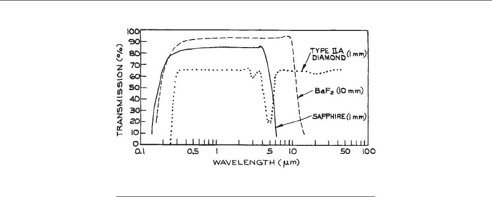
an optical material as sapphire and is much cheaper . Its useful
transmission range extends from about 170 nm to about 4.5
lm. Special ultraviolet-transmitting grades are manufactured
(such as Spectrosil and Suprasil), as well as infrared grades
(such as Infrasil) from which undesirable absorption features
at 1.38, 2.22, and 2.72 lm, due to residual OH radicals, have
been removed. Fused silica has a very low coefficient of
thermal expansion, 5 3 10
–7
/K in the temperature range from
20 to 900 °C, and is very useful as a spacer material in
applications such as Fabry–Perot etalons and laser cavities.
Fused-silica optical components such as windows, lenses,
prisms, and etalons are readily available. Crystalline quartz
is birefringent and is widely used in the manufacture of polar-
izing optics, particularly quarter-wa ve and half-wave plates.
Very pure fused silica is also the material of which most
optical fibers are made. In fiber optic applications the index
gradient inside the fiber is generally produced by germania
(GeO
2
) doping. The pure silica used in optical fibers is most
transparent in the infrared, generally near 1.55 lm.
(vii) Diamond. W indo ws made of type-IIA diamond (Fig-
ure
4.93) have a transmittance that extends from 230 nm to
be
yond 200 lm, although there is some absorption between
2.5 and 6.0 lm. The high refractiv e index of diamond, n ¼
2.4, over a very wide band, leads to a reflection loss of about
34% for two surfaces. Diamond windows are extremely
expensi ve, ($10,000–20,000 for a 1 cm diameter , 1 mm thick
window); howe v er, some properties of diamond are unique:
its thermal conductiv ity is six times that of pure copper at 20
°C, and it is the hardest material known, very resistant to
chemical attack, with a low thermal-expansion coefficient
and high resistance to radiation damage.
Visible- and Near-Infrared-Transmissive
Materials.
The materials so far considered as
ultraviolet-transmitting are also excellent for use in the
visible and near infrared. There are, however, several
materials that transmit well in the visible and near
infrared, but are not suitable for ultraviolet use.
(i) Glasses. There is an extremely large number of types
of glass used in the manufacture of optical components.
They are available from many manufacturers, such as
Chance, Corning, Hoya, Ohara, and Schott.
Two old classifications of glass into cr own and flint glasses
can be related to the glass chart. Cro wn glasses are glasses
with a V value greater than 55 if n
d
<1.6andV >50ifn
d
>
71.6. The flint glasses have V v alues belo w these limits. The
rare earth glasses contain rare earths instead of SiO
2
,whichis
the primary constituent of crown and flint glasses. Glasses
containing lanthanum contain the symbol La.
A few common glasses are widely used in the manufac-
ture of lenses, windows, prisms, and other components.
These include the borosilicate glasses Pyrex, BK7/A, and
crown (BSC), as well as Vycor, which is 96% fused quartz.
Transmission curves for Pyrex No. 7740 and Vycor No.
Figure 4.93 Transmission curves of sapphire, barium fluoride, and
type IIA diamond windows of specified thicknesses.
OPTICAL MATERIALS 239
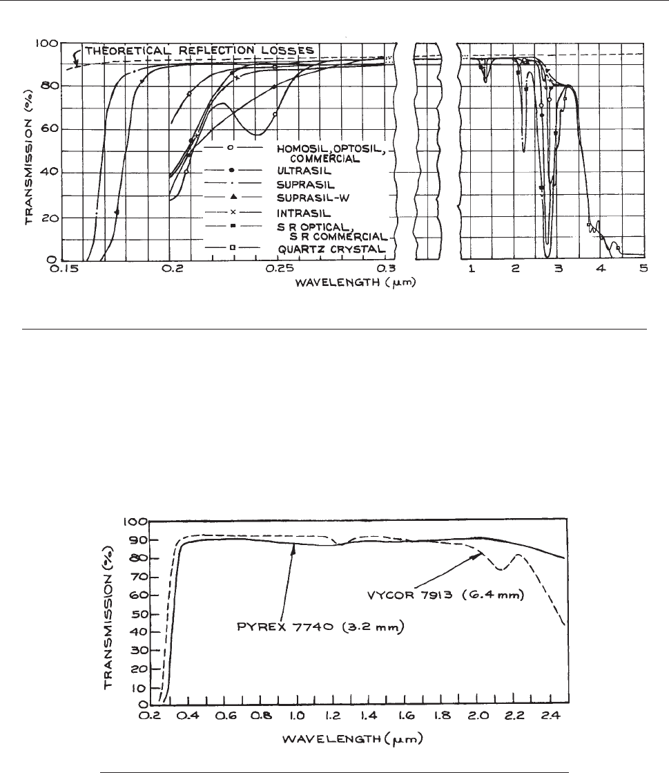
7913 are shown in Figure 4.95. These glasses are not very
useful above 2.5 lm, their transmission at 2.7 lmisdown
to 20% for a 10 mm thickness. In the spectral region
between 350 nm and 2.5 lm, however, they are excellent
transmissive materials. They are inexpensive, hard, and
chemically resistant, and can be fabricated and polished
to high precision. Special glasses for use further into the
infrared are available from Hoya and Corning. In window
applications these glasses do not appear to offer any par-
ticular advantages over more desirable materials such as
infrared-grade fused silica or sapphire; however, in speci-
alized applications, such as infrared lens design, their
higher refractive indices are useful.
For special applications, man y colored filter glasses can be
obtained. Glasses that transmit visible but not infrared, or vice
versa, or that transmit some near ultraviolet, but no visible,
Figure 4.95 Transmission curves for Pyrex 7740 and Vycor 7913.
Figure 4.94 Transmission characteristics of various grades of fused silica; all measurements made on 10 mm thick
materials. (Courtesy of Heraeus-Amersiol, Inc.)
240 OPTICAL SYSTEMS
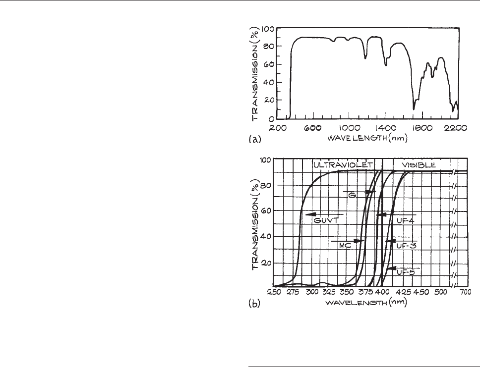
and many other combinations are av ailable. The reader should
consult the catalogs published by the various manufacturers
and suppliers such as Chance-Pilkington, Corning, CVI,
Hoya, Kopp Glass, Melles-Griot (now CVI-Melles-Griot),
NPraezisions Glas & Optik, Schott, and Rolyn.
Special glasses whose expansion coefficients match
selected metals can be made because the composition of
glass is continuously variable,. These glasses are useful for
sealing to the corresponding metals in order to make win-
dows on vacuum chambers. Corning glass No. 7056 is often
used in this way, as it can be sealed to the alloy Kovar.
Vacuum-chamber windows of quartz or sapphire are also
available,
54
but their construction is complex, and conse-
quently they are costly. Various grades of flint glass are
available that have high refractive indices and are therefore
useful for prisms. For a tabulation of the types available the
reader is referred to Kaye and Laby.
7
The refractive indices
available range up to 1.93 for Chance-Pilkington Double
Extra Dense Flint glass No. 927210, but this and other high-
refractive-index glasses suffer long-term damage such as
darkening when exposed to the atmosphere.
(ii) Plastics. In certain noncritical applications, such as
observation windows, transparent plastics such as polyme-
thylmethacrylate (Acrylic, Plexiglas, Lucite, Perspex) or
polychlorotrifluoroethylene (Kel-F) are cheap and satisfac-
tory. They cannot be easily obtained in high optical quality
(with very good surface flatness, for example) and are
easily scratched. The useful transmission range of Acrylic
windows 1 cm thick runs from about 340 nm to 1.6 lm.
A transmission-versus-wavelength curve for this material
is shown in Figure 4.96. One important application of
Acrylic
is in the manufacture of Fresnel lenses (see Section
4.3.3). Kel-F (polychlorotrifluoroethylene) is useful up to
about
3.8 lm, although it shows some decrease in trans-
mission near 3 lm. It is similar to polytetrafluoroethylene
(Teflon) and is very resistant to a wide range of chemicals –
even gaseous fluorine.
(iii) Arsenic trisulfide. Arsenic trisulfide (As
2
S
3
, Figure
4.97) is a red glass that transmits well from 800 nm to 10
lm.
Its usefulness stems from its relatively low price, ease
of fabrication, nontoxicity, and resistance to moisture.
Although primarily an infrared-transmissive material, it is
also transmissive in the red, which facilitates the alignment
of optical systems containing it. As
2
S
3
is relatively soft and
will cold-flow over a long period of time. A wide range of
As
2
S
3
lenses are available from Amorphous Materials,
OFR (Thorlabs), Recon Optical, and REFLEX Analytical.
Middle- and Far-Infrared-Transmissive Materials.
The following are useful well into the IR region.
(i) Sodium chloride. Sodium chloride (NaCl, Figure 4.98)
is
one of the most widely used materials for infrared-trans-
missive windows. Although it is soft and hygroscopic, it
can be repolished by simple techniques and maintained
exposed to the atmosphere for long periods without damage
simply by maintaining its temperature higher than ambient.
Figure 4.96 (a) Transmission curve for 3.175 mm thick
acrylic. (Courtesy of Melles Griot, Inc.); (b) Transmission
curve of various grades of acrylic available from Altumax
International.
OPTICAL MATERIALS 241
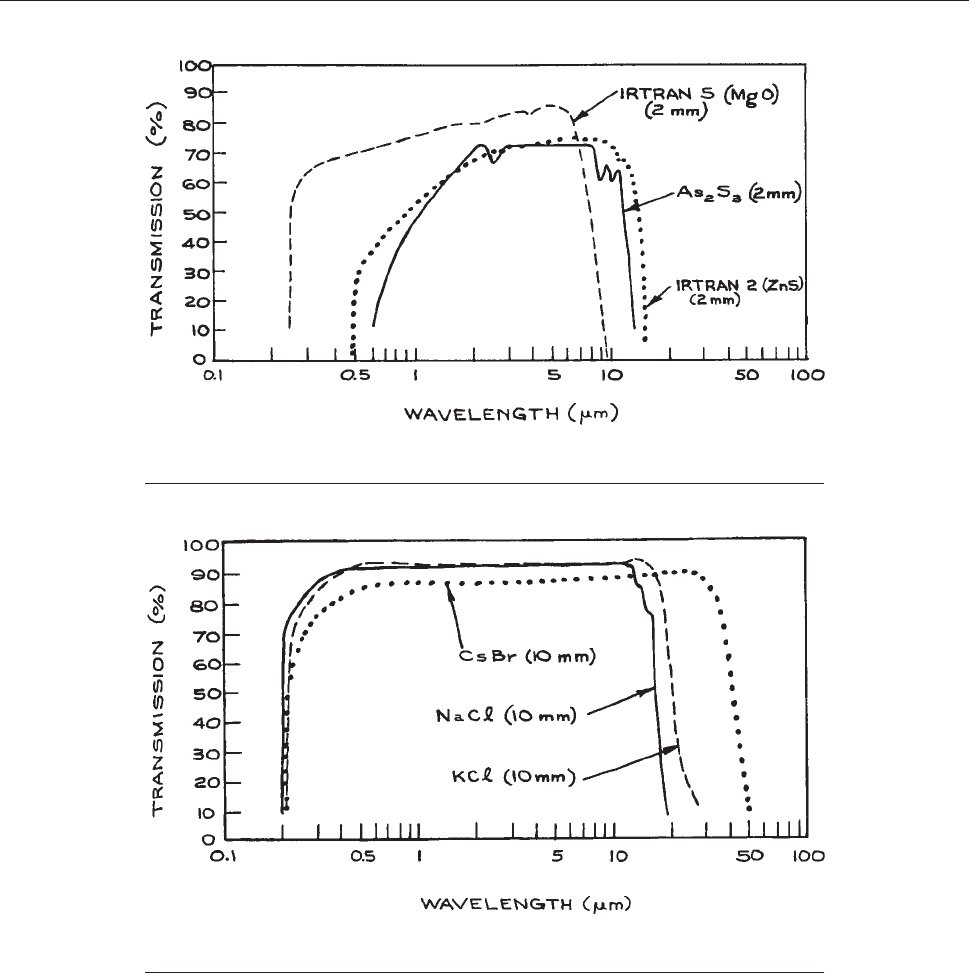
Two simple ways of doing this are to mount a small tung-
sten-filament bulb near the window, or to run a heated wire
around the periphery of small windows. High-precision
sodium chloride windows are in widespread use as Brew-
ster windows in high-energy, pulsed CO
2
laser systems.
(ii) Potassium chloride. Potassium chloride (KCI, Figure
4.98) is very similar to sodium chloride. It is also an excel-
lent
material for use as a Brewster window in pulsed CO
2
lasers, as its transmission at 10.6 lm is slightly greater than
that of sodium chloride.
Figure 4.97 Transmission curves for Irtran 2 (ZnS), Irtran 5 (MgO), and As
2
S
3
windows of
specified thicknesses.
Figure 4.98 Transmission curves for cesium bromide, potassium chloride, and sodium
chloride windows of specified thickness.
242 OPTICAL SYSTEMS
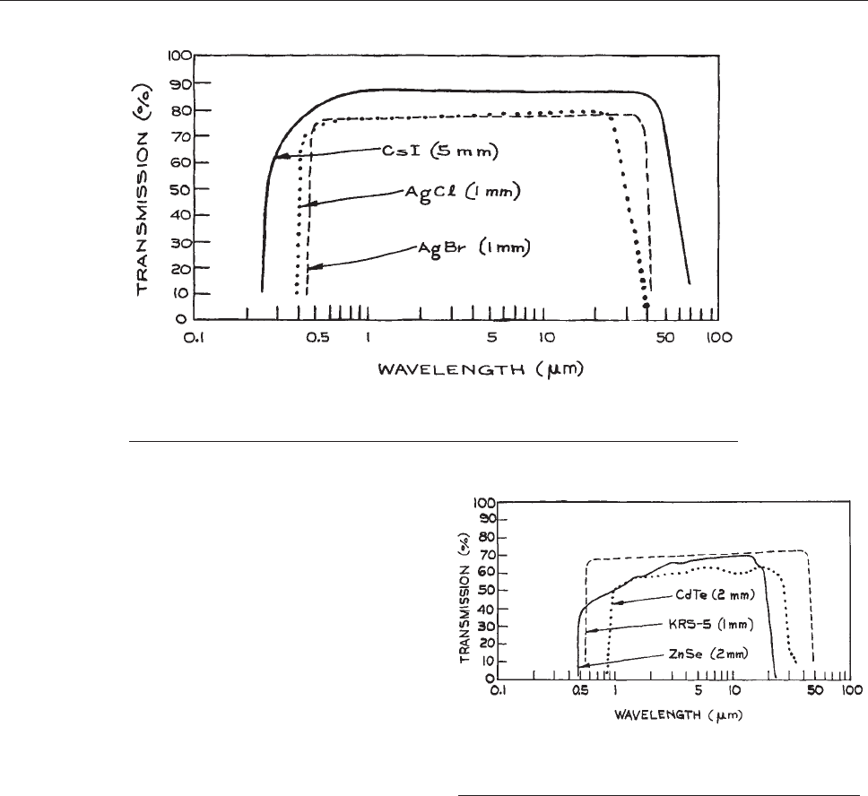
(iii) Cesium bromide. Cesium bromide (CsBr, Figure
4.98) is soft and extremely soluble in water, but has useful
transmission
to beyond 40 lm. It will suffer surface dam-
age if the relative humidity exceeds 35%.
(iv) Cesium iodide. Cesium iodide (CsI, Figure 4.99)is
used
for both infrared prisms and windows; it is similar to
CsBr, but its useful transmission extends beyond 60 lm.
(v) Thallium bromoiodide (KRS-5). Thallium bromoio-
dide (Figure 4.100), widely known as KRS-5, is an impor-
tant
material because of its wide transmission range in the
infrared – from 600 nm to beyond 40 lm for a 5-mm
thickness – and its low solubility in water. KRS-5 will
survive atmospheric exposure for long periods of time
and can even be used in liquid cells in direct contact with
aqueous solutions. Its refractive index is high: reflection
losses at 30 lm are 30% and it has a tendency to cold-flow.
KRS-5 lenses are available from Almaz Optics, Infrared
Optical Products, ISP Optics, and Janos Technology.
(vi) Zinc selenide. Chemical-vapor-deposited zinc sele-
nide (ZnSe, Figure 4.100) is used widely in infrared-
laser
applications. It is transmissive from 500 nm to 22
lm. Zinc selenide is hard enough that it can be cleaned
easily. It is resistant to atmospheric moisture and can be
fabricated into precision windows and lenses. Its trans-
missive qualities in the visible (it is orange-yellow in
color) makes the alignment of infrare d systems using
it much more convenient than in systems using germa-
nium, silicon, or g allium arsenide. Irtran 4 is a polycrys-
talline form of zinc selenide originally developed by
Figure 4.99 Transmission curves for cesium iodide, silver bromide, and silver chloride
windows of specified thicknesses.
Figure 4.100 Transmission curves for zinc selenide,
cadmium telluride, and KRS-5 windows of specified
thicknesses.
OPTICAL MATERIALS 243
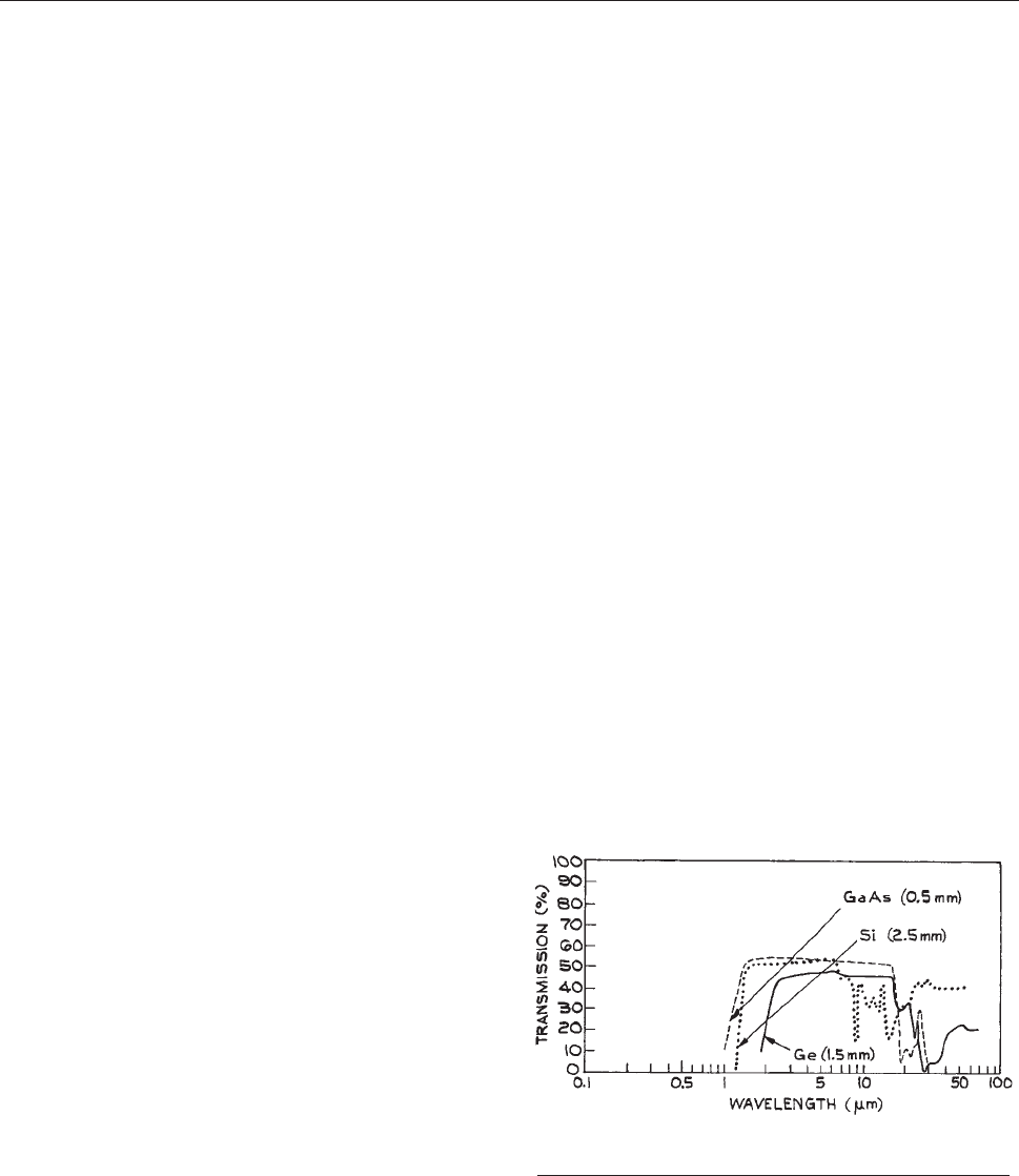
Kodak, which is available from Harrick Scientific and
Perkin Elmer.
(vii) Plastic films. Several polymer materials are sold
commercially in film form, including polyethylene (Poly-
thene, Polyphane, Poly-Fresh, Dinethene, etc.), polyviny-
lidene chloride copolymer (Saran Wrap), polythylene
terephthalate (Mylar, Melinex, Scotchpar), and poly-
carbonate (Lexan). These plastic materials can be used to
wrap hygroscopic crystalline optical components to pro-
tect them from atmospheric moisture. If the film is wrap-
ped tightly, it will not substantially affect the optical
quality of the wrapped components in the infrared. Care
should be taken to use a polymer film that transmits the
wavelength for which the protected component is to be
used. For example, several commercial plastic food wraps
can be used to wrap NaCI or KCI windows for use in CO
2
-
laser applications. Not all will prove satisfactory, however,
and a particular plastic film should be tested for transmis-
sion before use. A note of caution: plastic films contain
plasticizers, the vapor from which may be a problem.
(viii) Plastics and other materials for far-infrared use.
Plastics are widely used for windows, beamsplitters, and
light guides in the far-infrared. A Mylar film is widely used
as the beam-splitting element in far-infrared Michelson
interferometers, and polyethylene, polystyrene, nylon,
and Teflon are used as windows in far-infrared spectrom-
eters and lasers. Black polyethylene excludes visible and
near-infrared radiation, but transmits far-infrared. Lenses
and stacked-sheet polarizers for far-infrared use can be
made from polyethylene. Several crystalline and semicon-
ducting materials, although they absorb in the middle infra-
red, begin to transmit again in the far infrared. A 1 mm
thick quartz window has 70% transmission at 100 lm and
more than 90% transmission from 300 to 1000 lm. The
alkali and alkaline-earth halides such as NaF, LiF, KBr,
KCI, NaCl, CaF
2
, SrF
2
, and BaF
2
show increasing trans-
mission for wavelengths above a critical value that varies
from one crystal to another but is in the 200–400 lm range.
Further details of the specialized area of far-infrared mate-
rials and instrumentation are available in the literature.
55–57
Semiconductor Materials. Several of the most
valuable infrared optical materials are semiconductors.
In very pure form these materials should be transmissive
to all infrared radiation with wavelengths longer than
that corresponding to the band gap. In practice the
long-wavelength transmission will be governed by the
presence of impurities – a fact that is put to good use in
the construction of infrared detectors. Semiconductors
make very convenient ‘‘cold mirrors,’’ as they reflect
visible radiation quite well but do not transmit it.
(i) Silicon. Silicon (Si, Figure 4.101) is a hard, chemically
resistant
material that transmits wavelengths beyond about
1.1 lm. It does, however, show some absorption near 9 lm,
so it is not suitable for CO
2
-laser windows. It has a high
refractive index (the reflection loss for two surfaces is 46%
at 10 lm), but can be antireflection-coated. Because of its
high refractive index it should always be highly polished to
reduce surface scattering. Silicon has a high thermal con-
ductivity and a low thermal expansion coefficient, and it is
resistant to mechanical and thermal shock. Silicon mirrors
can therefore handle substantial infrared-laser power den-
sities. Silicon lenses are available from II-VI Infrared, ISP
Optics, Lambda Research Optics, Laser Research Optics,
Meller Optics, and V.A. Optical.
(ii) Germanium. Germanium (Ge, Figure 4.101) trans-
mits
beyond about 1.85 lm. Very pure samples can be
transparent into the microwave region. It is somewhat brit-
tle, but is still one of the most widely used window and lens
materials in infrared-laser applications. It is chemically
inert and can be fabricated to high precision. Germanium
Figure 4.101 Transmission curves for the semiconductor
materials germanium, gallium arsenide, and silicon.
244 OPTICAL SYSTEMS

has good thermal conductivity and a low coefficient of
thermal expansion; it can be soldered to metal. In use, its
temperature should be kept below 40 °C, as it exhibits
thermal runaway – its absorption increases with increasing
temperature. A wide range of germanium lenses are avail-
able from Lambda Research Optical, Laser Research
Optics, Meller Optics, Umicore, and V.A. Optical.
(iii) Gallium arsenide. Gallium arsenide (GaAs, Figure
4.101) transmits from 1 to 15 lm.
It is a better, although
more expensive, material than germanium, particularly in
CO- and CO
2
-laser applications. It is hard and chemically
inert, and maintains a very good surface finish. It can han-
dle large infrared power densities because it does not
exhibit thermal runaway until it reaches 250 °C. It is also
used for manufacturing infrared-laser electro-optic modu-
lators. Gallium arsenide lenses are available from Infrared
Optical Products ISP Optics, Lambda Research Optics,
and REFLEX Analytical.
(iv) Cadmium telluride. Cadmium telluride (CdTe, Fig-
ure
4.100) is another excellent material for use between 1
and
15 lm. It is quite hard, chemically inert, and takes a
good surface finish. It is also used for manufacturing infra-
red-laser electro-optic modulators. Irtran 6 is a polycrystal-
line form of cadmium telluride available from Kodak; it
transmits to 31 lm. Cadmium telluride lenses are available
from ISP Optics and REFLEX Analytical.
(v) Tellurium. Tellurium is a soft material that is trans-
parent from 3.3 lm to beyond 11 lm. It is not affected by
water. Its properties are highly anisotropic; it can be used
for second harmonic generation with CO
2
-laser radiation.
Tellurium should not be handled, as it is toxic and can be
absorbed through the skin.
4.4.2 Materials for Mirrors
and Diffraction Gratings
Metal Mirrors. The best mirrors for general broad-
band use have pure metallic layers, vacuum-deposited or
electrolytically deposited on glass, fused-silica, or metal
substrates. The best metals for use in such reflective coat-
ings are aluminum, silver, gold, and rhodium. Solid metal
mirrors with highly polished surfaces made of metals such
as stainless steel, copper, zirconium-copper, and molybde-
num are also excellent, particularly in the infrared. The
reflectance of a good evaporated metal coating exceeds
that of the bulk metal. Flat solid-metal mirrors can be made
fairly cheaply by machining the mirror blank, surface-
grinding it, and finally polishing the surface. If precision
polishing facilities are not available, there are numerous
optical component suppliers who will undertake the pol-
ishing of such surface-ground blanks to flatnesses as good
as k/10 in the visible. Finished flat and spherical solid-
metal mirrors are available from II-VI Infrared, Opti-
Forms, Space Optics Research Labs (SORL), and Spawr.
Solid-metal mirrors are most valuable for handling high-
power infrared laser beams when metal-coated mirrors
cannot withstand the power dissipation in the slightly
absorbing mirror surface. Water-cooled copper mirrors
for handling very intense infrared laser beams are available
from Spawr and Umicore Laser Optics Ltd.
The spectral reflectanc es in normal inc idence of sev-
eral common metal coatings are compared in Figure
4.1
02. Several points are worthy of note. Gold and copper
are
not good for use as reflectors in the visible region.
Unprotected gold, silver, copper, and aluminum are very
soft. Aluminum rapidly acquires a protective layer of
oxide after deposi tion; this significantly reduces the
reflectance in the vacuum ultraviolet and contributes to
increased scattering througho ut t he spectrum. Alum inum
and gold are frequently supplied commercially with a thin
protective dielectric layer, which increases their resist-
ance to abrasion without significantly a ffecting their
reflectance, and also protects the aluminum from oxida-
tion. The protective layer is usually a k/2 layer (at 550
nm) of SiO for aluminum mirrors used in the visible
region of the spectrum. Aluminum coated with a thin
layerofMgF
2
canbeusedasareflectorinthevacuum
ultraviolet, although the reflectance is substantially
reduced below about 100 nm, as shown in Figure 4.103.
Man
y optical instruments operating in the vacuum ultra-
violet, including some spectrog raph s, have at leas t one
reflective component. Above 100 nm, coated aluminum is
almost always used for this reflector. Below 100 nm,
platinum and indium have superior reflectance to alumi-
num. At very short wavelengths, below about 40 nm, the
reflectance of platinum in normal incidence is down to
OPTICAL MATERIALS 245
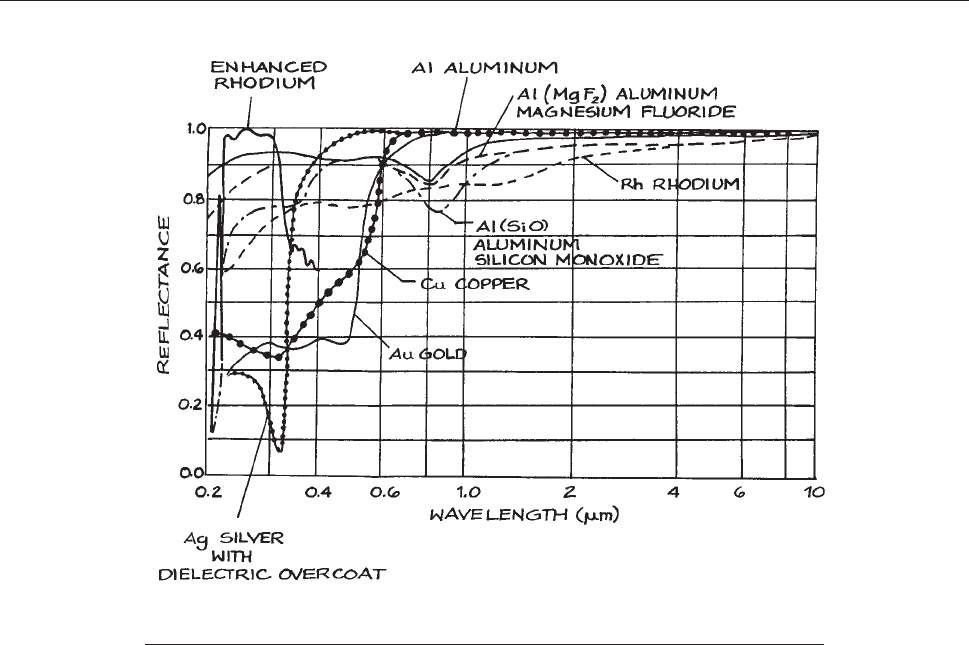
only 10%, as shown in Figure 4.10 3. Therefore, reflective
components in this wavelength region are generally used
at grazing incidence, as the reflectance under these c on-
ditions can remain high. For example, at 0.832 nm the
reflectance of an a lum inum film at a grazing angle of 0.5°
is above 90%.
Freshly evaporated silver has the highest reflectance of
any metal in the visible; however, it tarnishes so rapidly
that it is rarely used except on internal reflection surfaces.
In this case the external surface is protected with a layer of
Inconel or copper and a coat of paint.
Multilayer Dielectric Coatings. Extremely high-
reflectance mirrors (up to 99.99%) can be made by using
multilayer dielectric films involving alternate high- and
low-refractive-index layers, ranging around k/4 thick,
deposited on glass, metal, or semiconductor substrates.
The layers are made from materials that are transparent
in the wavelength region where high reflectance is
required. Both narrow-band and broad-band reflective-
coated mirrors are available commercially. Figure
4.34(a) shows an example of each. Multilayer or single-
layer
dielectric-coated mirrors having almost any desired
reflectance at wavelengths from 150 nm to 20 lm are also
commercially available.
31
Substrates for Mirrors. The main factors influencing
the choice of substrate for a mirror are: (1) the dimensional
stability required; (2) thermal dissipation; (3) mechanical
considerations such as size and weight; and (4) cost. Glass
is an excellent substrate for most totally reflective mirror
applications throughout the spectrum, except where high
thermal dissipation is necessary. Glass is inexpensive and
strong, and takes a surface finish as good as k/200 in the
Figure 4.102 Reflectance of freshly deposited films of aluminum, copper, gold, rhodium,
and coated silver, aluminum and rhodium as a function of wavelength from 0.2 to 10 lm.
246 OPTICAL SYSTEMS
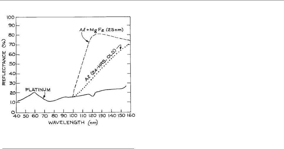
visible. Fused silica and certain ceramic materials such as
Zerodur (available from Schott Glass) are superior, but
more expensive, alternatives to glass when greater
dimensional stability and a lower coefficient of thermal
expansion (CTE) are required. Fused silica has the
lowest CTE, ~5 3 10
–7
/K of any readily available
material. The ceramic Zerodur has a CTE that can be 10
times smaller. The alloy Superinvar has a CTE similar to
quartz, but generally over a restricted temperature range.
Machining or poli shing of low CTE materials can produce
stresses in them and increase their expansion coefficients.
Metal mirrors are frequently used when a very high light
flux must be reflected, but even the small absorpti on loss in
the reflecting surface necessitates cooling of the substrate.
Metals are, however, not so dimensionally stable as glasses
or ceramics, and their use as mirrors should be avoided in
precision applications, particularly in the visible or
ultraviolet.
Partially reflecting, partially transmitting mirrors are
used in many optical systems, such as interferometers
and lasers. In this application the substrate for the mirror
has to transmit in the spectral region being handled. The
substrate material should possess the usually desirable
properties of hardness and dimensional stability, plus the
ability to be coated. For example, germanium, silicon, and
gallium arsenide are frequently used as partially trans-
mitting mirror substrates in the near infrared. Only the
least expensive partially reflecting mirrors use thin metal
coatings. Such coatings are absorbing, and multilayer,
dielectric-coated reflecti v e surfaces are much to be preferred.
There are numerous suppliers of totally and partially
reflecting mirrors.
31
The experimentalist need only deter-
mine the requirements and specify the mirror appropri-
ately.
Mirrors that reflect visible radiation and transmit infra-
red (cold mirrors) or transmit visible radiation and reflect
infrared (hot mirrors) are available as standard items from
several suppliers.
31
Diffraction Gratings. Diffraction gratings are generally
ruledonglass,whichmaythenbecoatedwithaluminum
or gold for visible or infrared reflective use, respectively.
Many commercial gratings are replicas made from a ruled
master, although high-quality holographic gratings are
available from several suppliers.
31
For high-power
infrared-laser applications, gold-coated replica gratings
are unsatisfactory and master gratings ruled on copper
should be used. Such gratings are available from Diffraction
Products, Jobin-Yvon, and Richardson Grating Laboratory
(through Newpo rt).
4.5 OPTICAL SOURCES
Optical sources f all into two categories: incoh erent sour-
ces such as me rcur y or xenon arc, tungsten filament, and
sodium lamps; and coherent sources (las ers). There are
many different types of laser, of which some exhibit a
high degree of coherence and others are not significantly
more coherent than a line source, such as a low-pressure
mercury lam p.
Incoherent sources fall into two broad categories: line
sources and cont inuum sources. Line sources emit most
of their radiation at discret e wavelengths, which corre-
spond to strong spectral emission features of the excited
atom or ion that is the emitting species in the source.
Continuum sources emit over some broa d spectral
region, although their radiant intensity varies with wave-
length.
Figure 4.103 Normal-incidence reflectance of platinum,
aluminum with a 25 nm thick overcoat of MgF
2
, and
unprotected aluminum 24 hours after film deposition.
OPTICAL SOURCES 247
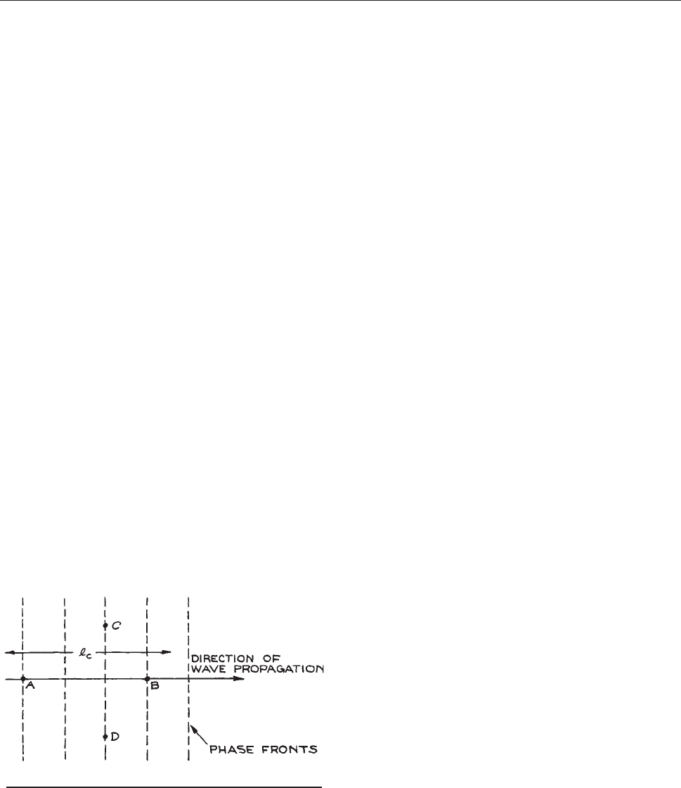
4.5.1 Coherence
There are two basic coherence properties of an optical
source. One is a measure of its relative spectral purity. The
other depends on the degree to which the wavefronts coming
from the source are uni phase or of fixed spatial phase varia-
tion. A wavefront is said to be uniphase if it has the same
phase at all points on the wavefront. The Gaussian TEM
00
mode emitted by many lasers has this property.
The two types of coherence are illustrated by Figure 4.104.If
the
phases of the electromagnetic field at two points, A and B,
longitudin ally separate d in the direction of propagation, have a
fixed relationship, then the wave is said to be temporally coher-
ent for times corresponding to the distance from A to B.The
existence of such a fixed phase relationship could be demon-
strated by combining waves extracted at points separated like
A and B and producing an interference pattern. The Michelson
interferometer (see Section 4.7.6) demonstrates the existence
of
such a fixed phase relationship. The maximum separation
of A and B for which a fix ed phase relationship exists is called
the coher ence length of the source l
c
. The coherence length
of a source is related to its coherence time s
c
by:
l
c
¼ cs
c
ð4:191Þ
Conceptually l
c
is the average length of the uninterrupted
wave trains from the source between random phase inter-
ruptions. Fourier theory demonstrates that the longer in
time a sinusoidal wave train is observed, the narrower is
its frequency spread. Thus the spectral width of a source
can be related to its coherence time by writing:
Dm ’ 1=s
c
ð4:192Þ
The most coherent conventional lamp sources are stabi-
lized low-pressure mercury lamps, which can have s
c
rang-
ing up to about 10 ns. Lasers, however, can have s
c
ranging
up to at least 1 ms.
Spatial coherence is a measure of phase relationships in
the wavefront transverse to the direction of wave propaga-
tion. In Figure 4.104, if a fixed phase relationship exists
be
tween points C and D in the wavefront, the wave is said
to be spatially coherent over this region. The area of coher-
ence is a region of the wavefront within which all points
have fixed phase relationships. Spatial coherence can be
demonstrated by placing pinholes at different locations in
the wavefront and observing interference fringes. Tempo-
rally incoherent sources can exhibit spatial coherence.
Small sources (so-called point sources) fall into this cate-
gory. The light from a star can be spatially coherent.
Extended, temporally incoherent sources have a low
degree of spatial coherence because light coming from
different parts of the source has different phases. Lasers
emitting a TEM
00
(fundamental) mode have very good
spatial coherence over their whole beam diameter.
4.5.2 Radiometry: Units and Definitions
Radiometry deals with the measurement of amounts of
light. In radiometric terms the characteristics of a light
source can be specified in several ways.
Radiant power, W, measured in watts, is the total amount
of energy emitted by a light source per second. The spec-
tral variation of radiant power can be specified in terms of
the radiant power density per unit wavelength interval, W
k
.
Clearly:
W ¼
ð
‘
0
W
k
dk ð4:193Þ
If a light source emits radiation only for some specific
duration – which may be quite short in the case of a flash-
lamp – it is more useful to specify the source in terms of its
radiant energy output, Q
e
, measured in joules. If the source
emits radiation for a time T, we can write:
Q
e
¼
ð
T
0
WðtÞdt ð4:194Þ
Figure 4.104 Temporal and spatial coherence.
248 OPTICAL SYSTEMS
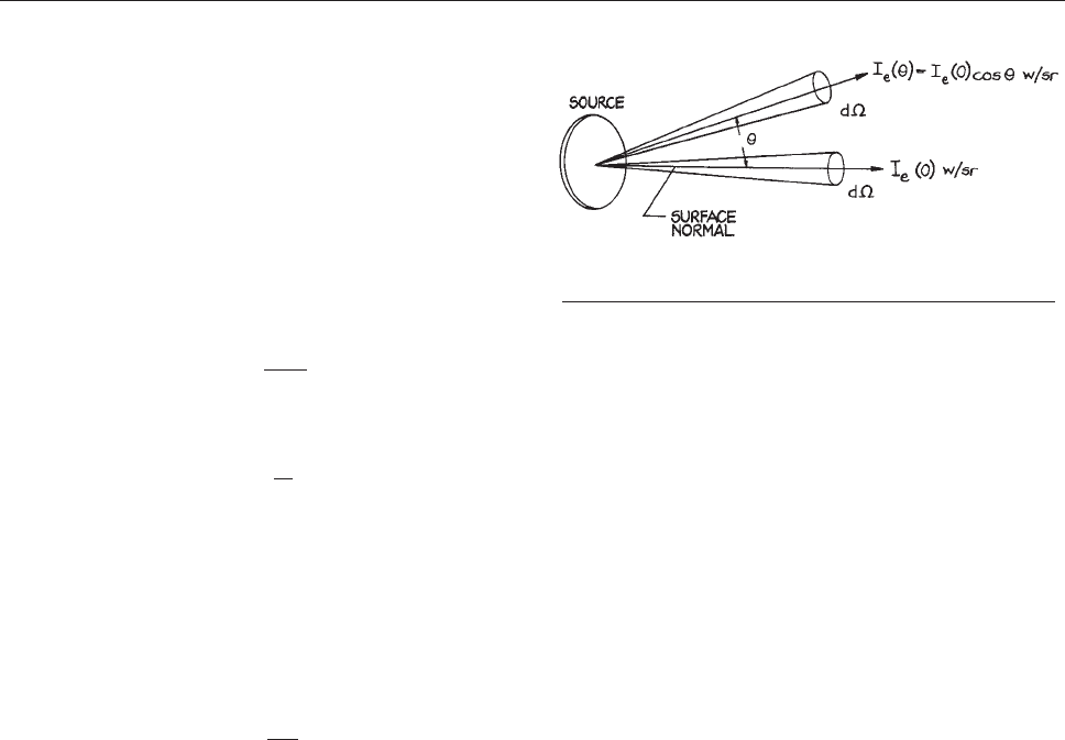
The amount of power emitted by a source in a particular
direction per unit solid angle is called radiant intensity I
e
,
and is measured in watts per steradian. In general:
W ¼ I
e
ðxÞdx ð4:195Þ
where the integral is taken over a closed surface surround-
ing the source. If I
e
is the same in all directions, the source
is said to be an isotropic radiator. At a distance r from such
a source, if r is much greater than the dimensions of the
source, the radiant flux crossing a small area DS is:
/
e
¼
I
e
DS
r
2
ð4:196Þ
The irradiance at this point, measured in W/m
2
, is:
E
e
¼
I
e
r
2
ð4:197Þ
which is equal to the average value of the Poynting vector
measured at the point. The radiant flux emitted per unit
area of a surface (whether this be emitting or merely
reflecting and scattering radiation) is called the radiant
emittance M
e
, and it is measured in W/m
2
. For an extended
source, the radiant flux emitted per unit solid angle per unit
area of the source is called its radiance or brightness L
e
:
L
e
¼
dI
e
dS
n
ð4:198Þ
where the area dS
n
is the projection of the surface element
of the source in the direction being considered. When the
light emitted from a source or scattered from a surface has
a radiance that is independent of viewing angle, the source
or scatterer is called a perfectly diffuse or Lambertian
radiator. Clearly, for such a source, the radiant intensity
at an angle h to the normal to the surface is:
I
e
ðhÞ¼I
e
ð0Þcos h ð4:199Þ
as illustrated in Figure 4.105.
The
total flux emitted per unit area of such a surface is
its radiant emittance, which in this case is:
M
e
¼ pI
e
ð0Þð4:200Þ
Illuminated diffusing surfaces made of finely ground glass
or finely powered magnesium oxide will behave as Lam-
bertian radiators.
For plane waves, since all the energy in the wave is
transported in the same direction, the concepts of
radiant int ensity and emittance are not u seful. It is
customary to specify the radiant flux crossing unit
area normal to the direction of propagation, and call this
the intensity I of the plane wave. Because lasers emit radi-
ation into an extremely small solid angle, they have very
high radiant intensity, and it is once again more usual to
refer simply to the intensity of the laser beam at a point as
the energy flux per second per unit area. The total power
output of a laser is:
W ¼
ð
beam
IdS ð4:201Þ
4.5.3 Photometry
Photometry is the measurement of light that is in, or close
to, the spectral region where the human eye responds. It is
related to radiometry, but its units are weighted by the
response of the human eye. The human eye provides a
nonlinear and wavelength-dependent subjective impres-
sion of radiometric quantities. The response function of
the human eye extends roughly from 360 to 700 nm, with
a peak at 555 nm for the photopic (light-adapted) eye,
where the cones are the dominant receptors. The dark-
adapted human eye exhibits the scotopic response, which
comes from the light- (but not color-) sensitive rods in the
periphery of the retina. The photopic and scotopic
response are shown in Figure 4.106. Measures in photo-
metry
take into account the so-called photopic spectral
luminous efficiency function V(k). Thus, for example, in
Figure 4.105 Radiant intensity characteristics of a
Lambertian radiator.
OPTICAL SOURCES 249
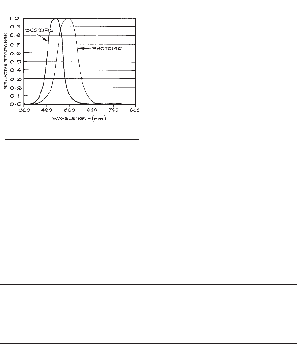
physiological photometry the luminous flux F is related to
radiant flux /
e
(k) by:
F ¼ K
ð
‘
0
VðkÞ/
e
ðkÞdk ð4:202Þ
where K is a constant. When F is measured in lumens and
/
e
(k) in watts, K ¼ 683 lumen W
1
. In practice, the integral
in Equation (4.202) need only be evaluated between
360 nm and 830 nm, as V(k) is zero outside this range.
Other photometric quantities that may be encountered in
specifications of light sources are as follows:
(1) The luminous intensity I
m
measured as candela (Cd),
where:
1 candela ¼ 1 lumen per sr
This is the photometric equivalent of the radiometric
quantity radiant intensity. The formal scientific speci-
fication of the candela is that it is the luminous inten-
sity, in a given direction, of a source that emits
monochromatic radiation of wavelength 550 nm and
that has a radiant intensity in that direction of 1/683
watt per steradian.
(2) The illuminance, E
m
measured in lumen/m
2
[ lux;
lumen/cm
2
[ phot; or lumen/ft
2
[ footcandle.
(3) The luminance or brightness, L
m
measured in candela/m
2
[ nit; candela/cm
2
[ stilb; candela/p ft
2
[ footlambert;
candela/p m
2
[ apostilb; or candela/p cm
2
lambert.
(4) The luminous energy, Q
m
, measured in lumen seconds [
talbot. The correspondences between radiometric and
photometric quantities are summarized in Table 4.6.
For a Lambertian source the luminance is independent
of
the observation direction. Photometric description of the
characteristics of light sources should be avoided in strict
scientific work, but some catalogs of light sources use
photometric units to describe lamp performance. For fur-
ther details of photometry, and other concepts, such as
color in physiological optics, the reader should consult
Levi
24
or Fry.
58
Calibration standards and devices for radiometric and
photometric calibration of light sources are available from
Gamma Scientific, International Light, Optronic Labora-
tories, and UDT Instruments (formerly Graseby).
4.5.4 Line Sources
Line sources are used as wavelength standards for calibrat-
ing spectrometers and interferometers; as sources in
atomic absorption spectrometers; in interferometric
Figure 4.106 The photopic and scotopic spectral
response of the human eye.
Table 4.6 Correspondence between radiometric and photometric quantities
Radiometric Quantity Radiometric Unit Photometric Quantity Photometric Unit
Radiant power watt (W) Power lumen (lm)
Radiant emittance Wm
2
Illuminance lumen m
2
¼lux (lx)
Radiant intensity W/sr Luminous intensity lumen/sr ¼candela (cd)
Radiance (Brightness) Wm
2
sr
1
Luminance (Brightness) lm m
2
sr
1
¼cd m
2
¼nit
Radiant Energy Joule Luminous Energy lm s [ talbot
250 OPTICAL SYSTEMS
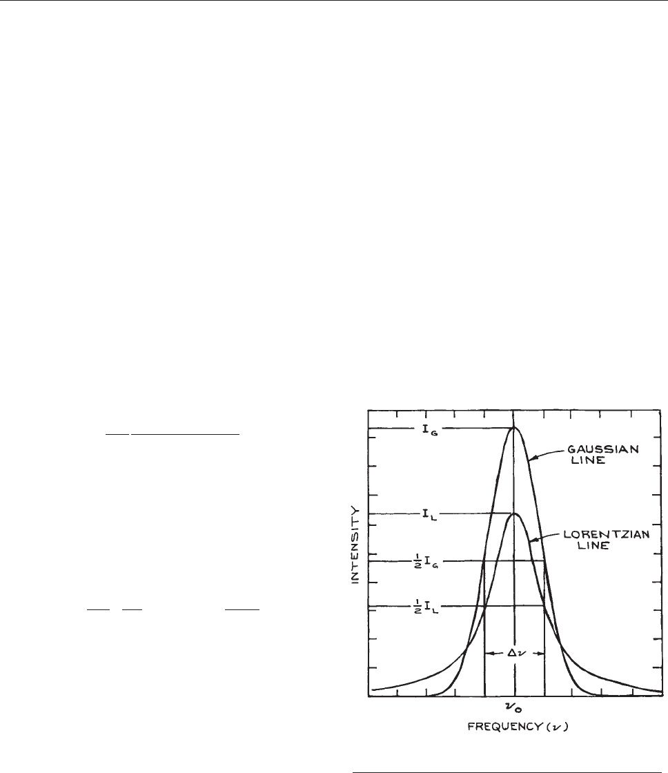
arrangements for testing optical components, such as
Twyman–Green interferometers (Section 4.7.6); in a few
special
cases for optically pumping solid-state and gas
lasers; and for illumination.
The emission lines from a line source are not infinitely
sharp. Their shape is governed by the actual conditions and
physical processes occurring in the source. The variation
of the radiant intensity with frequency across a line whose
center frequency is v
0
is described by its lineshape function
g(v, v
0
), where:
ð
‘
‘
gðv,v
0
Þdv ¼ 1 ð4:203Þ
The extension of the lower limit of this integral to neg-
ative frequencies is done for formal theoretical reasons
connected with Fourier theory and need not cause any
practical problems, since for a sharp line the major con-
tribution to the integral in Equation (4.203) comes from
frequencies
close to the center frequency v
0
. There are
three main types of lineshape function:
59
Lorentzian,
Gaussian, and Voigt.
The Lorentzian lineshape function is:
g
L
ðv,v
0
Þ¼
2
pDv
1
1 þ v v
0
ðÞ=Dv½
2
ð4:204Þ
where Dv is the frequency spacing between the half-inten-
sity points of the line (the full width at half maximum
height, or FWHM). Spectral lines at long wavelengths
(in the middle and far infrared) and lines emitted by heavy
atoms at high pressures and/or low temperatures frequently
show this type of lineshape.
The Gaussian lineshape function is:
g
D
ðv,v
0
Þ¼
2
Dv
D
ln 2
p
1=2
exp 2
v v
0
Dv
D
2
ln 2
()
ð4:205Þ
where Dv
D
is the FWHM. Spectral calibration lamps are
available from Avantes, Cathodeon, Gamma Scientific,
Heraus Nobleight, Newport/Oriel, Ocean Optics, Spectral
Products, and Resonance. Gaussian lineshapes are usually
associated with visible and near-infrared lines emitted by
light atoms in discharge-tube sources at moderate pres-
sures. In this case, the broadening comes from the varying
Doppler shifts of emitting species, whose velocity distri-
bution in the gas is Maxwellian. Emitting ions in real
crystals sometimes have this type of lineshape because
of the random variations of ion environment within a real
crystal produced by dislocations, impurities, and other lat-
tice defects. A Lorentzian and a Gaussian lineshape are
compared in Figure 4.107.
Frequently
, the broadening processes responsible for
Lorentzian and Gaussian broadening are simultaneously
operative, in which case the resultant lineshape is a con-
volution of the two and is called a Voigt profile.
15
The low-pressure mercury lamp is the most commonly
used narrow-line source. These lamps actually operate
with a mercury–argon or mercury–neon mixture. The prin-
cipal lines from a mercury–argon lamp are listed in Table
4.7. Numerous other line sources are also available.
In
particular, hollow-cathode lamps emit the strongest
spectral line of any desired element for use in atomic
absorption spectrometry. Such lamps are available from
Bulbtronics, GBC Scientific Equipment, Hamamatsu,
Figure 4.107 Gaussian and Lorentzian lineshapes of the
same FWHM, Dm.
OPTICAL SOURCES 251

Hellma International, REFLEX Analytical, Semicon Asso-
ciates, and Vitro Technology, Ltd.
4.5.5 Continuum Sources
A continuum source in con junction with a mon ochroma-
tor can be used to obtain radiation whose wavelength
is tunable throughout the emission range of the source.
If the wavelength region transmitted by the monochro-
mator is made very small, not very much energy will
be available in th e wavelength region se lected. E ven
so, continuum sources find extensive use in this way in
absorption and fluorescence spectrometers. Certa in
continuum sources , called b lackbody sources, h ave
very well-characterized radiance as a function of wave-
length and are used for calibrating both the absolute
sensitivity of detecto rs and the absolute radiance of
other sources.
Blackbody Sources. All objects are continuously
emitting and absorbing radiation. The fraction of
incident radiation in a spectral band that is absorbed by
an object is called its absorbtivity. When an object is in
thermal equilibrium with its surroundings, it emits and
absorbs radiation in any spectral interval at equal rates.
An object that absorbs all radiation incident on it is
called a blackbody – its absorbtivity a is equal to unity.
The ability of a body to radiate energy in a particular
spectral band compared to a blackbody is its emissivity.
A blackbody is also the most efficient of all emitters –
its emissivity e is also unity. In general, for any object
emitting and absorbing radiation at wavelength k, e
k
¼ a
k
.
Highly reflecting, opaque objects, such as polished metal
surfaces, do not absorb radiation efficiently; nor, when
heated, do they emit radiation efficiently.
The simplest model of a blackbody source is a heated
hollow object w ith a small hole in it. Any radi ation enter-
ing the hole has minimal chan ce of re-emerging. Conse-
quently, the radiation leaving the hole will be
characteristic of the interi or temperature of the object.
The e nergy density distribution of this blackbody radia-
tion in frequency is:
qðvÞ¼
8phv
3
c
3
1
e
hv=kT
1
ð4:206Þ
where q(v)dv is the energy stored (J/m
3
) in a small fre-
quency band dv at v. The energy density distribution in
wavelength is:
qðkÞ¼
8phc
k
5
1
e
hc=kkT
1
ð4:207Þ
This translates into a spectral emittance (the total power
emitted per unit wavelength interval into a solid angle 2p
by unit area of the blackbody) given by:
M
ek
¼
C
1
k
5
ðe
C
2
=kT
1Þ
ð4:208Þ
where C
1
¼ 2phc
2
, called the first radiation constant, has
the value 3.7418 3 10
–16
Wm
2
/s, and C
2
¼ ch/k, called the
second radiation constant, has the value 1.43877 3
10
–2
mK.
Table 4.7 Characteristic lines from a mercury lamp
Wavelength
a
(lm)
0.253652
0.313156
0.313184
0.365015
0.365483
0.366328
0.404656
0.435835
0.546074
0.576960
0.579066
0.69075
0.70820
0.77292
1.0140
1.1287
3.9425
Note: Extensive listings of calibration lines from other sources
cab be found in C.R. Harrison M.I.T. Wavelength Tables, M.I.T.
Press, Cambridge, Mass, 1969; and in A. R. Striganov and N. S.
Sventitskii, Tables of Spectral Lines of Neutral and Ionized
Atoms, IFT/Plenum Press, New York, 1968.
a
In tacuo.
252 OPTICAL SYSTEMS
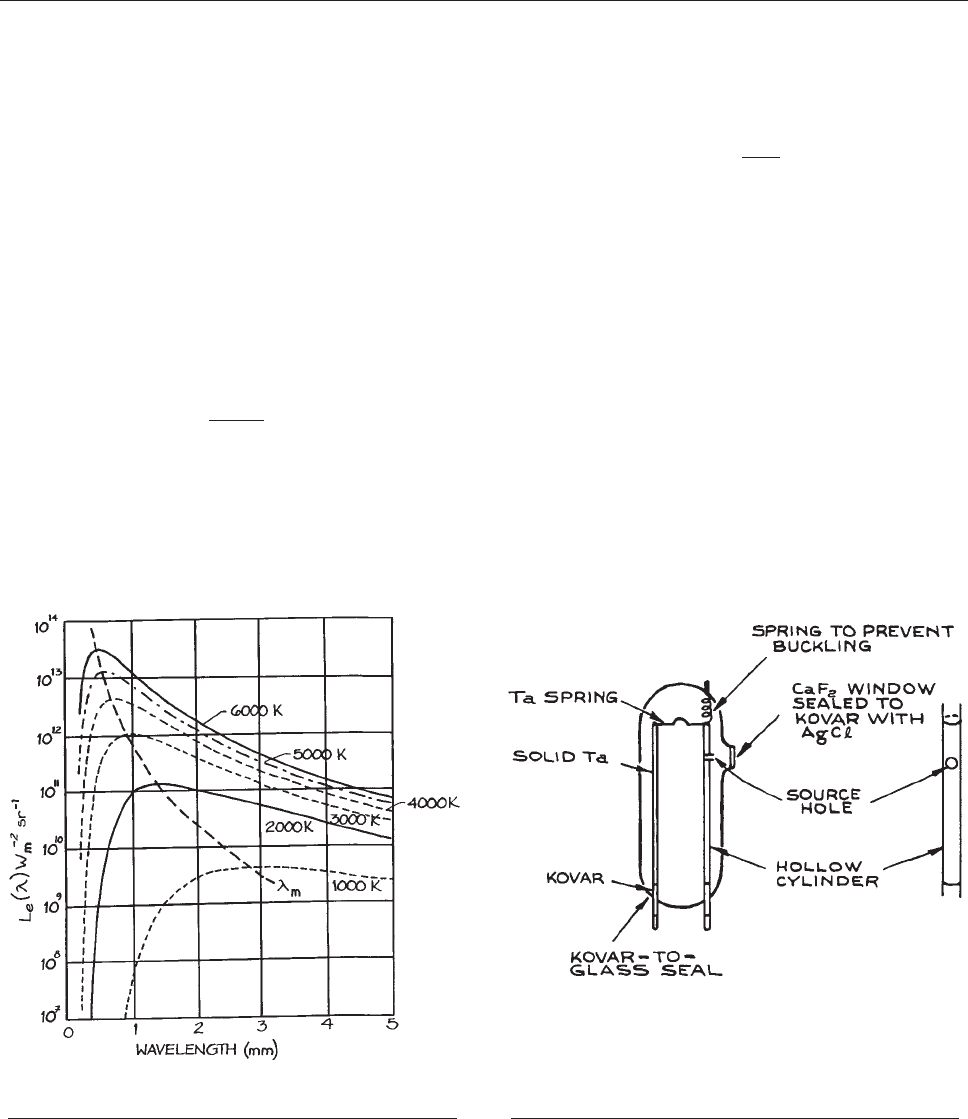
A true blackbody is also a diffuse (Lambertian) radiator.
Its radiance is independent of the viewing angle. For such a
source:
M
ek
¼ pL
ek
ð4:209Þ
The variation of L
ek
with wavelength for various values of
the temperature is shown in Figure 4.108. The wavelength
of
maximum emittance, k
m
at temperature T obeys Wien’s
displacement law:
k
m
T ¼ 2:8978 3 10
3
mK ð4:210Þ
The total radiant emittance of a blackbody at temper-
ature T is:
M
e
¼
ð
‘
0
M
ek
dk ¼
2p
5
k
4
15c
2
h
3
T
4
¼ rT
4
ð4:211Þ
This is a statement of the Stefan–Boltzmann law. The
coefficient r, called the Stefan–Boltzmann constant, has
a value of 5.6705 3 10
–8
Wm
–2
K
–4
. The known param-
eters M
ek
and M
e
of a blackbody allow it to be used as an
absolute calibration source in radiometry. If a detector
responds to photons, the spectral emittance in terms of
photons, N
k
, may be useful:
N
k
¼
M
ek
hc=k
ð4:212Þ
Curves of N
k
are given by Kruse, McGlauchlin, and
McQuistan.
60
A source whose spectral emittance is identical to that of
a blackbody apart from a constant multiplicative factor is
called a graybody. The constant of proportionality, e, is its
emissivity. Several continuum sources, such as tungsten-
filament lamps, carbon arcs, and flashlamps, are approxi-
mately graybody emitters within certain wavelength regions.
Practical Blackbody Sources. The radiant emittance
of a blackbody increases at all wavelengths as the
temperature of the blackbody is raised, so a practical
blackbody should, ideally, be a heated body with a small
emitting aperture that is kept as small as possible. Kruse,
McGlauchlin, and McQuistan
60
describe such a source,
illustrated in Figure 4.109, that can be operated at
Figure 4.108 Spectral radiance L
ek
of a blackbody source
at various temperatures.
Figure 4.109 Construction details of a simple
high-temperature blackbody source. (From P. W. Kruse,
L. D. McGlauchlin, and R. B. McQuistan, Elements of
Infrared Technology: Generation, Transmission, and
Detection, John Wiley & Sons, Inc., New York, 1962;
by permission of John Wiley & Sons, Inc.)
OPTICAL SOURCES 253
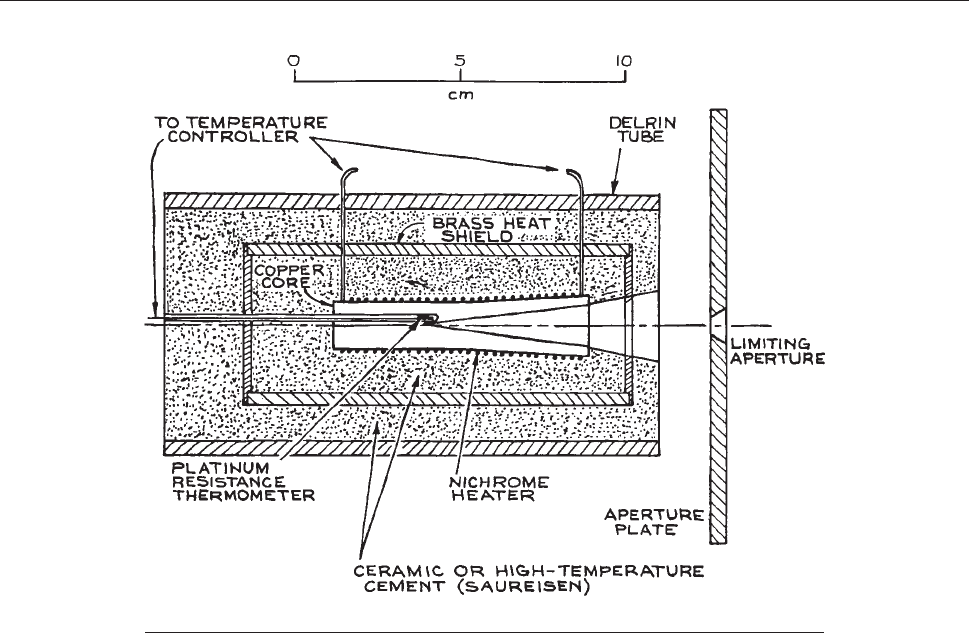
temperatures as high as 3000 K. A 25-lm-thick tungsten
ribbon 2 cm wide is rolled on a 3-mm-diameter copper
mandrel and seamed with a series of overlapping spot
welds. A hole about 0.75 mm in diameter is made in the
foil, and the copper dissolved out with nitric acid under a
fume hood. The resulting cylinder is mounted on 1-mm-
diameter Kovar or tungsten rod feedthroughs in a glass
envelope and heated from a high-current, low-voltage
power supply. The glass envelope should be fitted with a
window that is transmissive to the wavelength region
desired from the source.
Another design of blackbody source is shown in Figure
4.110. This design is based on a heated copper cylinder,
containing
a conical cavity of 15° semivertical angle, that
is allowed to oxidize during operation (so that it becomes
nonreflective and consequently of high emissivity). The
cylinder is heated by an insulated heater wire wrapped
around its circumference. If nichrome wire is used, the
cylinder can be heated to about 1400 K. This assembly
is mounted in a ceramic tube (alumina is quite satisfactory)
or potted in high-temperature ceramic cement. For high-
temperature operation, the whole assembly can be
mounted inside a water-cooled block.
A popular blackbody source uses a ‘‘Globar,’’ a rod of
bonded silicon carbide. In the high-temperature blackbody
source supplied by Newport/Oriel this has been replaced
by pyrolytic graphite. For further details of the advantages
and disadvantages of this and various other blackbody
sources, the reader is referred to Hudson.
61
Blackbody
sources are available commercially from The Eppley Lab-
oratory, HGH Optronics, Infrared Industries, Isotech,
Micron, Omega, and Newport/Oriel.
Tungsten-Filament Lamps. T ungsten-filament lamps
are approximately graybodies in the visible with an
emittance between 0.45 and 0.5. Such lamps are
Figure 4.110 Construction details of an NBS-type blackbody source.
254 OPTICAL SYSTEMS

frequently desc ribed i n terms of their color temperature
T
c
, which is the temperature at which a blackbody would
have a spectral emittance closest in shape to the lamp’s.
The color temperature will depend on the operating
conditions of the lamp.
Tungsten-filament lamps can most conveniently be
operated in the laboratory with a variable transformer.
For best stability and freedom from ripple on their output,
however, they should be operated from a stabilized d.c.
supply. Typical supply requirements range up to a few
hundred volts. Lamps with wattage ratings up to 1 kW
are readily available.
Small tungsten-filament lamps that can be used as point
sources are available from Newport/Oriel. Very-long-life,
constant-efficiency tungsten–halogen lamps are available,
in which the lamp envelope usually contains a small
amount of iodine. In operation, the iodine vaporizes and
recombines with tungsten that has evaporated from the
filament and deposited on the inside of the lamp envelope.
The tungsten iodide thus formed diffuses to the hot fila-
ment, where it decomposes, redepositing tungsten on the
filament. The constant replacement of the filament in this
way allows it to be operated at very high temperature and
radiant emittance. Because the lamp envelope must with-
stand the chemical action of hot iodine vapor and high
temperatures, it is made of quartz. Hence such lamps are
frequently called quartz–iodine lamps. Such lamps can be
quite compact: a 1 kW lamp will have a filament length of
about 1 cm. They are available from Bulb Direct and
Ocean Optics. The National Institute of Standards and
Technology (NIST) standard of spectral irradiance consists
of a quartz–iodine lamp with a coiled-coil tungsten fila-
ment operating at about 3000 K and calibrated from
250 nm to 2.6 lm against a blackbody source. Such cali-
brated lamps are available from EG&G and Newport/
Oriel. Because they are intense sources of radiant energy,
these lamps can also be used for heating. In particular, they
are often placed inside complex vacuum systems to bake
out internal components that are well insulated thermally
from the chamber walls.
Continuous Arc Lamps. High-current electrical
discharges in gases, with currents that typically range
from 1 to 100 A, can be intense sources of continuum or
line emission, and sometimes both at the same time. For
substantial continuum emission the most popular such
lamps are the high-pressure xenon, high-pressure mercury,
and high-pressure mercury–xenon lamps. The arc in these
lamps typically ranges up to about 5 cm long and 6.2 mm in
diameter (for a 10 kW lamp – 100 V, 100 A input). Because
of their small size, arc lamps have much higher spectral
radiance (brightness) than quartz–iodine lamps of
comparable wattage. In the visible region at 500 nm, a
typical xenon arc lamp shows 1.9 times the output of a
quartz–iodine lamp; at 350 nm, 14 times; and at 250 nm,
200 times. In addition, because of their small size, high-
pressure arc lamps work well in the illumination of
monochromator slits in spectroscopic applications. Lower-
wattage arc lamps come close to being point sources and are
ideal for use in projection systems and for obtaining well-
collimated beams.
There are two different kinds of high-pressure arc
lamps: those where the discharge is confined to a narrow
quartz capillary (which must be water-cooled), and those
where the discharge is not confined (which usually
operate with forced-air cooling). The former are available
from Flashlamps (Verre et Quartz), ILC Technology,
Xenon Corp., and Ushio and are used for pumping
CW solid-state lasers. (Krypton arc lamps are better than
xenon arc lamps for pumping Nd
3+
lasers, as their
emission is better matched to the absorption spectrum of
Nd
3+
ions.)
Because high-pressure a rc lamps operate at very
high pressures when hot (up to 200 bar), they must be
housed in a rugged metal enclosure to contain a possible
lamp explosion. The mounting must be such as to
allow s tress-free expansion during warmup. Genera lly
speaking, commercial lamp assemblies should be used.
The power-supply requirements are somewhat unusual.
An initial high-voltage pulse is necessary to strike the
arc, and then a lower voltage, typically in the range 70–
120 V, to establish the arc. When the arc is fully estab-
lished, the operating voltage will drop to perhaps as low
as 10 V. Arcs containing mercury need a further increase
in operating voltage as they warm up and their internal
mercury pressure inc reases. Complete lamp assemblie s
and power supplies are available from several compa-
nies, among them, ILC Tec hnology, Newport/Oriel,
ORC Lighting Products, Perkin Elmer, and Spectral
Energy.
OPTICAL SOURCES 255
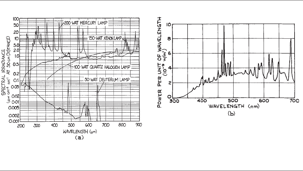
High-pressure arc lamps give substantial continuum
emission with superimposed line structure, as can be seen
in Figure 4.111. These lamps are not efficient sources of
infrared
radiation. They give substantial UV emission,
however, and care should be taken in their use to avoid
eye or skin exposure. Their UV output will also generate
ozone, and provision should be made for venting this
safely from the lamp housing. They are available from
Bulbtronics, Hamamatsu, Laser Drive, Lighting Technol-
ogies International, and Newport/Oriel.
Deuterium lamps are efficient sources of ultraviolet
emission with very little emission at longer wave-
lengths, as shown in Figure 4.111(a). They are available
from
Catheodeon, Hamamatsu, Newport/Oriel, Ocean
Optics, a nd Spectral Energy. Hollow-cathode lamps,
available from Hamamatsu and Hellma, emit stong spec-
tral lines characteristic of the material of which their
cathode is made. They can be used as wavelength cali-
bration sources.
Discharges in high-pressure noble gases can also be
used as intense continuum sources of vacuum-ultraviolet
radiation. This radiation arises from noble-gas excimer
emission, which in the case of helium, for example, arises
from a series of processes that can be represented as:
He þe ! He
,
He
þHe ! He
2
,
He
2
! He þ He þ hv
ð4:213Þ
The spectral regions covered by the excimer continua
are He, 10 5–400 nm; Ar, 107–165 nm; Kr, 124 –185 nm;
and Xe, 147–225 nm. Because there are no tra nsmissive
materials available for wavelengths below about 110
nm, sources below this wavelength are used without
windows. Radiation leaves the lamp through a small slit,
or through a multicapillary array. The latter is a close-
packed array of m any capillary tubes, which presents
considerable resistance to the passage of gas, but is
highly transparent to light. Multicapillary arrays can
be obtained from Burle Electro-Optics. To maintain
the lamp pressure, gas is continuously admitted. Gas
that passes from the lamp into the rest of the experiment
(for example a vacuum-ultraviolet monochromator) is
continuously pumped away by a high-speed vacuum
Figure 4.111 (a) Spectral irradiance of various moderate-power gas-discharge lamps (courtesy of Oriel Corporation,
Stamford, Conn.); (b) spectral energy distribution for a high-power (10 kW) xenon arc lamp with a long discharge column (from
A. A. Kruithof, ‘‘Modern Light Sources,’’ in Advanced Optical Techniques, A. C. S. Van Heel, Ed., North-Holland, Amsterdam,
1967; by permission of North-Holland Publishing Company).
256 OPTICAL SYSTEMS
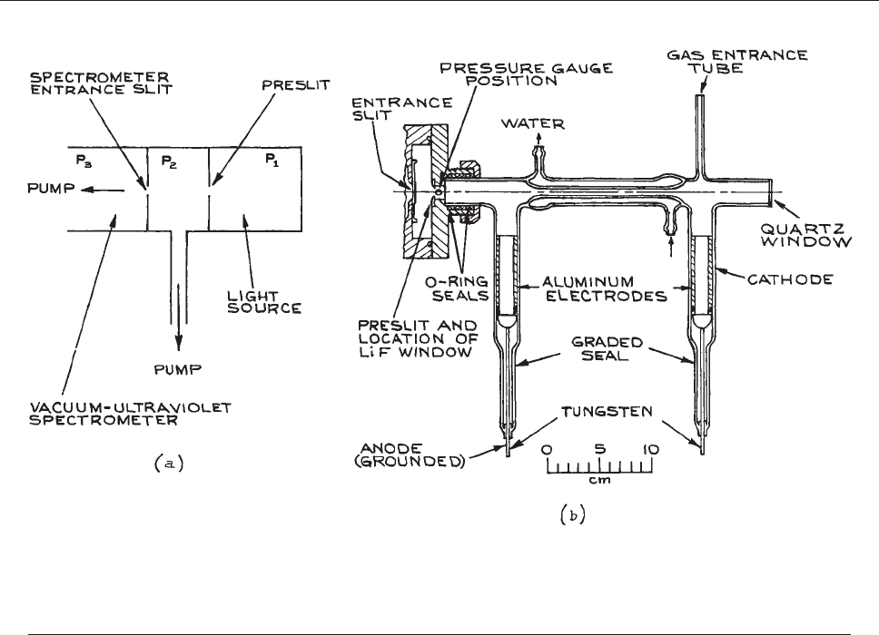
pump, as shown in Figure 4.112. This technique is called
differential pumping (see Section 3.6.2). For further
de
tails of vacuum-ultraviolet sour ces and technolog y,
thereaderisreferredtoSamson.
62
Microwave Lamps. Small microwave-driven
discharge lamps are very useful where a low-power
atomic-emission line source is desired, particularly if the
atomic emission is desired from some reactive species
such as atomic chlorine or iodine. A small cylindrical
quartz cell containing the material to be excited, usually
with the addition of a buffer of helium or argon, is excited
by a microwave source inside a small tunable microwave
cavity, as shown in Figure 4.113. Suitable cavities for this
purpose,
designed for operation at 2450 MHz, are
available from Opthos Instruments; power supplies for
these lamps are available from Opthos and Cathodeon.
Flashlamps. The highest-brightness incoherent radiation
is obtained from short-pulse flashlamps. By discharging a
capacitor through a gas-discharge tube, much higher
discharge currents and input powers are possible than in
d.c. operation. As the current density or pressure of a
flashlamp is increased, the emission from the lamp shifts
from radiation that is characteristic of the fill gas, with
lines superimposed on a continuum, to an increasingly
close approximation to blackbody emission corresponding
to the temperature of the discharge gas. Commercial
flashlamps can be roughly divided into two categories. In
long-pulse lamps, fairly large capacitors (100–10 000 lF),
Figure 4.112 (a) Differential pumping arrangement (P
1
, P
2
, P
3
are the light source, differential pumping unit, and
spectrometer operating pressures, respectively); (b) light source for the production of the noble-gas continua – in a
differentially pumped mode, no LiF window would be used. (From R. E. Huffman, Y. Tanaka, and J. C. Larrabee, ‘‘Helium
Continuum Light Source for Photoelectric Scanning in the 600–1100 A
˚
Region,’’ Appl. Opt., 2, 617–623, 1963; by
permission of the Optical Society of America.)
OPTICAL SOURCES 257
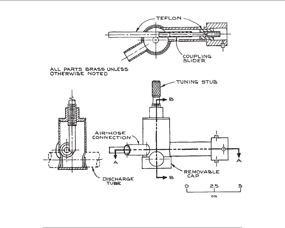
charged to moderately high v oltages (typically up to about 5
kV), are discharged slowly (on time scales from 100 lsto1
ms) through high-pressure discharge tubes. In short-pulse,
high-peak-power lamps, smaller , low-inductance capacitors
(typically 0.1–10 lF), charged to high voltages (10–80 kV),
are discharged rapidly (on time scales down to 1 ls) through
lower -pressure discharge tubes. Suppliers of linear
flashlamps include Continuum, Laser SOS Group, New
Source Technology, Perkin-Elmer Optoelectronics, and
Xenon Corporation.
(i) Long-pulse lamps. Long-pulse lamps are generally
filled with xenon,
63
but krypton lamps
64
(for pumping
Nd
3+
lasers) and alkali-metal lamps are also available. Fill
pressures are typically on the order of 0.1–1 bar. Although
the discharge current in such lamps can run to tens of
thousands of A/cm
2
, at low repetition frequencies (< 0.1
Hz) ambient cooling is all that is necessary. Three of the
most commonly used circuits for operating such lamps are
shown in Figure 4.114. In all three of these circuits, the
capacitor
, or pulse-forming network shown in Figure 4.114
(c), is charged through a resistor R.
The capacitor is dis-
charged through the lamp by triggering the flashlamp with
one of the trigger circuits shown in Figure 4.115. The lamp
itself
behaves both resistively and inductively when it is
fired. If the inductance and resistance of the lamp are not
Figure 4.113 Microwave cavity for exciting a gas discharge in a cylindrical quartz tube
(design used by Opthos). (After F. C. Fehsenfeld, K. M. Evenson, and H. P. Broida,
‘‘Microwave Discharge Cavities Operating at 2450 MHz,’’ Rev. Sci. Instr., 36, 294–298,
1965; by permission of the American Institute of Physics.)
258 OPTICAL SYSTEMS

Figure 4.114 Operating circuits for flashlamps (a ¼ lamp
anode; k ¼ lamp cathode): (a) RC discharge; (b) RLC
critically damped discharge; (c) pulse-forming network.
Figure 4.115 Flashlamp triggering schemes
(a ¼ lamp anode; k ¼ lamp cathode): (a) overvoltage trig-
gering (V > self-flash voltage of flashlamp; switching is
accomplished in this case with a
thyratron, but a triggered spark gap or ignitron can also be
used); (b) series triggering (a saturable
transformer is used with a fast-risetime 10–20 kV pulse with
sufficient energy to trigger the lamp and saturate the core);
(c) external triggering (the
flashlamp is ionized by a trigger wire wrapped around the
outside of the lamp and connected to the 5–15 kV
secondary of a high-voltage pulse transformer).
OPTICAL SOURCES 259
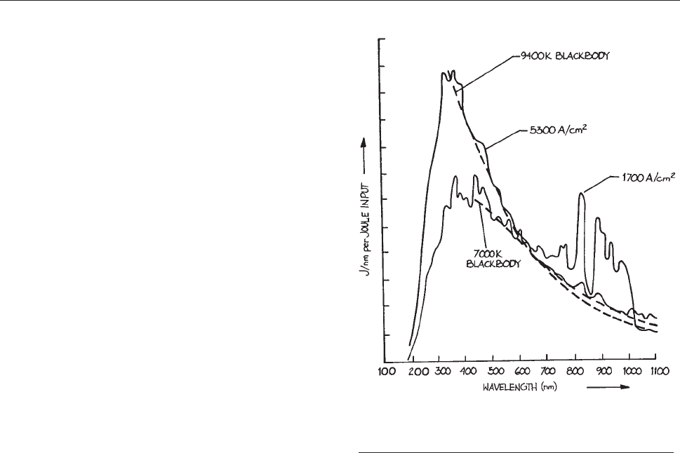
sufficiently large, the capacitor may discharge too rapidly,
which can lead to damage of both lamp and capacitor.
Generally speaking, an additional series inductor will be
desirable to control the discharge. The problem of select-
ing the appropriate inductor for a particular capacitor size
and lamp has been dealt with in detail by Markiewicz and
Emmett.
65
Slow flashlamps have a nonlinear V-I character-
istic, which can be approximated by:
V ¼ K
0
ffiffiffiffiffi
jIj
p
ð4:214Þ
where the sign of V is taken to be the same as the sign of I.
The value of K
0
, measured in X A
1/2
, is a parameter speci-
fied by a manufacturer for a given lamp. Given this value
and the capacitor size to be used, the calculations of Mar-
kiewicz and Emmett allow a suitable value of series induc-
tor to be chosen. Other factors must be taken into account
in designing the flashlamp circuit: the maximum power
loading, usually specified as the explosion energy of the
lamp (which will depend on the discharge-pulse duration),
and the maximum repetition frequency of the lamp. Usu-
ally, the larger the capacitor-stored energy, the lower the
permitted repetition frequency will be. As lamps and dis-
charge energies get smaller, repetition frequencies can be
extended, to several kilohertz for the smallest low-energy
lamps, such as those used in stroboscopes. The explosion
energy of the lamp is the minimum input required to cause
lamp failure in one shot. To obtain long flashlamp life, a
lamp should be operated only at a fraction of its explosion
energy. For example, at 50% of the explosion energy
the expected lifetime is from 100 to 1000 flashes, while
at 20% it is from 10
5
to 10
6
flashes. The lamp should be
mounted freely and not clamped rigidly at its ends when it
is operated.
The spectral output of a flashlamp varies slightly during
the flash. For moderate- and high-power lamps (> 100 J in 1
ms), the spectral output approaches that of a blackbody, as
shown in Figures 4.116 and 4.117.
66
Low-power lamps
exhibit the spectral feature of their fill gas, as shown in
Figure 4.118. Figure 4.116 shows the transition from a spec-
t
rum with some line structure to a blackbody continuum as
the current density through the lamp is increased.
A word about the triggering schemes shown in Figure
4.115. External triggering, accomplished by switching a
high-v
oltage pulse from a transformer to a trigger wire
wrapped around the lamp, is perhaps the simplest scheme;
it is used only with long-pulse lamps and does not give
quite so good time synchronization as series-spark-gap or
thyratron-switched operation. The other methods are more
complex, but can be also used with short-pulse, high-
power lamps. Series triggering allows the incorporation
of triggering and lamp series inductance in a single unit.
Trigger transformers of various types are available from
EG&G and ILC. EG&G and EEV supply a range of excel-
lent thyratrons.
(ii) Short-pulse high-power lamps. Flashlamps that can
handle the rapid discharge of hundreds of joules on time-
scales down to a few microseconds are available commer-
cially from Flashlamps (Verre et Quartz), ILC Technology,
Perkin Elmer, and Xenon Corporation, among others. To
achieve such rapid discharges, these lamps are generally
operated in a low-inductance discharge circuit. When these
lamps are fired at high-peak-power inputs, a severe shock
Figure 4.116 Output spectrum of a Perkin-Elmer FX-47A
xenon flashlamp (0.4 atm) at two current densities:
1700A/cm
2
and 5300A/cm
2
.
260 OPTICAL SYSTEMS
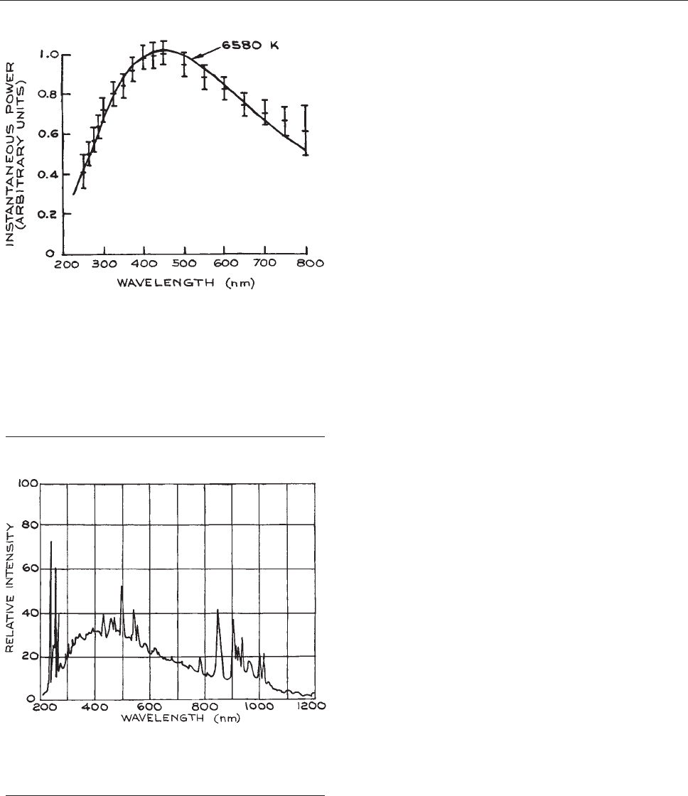
wave is generated in the lamp. To withstand the shock
wave, the lamps are designed with special re-entrant elec-
trode seals. If lamps designed for long-pulse operation are
discharged too rapidly, their electrodes are quite likely to
break off because the electrode seals are not shock-
resistant.
The spectral emission of short-pulse, high-energy lamps
is generally quite close to that of a high-temperature black-
body, perhaps as hot as 30 000 K. The fill pressure in these
lamps is often lower than in long-pulse lamps, typically
from 0.1 to a few tens of millibars. The fill gas is usually
xenon, but other noble gases such as krypton or argon can
be used. If a short-pulse lamp has a narrow discharge-tube
cross-section, at high power inputs material can ablate
from the wall and a substantial part of the emission from
the lamp can come from this material. Such lamps can be
made with heavy-walled discharge-tube bodies of silica,
glass, or even Plexiglas. These lamps can be made fairly
simply. A good design described by Baker and King
67
is
illustrated in Figure 4.119. It can be operated in a non-
ablating
or ablating mode (at high or low pressure, respec-
tively). When operated in the ablating regime, such lamps
can be filled with air as the nature of the fill gas is unim-
portant. Figure 4.119 also shows the use of a field-distor-
tion-triggered
spark gap for firing the lamp – a spark-gap
design that offers quiet, efficient switching of rapid-
discharge capacitors. Rapid-discharge (low-inductance)
capacitors suitable for fast flashlamp and other applica-
tions are available from CSI Technologies, Hipotronics,
and Maxwell Energy Products.
4.6 LASERS
Lasers are now so widely used in physics, chemistry, the
life sciences, and engineering that they must be regarded as
the experimentalist’s most important type of optical
source. With few exceptions, anyone who wants a laser
for an experiment should buy one. This is certainly true
in the case of helium–neon, argon–ion, and helium–
cadmium gas lasers and all solid-state crystalline, glass,
or semiconductor lasers. True, these lasers can be built in
the laboratory, but this is the province of the laser specialist
and will generally be found time-consuming and unpro-
ductive for scientists in other disciplines. On the other
hand, there are some lasers, such as nitrogen, Exciplex,
Figure 4.118 Spectral distribution of intensity from an
ILC 4L2 xenon flashlamp (51 mm long by 4 mm bore)
operated in a critically damped mode with 10 J discharged
in 115 ls. (Courtesy of ILC).
Figure 4.117 Spectral distribution of power radiated by an
EG&G FX42 xenon-filled flashlamp (76 mm long by 7 mm
bore) operated in a critically damped mode with 500 J
discharged in 1 ms. The spectral distribution was observed
0.7 ms from flash initiation. The line is the blackbody
radiation curve of best fit. (After J. G. Edwards, ‘‘Some
Factors Affecting the Pumping Efficiency of Optically
Pumped Lasers,’’ Appl. Opt., 6, 837–843, 1967; by per-
mission of the Optical Society of America.)
LASERS 261
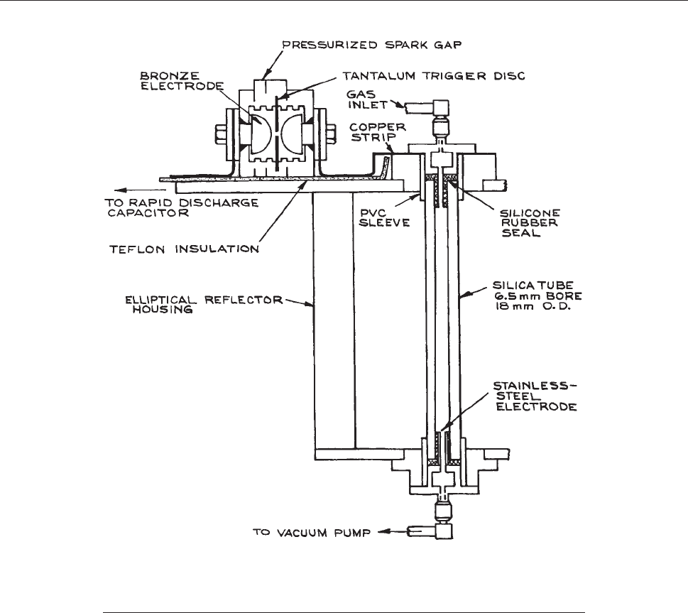
CO
2
, and CO gas lasers, and dye lasers, that it might occa-
sionally pay to build for oneself, even though models are
available commercially. A detailed discussion of how to
construct all these lasers will not be given here, but, to
illustrate how it is accomplished, design features of some
specific systems will be discussed.
Table 4.8 lists the primary wavelengths available from
the
more commonly used lasers presently available com-
mercially. For more detailed information about suppliers
and specifications consult a trade reference, such as the
Laser Focus or Photonics Spectra Buyers Guides. Laser
suppliers come and go, as does the availability of specific
types of laser. Before briefly describing some of these laser
systems, some background material will be presented that
is pertinent to a discussion of lasers in general. More
detailed information regarding the physics of laser opera-
tion is given in the books by Davis,
15
Silfvast,
68
Saleh and
Teich,
69
Yariv,
14
and Siegman.
70
Figure 4.119 High-pulse-energy, fast flashlamp design for conventional or
ablation-mode operation. (From H. J. Baker and T. A. King, ‘‘Optimization of Pulsed UV
Radiation from Linear Flashtubes,’’ J. Phys. E.: Sci. Instr., 8, 219–223, 1975. Copyright 1975
by the Institute of Physics, used with permission).
262 OPTICAL SYSTEMS

Table 4.8 Wavelengths available from important lasers
CW Gas Lasers
Type Operating Wavelengths (nm)
Ar ion 229
244
a
348
a
257
a
275
a
333.4
333.6
351.1
b
363.8
b
454.5
457.9
465.8
476.5
488.0
b
496.5
50.17
514.5
b
528.7
1092.3
Kr ion 337.5
350.7
356.4
406.7
413.1
461.9
468.0
476.2
482.5
530.9
b
568.1
b
647.0
676.4
752.5
793.1
799.3
He–Ne 543
594.1
612
632.8
c
1152
3392
5400
11552
He-Cd 325.0
441.6
CO 5–6.5
d
CO
2
9–11
d
10.6
e
LASERS 263

Pulsed Gas Lasers
Type Operating Wavelengths (nm)
Excimer
ArF 193.3
KrF 248.4–249.1
XeCl 307–308.43
XeF 348.8–354
Cu vapor 510.54
570
578.2
F
2
157
N
2
337.1
Type Operating Wavelengths (lm)
CO
2
10.6
9–11
CW Solid-State Lasers
Type Operating Wavelengths (lm)
Alexandrite 365
0.370
0.730
0.760
Nd:YAG 266.8
f
355
g
0.532
h
1.064
(This is the primary line, Nd:YLF gives 1.047 lm and 1.053 lm,
Nd:YVO4 also gives 1064 nm)
1.318
Ti:Sapphire 0.7–1.02
Tunable
Pulsed Solid-State Lasers
Type Operating Wavelengths (lm)
Alexandrite 0.720–0.780 (tunable, can also provide 2nd, 3rd and 4th harmonic wavelengths)
Er:fiber lasers 1.2–2.0
Er:glass 1.534
Er:YAG 2.940
Er:glass 1.534
Ho:YAG 2.1
Nd:glass 0.266
f
0.355
g
0.532
h
1.06
i
Table 4.8 (cont.)
264 OPTICAL SYSTEMS

Ti:Sapphire 0.68–1
Tunable
Nd:YAG 0.213
j
0.265
f
0.355
g
0.53
h
1.064
Ruby 0.6943
Ytterbium:glass 1.030
Diode-Pumped Solid-State Lasers
Type Operating Wavelengths (nm)
266
f
355
g
460
473
488
515
532
670
1064
1030
1480
1535–1565
CW Tunable Dye Lasers
(pumped with ion lasers, frequency-doubled Nd:YAG lasers at 530nm, or frequency tripled Nd:YAG laser at 355 nm)
Tuning range (lm)
0.4–1.1 (The tuning range depends on the dye used. A typical dye provides 50–100 nm of tuning)
Pulsed Tunable Dye Lasers
Tuning Range (lm)
0.197–1.036
a
Produced by second harmonic generation of blue-green argon ion laser lines.
b
Strongest lines.
c
Most readily available wavelength.
d
Molecular lasers that offer discrete tunability over several lines.
e
Strongest line. Industrial CO
2
lasers generally operate only at 10.6 lm.
f
Frequency quadrupled from 1.06 lm output.
g
Frequency tripled from 1.06 lm output.
h
Frequency doubled from 1.06 lm output.
i
Phosphate glass gives 1.05 lm. Nd:YLF gives 1.053 lm
j
Fifth harmonic from1.06 lm output.
Table 4.8 (cont.)
Pulsed Solid-State Lasers (Cont.)
Type Operating Wavelengths (lm)
LASERS 265

The lasers listed in the table fall into two categories:
pulsed and CW (continuous wave). Many can be operated
in both ways, with the exception of nitrogen, copper v apor,
andexcimerlasers,whichcanonlyoperateinapulsedmode.
These three laser types are self-terminating: once they lase
they destroy their own population inversio n, and a period of
time must elapse before the upper laser lev el can be re-excited.
For pulsed lasers, the available energy outputs per
pulse can be c lassified as low (< 10 mJ) medium (10
mJ–1 J), high ( 1 J–100 J), and very high (> 100 J). Pulse
lengths depend on the type of laser and its mode of oper-
ation. Almost all pulsed solid-state lasers operate in a Q-
switched mode,
15
which typically provides a pulse length
in the 10 ns range, bu t varies somewhat from man ufac-
turer to manufacturer. Non Q-switched long-pulse (LP)
solid-state lasers have pulse lengths > 0.1 ms. Solid-state
anddyelasersarefrequentlyoperatedinamode-locked
(ML) configuration, which provides pulse lengths in the
0.1–10 p s ra nge. A given las er can often be operated in
ML, Q, and LP modes. The energy output per pulse will
decrease as LP > Q > ML.
Continuous wave lasers can be classified by output
power as low (< 10 mW), medium (10 mW–1 W), high
(1–10 W), very high (10–100 W), and industrial (> 100 W).
Continuous wave gas lasers, in particular, provide power
outputs at many different wavelengths, and the available
power varies from line to line. These lasers are generally
supplied to operate in a specific wavelength range with
discrete tunability within that range. Ultraviolet gas lasers,
for example, are equipped with special optics, so do not
generally operate in the visible range as well.
The energy outputs available from pulsed lasers,
together with their available pulse-repetition rates and
pulse lengths, cover a very wide range. The highest
available energy outputs are generally available only
at the lowest pulse-repeti tion rates. In the ca se of CW
lasers, available power o utputs vary from line to line and
from manufacturer to manufacturer. To the intended pur-
chaser of a laser system, we recommend the following
questions:
(1) What fixed wavelength or wavelengths must the laser
supply?
(2) Is tunability required?
(3) What frequency and amplitude stability are required?
(4) What laser linewidth is required?
(5) What power or pulse energy is required?
(6) Are high operating reliability and long operating life-
time required?
(7) For time-resolved experiments, what pulse length is
needed?
(8) Is the spatial profile of the output beam important?
The desirable attributes in each of these areas are
unlikely to occur simultaneously. For example, frequency
tunability is not readily available throughout the spectrum
without resorting to the specialized techniques of nonlinear
optics.
14,15,71–75
In Table 4.8 the various categories of laser: CW gas,
pulsed gas, CW solid-state, pulsed solid state, CW dye
and pulsed dye frequently show tuning ranges and wave-
lengths that are obtained from these lasers by the use of
nonlinear optics. For example, shorter wavelengths from
argon ion, Nd:YAG, Ti:sapphire, and CO
2
can be obtained
by frequency doubling (tripling or even quadrupling) by
the use of a nonlinear crystal. The nonlinear crystal is
generally external to the primary laser, although it may
be housed in its own resonant structure. Generating second
or third harmonic light from a sufficiently powerful laser is
not especially difficult, although this is still a relatively
specialized endeavor.
New frequency generation from a primary pump laser
can also be obtained by the use of an optical paramatic
oscillator (OPO). In such a device an appropriate nonlinear
crystal is pumped with a frequency m
p
and in this process
generates two new frequencies m
s
and m
i
, called the signal
and idler frequencies, respectively. In this process photon
energy must be conserved, so:
m
p
¼ m
s
þ m
i
ð4:215Þ
High-energy and high-power lasers are generally less sta-
ble, both in amplitude and in frequency, and will generally
be less reliable and need more ‘‘hands on’’ attention than
their low-energy or low-power counterparts. When a deci-
sion is made to purchase a laser system, compare the spec-
ifications of lasers supplied by different manufacturers;
discuss the advantages and disadvantages of different sys-
tems with others who have purchased them previously.
Reputable laser manufacturers are generally very willing
to supply the names of previous purchasers.
266 OPTICAL SYSTEMS
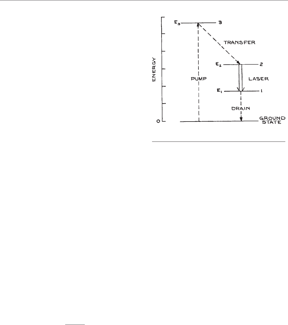
To some experimental scientists a laser is merely a
rather monochromatic directional lightbulb; for others,
detailed knowledge of its operating principles and charac-
teristics is essential. Certain aspects of laser designs and
operating characteristics, however, are very general and
are worthy of some discussion.
4.6.1 General Principles of Laser Operation
A laser is an optical-frequency oscillator: in common with
electronic circuit oscillators, it consists of an amplifier
with feedback. The optical-frequency amplifying part of
a laser can be a gas, a crystalline or glassy solid, a liquid, or
a semiconductor. This medium is maintained in an ampli-
fying state, either continuously or on a pulsed basis, by
pumping energy into it appropriately. In a gas laser the
input energy comes from electrons (in a gas discharge or
an electron beam), or from an optical pump (which may be
a lamp or a laser). Solid-state crystalline or glassy lasers
receive their pumping energy from continuous or pulsed
lamps, and in more and more cases from semiconductor
lasers. Liquid lasers can be pumped with a flashlamp or, on
a continuous or pulsed basis, by another laser. Semicon-
ductor lasers are p-n junction devices and are operated by
passing pulsed or continuous electrical currents though
them.
The amplifying state in a laser medium results if a pop-
ulation inversion can be achieved between two sublevels of
the medium. The energy sublevels of a system are single
states with their own characteristic energy. A set of sub-
levels having the same energy is called an energy level.
This can be seen with reference to Figure 4.120, which
sho
ws a schematic partial energy-level diagram of a typi-
cal laser system. Input energy excites ground-state par-
ticles (atoms, molecules, or ions) of the medium into the
state (or states) indicated as 3. These particles then transfer
themselves or excite other particles preferentially to sub-
level 2. In an ideal system, negligible excitation of par-
ticles into sublevel 1 should occur. If the populations of the
sublevels 2 and 1 are n
2
and n
1
, respectively, and n
2
> n
1
,
this is called a population inversion. The medium then
becomes capable of amplifying radiation of frequency:
v ¼
E
2
E
1
h
ð4:216Þ
where h is Planck’s constant. In practice, energy levels of
real systems are of finite width, so the medium will amplify
radiation over a finite bandwidth. The gain of the amplifier
varies with frequency in this band and is specified by a gain
profile g(v), as shown in Figure 4.121. Actual laser oscil-
lation
occurs when the amplifying medium is placed in an
optical resonator, which provides the necessary positive
feedback to turn the amplifier into an oscillator. Most opti-
cal resonators consist of a pair of concave mirrors, or one
concave and one flat mirror, placed at opposite ends of the
amplifying medium and aligned parallel. A laser resonator
is in essence a Fabry–Perot (see Section 4.7.4), generally
of
large spacing. The radii and spacing of the mirrors will
determine, to a large degree, the type of Gaussian beam
that the laser will emit. At least one of the mirrors is made
partially transmitting, so that useful output power can be
extracted. The choice of optimum mirror reflectance
depends on the type of laser and its gain.
Low-gain lasers such as the helium–neon have high-
reflectance mirrors, (98–99%), while higher-gain lasers
such as pulsed nitrogen, CO
2
,orNd
3+
:YAG can operate
with much lower reflectance values. In certain circumstan-
ces, when their gain is very high, lasers will emit laser
radiation without any deliberately applied feedback.
Figure 4.120 Schematic partial energy-level diagram of a
laser system.
LASERS 267
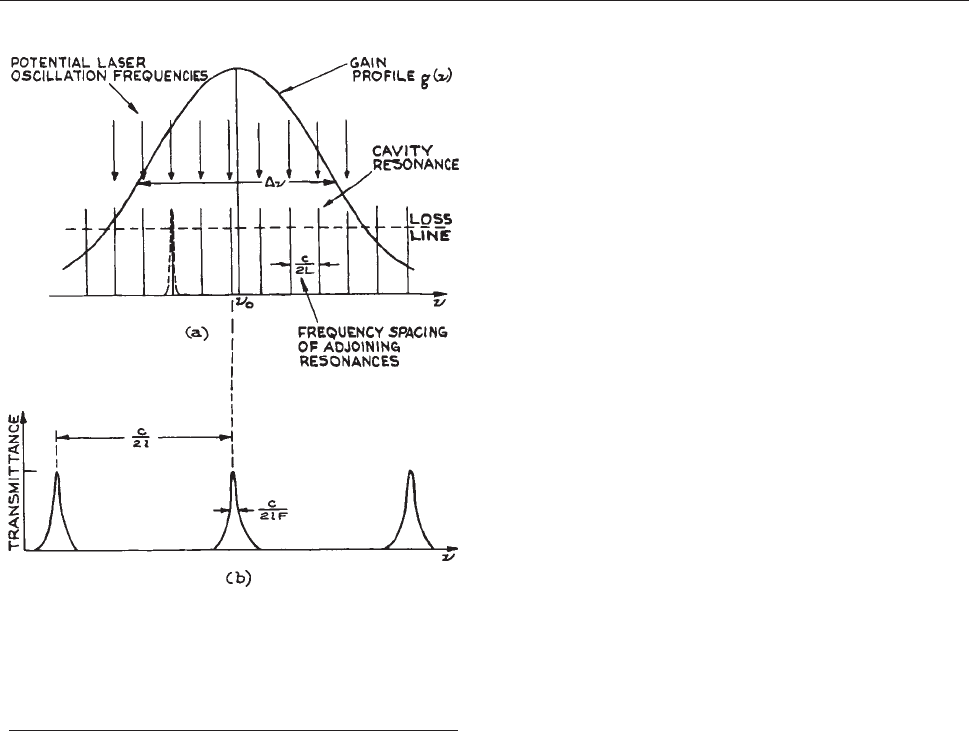
Lasers that operate in this fashion are generally operating
in an amplified spontaneous emission (ASE) mode. Such
lasers are just amplifying their own spontaneous emission
very greatly in a single pass.
4.6.2 General Features of Laser Design
Even though the majority of laser users do not build their
own, an awareness of some general design features of laser
systems will help the user to understand what can and
cannot be done with a laser. It will also assist the user
who wishes to make modifications to a commercial laser
system to increase its usefulness or convenience in a par-
ticular experimental situation. Figure 4.122 shows a sche-
matic
diagram of a typical gas laser, which incorporates
most of the desirable design features of a precision system.
The amplifying medium of a gas laser is generally a high-
or low-pressure gas excited in a discharge tube. The exci-
tation may be pulsed (usually by capacitor discharge
through the tube), d.c., or occasionally a.c. Some gas lasers
are also excited by electron beams, by radiofrequency
energy, or by optical pumping with either a lamp or
another laser. Far-infrared lasers, in particular, are fre-
quently pumped with CO
2
lasers. Depending on the cur-
rents that must be passed through the discharge tube of the
laser, it can be made of Pyrex, quartz, beryllium oxide,
graphite, or segmented metal. These last three have been
used in high-current-density discharge tubes for CW ion
lasers. Several types of pulsed high-pressure or chemical
lasers, such as CO
2
, HF, DF, and HCI, can be excited in
structures built of Plexiglas or Kel-F.
Because most gas lasers are electrically inefficient, a
large portion of their discharge power is dissipated as heat.
If ambient or forced-air cooling cannot keep the discharge
tube cool enough, water cooling is used. This can be done
in a closed cycle, using a heat exchanger. Some lasers need
the discharge tube to run at temperatures below ambient. In
such cases a refrigerated coolant such as ethylene glycol
can be used. Many gas lasers use discharge tubes fitted
with windows placed at Brewster’s angle. This permits
linearly polarized laser oscillation to take place in the
direction indicated in Figure 4.122; light bouncing back
and
forth between the laser mirrors passes through the
windows without reflection loss. Mirrors fixed directly
on the discharge tube can also be used – this is common
in commercial He–Ne lasers. In principle, such lasers
should be unpolarized, although in practice various slight
anisotropies of the structure often lead to at least some
polarization of the output beam. The two mirrors that con-
stitute the laser resonator, unless these are fixed directly to
the discharge tube, should be mounted in kinematically
designed mounts and held at fixed spacing ‘ by a thermally
stable resonator structure made of Invar or quartz. In this
structure an important parameter is the optical length, L,of
the structure. For a laser in which the whole space between
the two resonator mirrors is filled with a medium of refrac-
tive index n, the optical length is L ¼ n‘. For a composite
structure with regions of different refractive index this
result is easily generalized. Because the laser generates
one or more output frequencies which are close to integral
Figure 4.121 (a) Laser gain profile showing position of
cavity resonances and potential laser oscillation frequencies
near cavity resonances where gain lies above loss (L is length
of laser cavity); (b) transmission characteristic of intracavity
etalon, on same frequency scale as (a), for single-mode
operation (l is the etalon thickness and F its finesse).
268 OPTICAL SYSTEMS
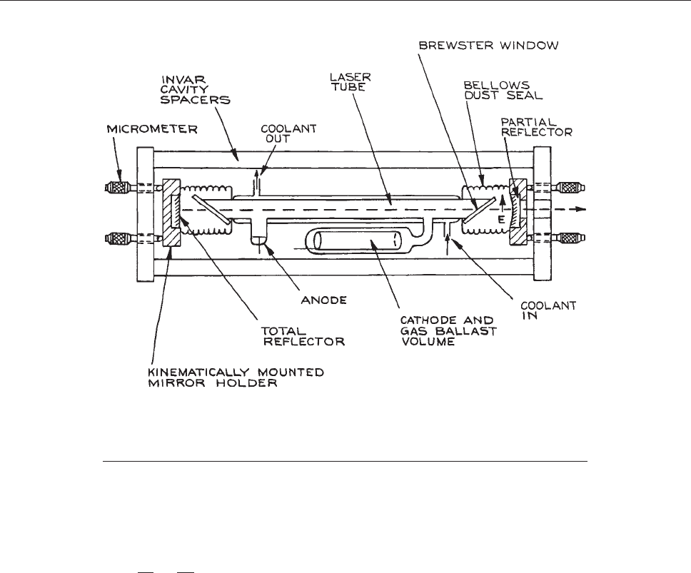
multiples of c/2L, any drift in mirror spacing L causes
changes in output frequency v. This frequency change Dv
satisfies:
Dm
m
¼
DL
L
ð4:217Þ
For a laser 1 m long, even with an Invar-spaced resonator
structure, the temperature of the structure would need to be
held constant within 10 mK to achieve a frequency stabil-
ity of only 1 part in 10
8
. The discharge tube should be
thermally isolated from the resonator structure unless the
whole forms part of a temperature-stabilized arrangement.
If single-frequency operation is desired, the laser should
be made very short – so that c/2L becomes larger than Dv in
Figure 4.121 – or operated with an intracavity etalon (see
Sections 4.6.4 and 4.7.4). Visible lasers that have the capa-
bility
of oscillating at several different wavelengths are
generally tuned from line to line by replacing one laser
mirror with a Littrow prism whose front face is set at
Brewster’s angle and whose back face is given a high-
reflectance coating, as shown in Figure 4.123(a). Alterna-
ti
vely, as shown in Figure 4.123(b), one can use a separate
intracavity
prism, designed so the intracavity beam passes
through both its faces at Brewster’s angle. Infrared gas
lasers that can oscillate at several different wavelengths
are tuned by replacing one resonator mirror with a gold-
coated or solid metal diffraction grating mounted in Lit-
trow, as shown in Figure 4.123(c). The laser oscillation
wav
elength then satisfies:
mk ¼2d sin h ð4:218Þ
where d is the spacing of the grating grooves, h is the angle
of incidence, and m is an integer.
A laser will oscillate only if its gain exceeds all the
losses in the system, which include mirror transmission
losses, absorption and scattering at mirrors and windows,
Figure 4.122 Schematic diagram of a typical gas laser showing some of the desirable
features of a well-engineered research system. In high-discharge-
current systems, some form of internal or external gas-return path from cathode to anode
must be incorporated into the structure.
LASERS 269
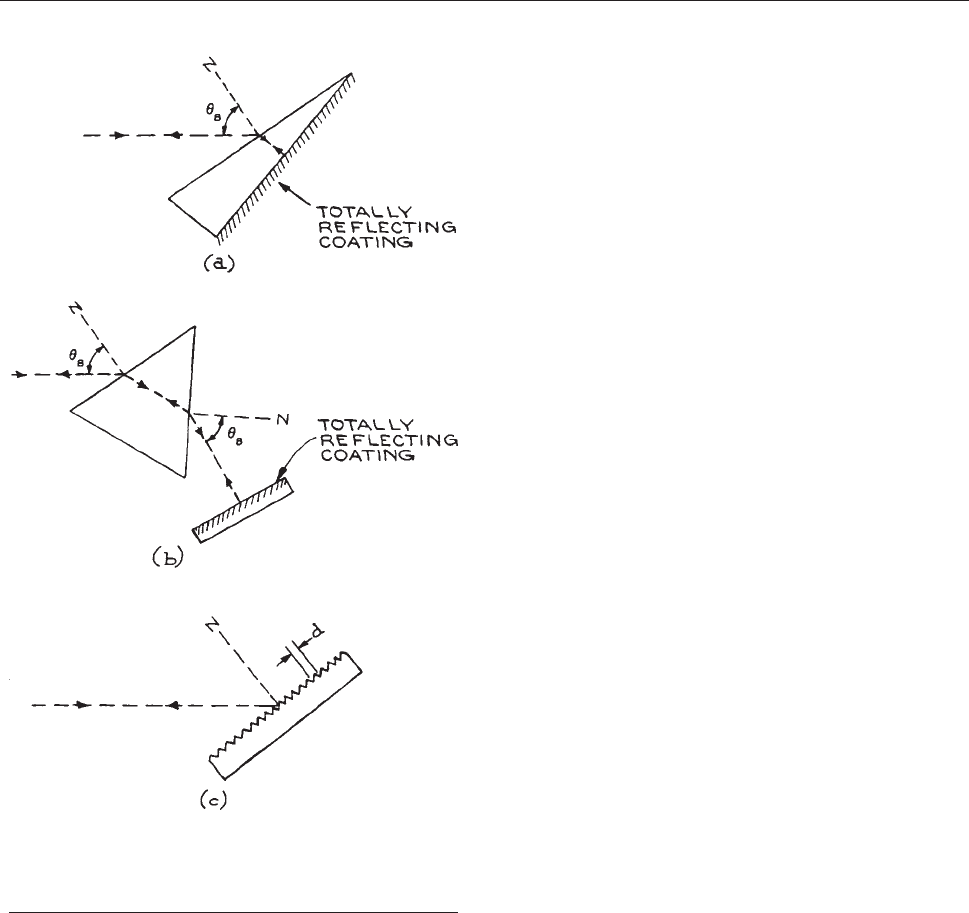
and any inherent losses of the amplifying medium itself –
the last generally being significant only in solid-state,
liquid, and semiconductor lasers. Consequently, it is par-
ticularly important to keep the mirrors and windows of a
laser system clean and free of dust. Most commercial sys-
tems incorporate a flexible, sealed enclosure between
Brewster windows and mirrors to exclude contaminants.
Figure 4.124 shows some design features of a simple
lamp-pumped
solid-state laser oscillator. This design
incorporates a linear pulsed or continuous lamp and a
crystalline or glass laser rod with Brewster windows
mounted inside a metal elliptical reflector, which serves
to reflect pumping light efficiently into the laser rod.
Although such solid-state lasers are rarely used in experi-
ments where extreme frequency stability and narrow line-
width operation are required, it is still good practice to
incorporate features such as stable, kinematic resonator
design and thermal isolation of the hot lamp from the
resonator structure. Elliptical reflector housings for solid-
state lasers (and flashlamp-pumped dye lasers) can be
made in two halves by horizontally milling a rectangular
aluminum block with the axis of rotation of the milling
cutter set at an angle of arccos(a/b), where a and b are the
semiminor and semimajor axes of the ellipse. This process
is repeated for a second aluminum block. The two halves
are then given a high polish, or plated, and joined together
with locating dowel pins. For further details of solid-state
laser design and particulars of other arrangements for opti-
cal pumping the reader should consult Ro
¨
ss
76
or Koech-
ner.
77
Flashlamp-pumped dye lasers share some design
features with solid-state lasers. The main difference is that
the former require excitation of short pulse duration
(< 1 ls) with special flashlamps in low-inductance dis-
charge circuitry.
78–81
4.6.3 Specific Laser Systems
Gaseous Ion Lasers. Gaseous ion lasers, of which the
argon, krypton, and helium–cadmium are the most impor-
tant, generate narrow-linewidth, highly coherent visible
and ultraviolet radiation with powers in the range from
milliwatts to a few tens of watts CW. Pulsed ion lasers
operate at high current densities, but have low duty cycles,
so that ambient cooling is adequate. These lasers are not in
widespread experimental use. Helium–cadmium lasers use
low-current-density (a few A/cm
2
) air-cooled discharge
structures, which in many respects are similar to those of
helium–neon lasers. They are limited to a few tens of milli-
watts in conveniently available output power. They do,
however, provide UVoutput at 325 nm. Argon and krypton
ion lasers use very high-current-density discharges (100–
2000 A/cm
2
) in special refractory discharge structures
Figure 4.123 Methods for wavelength-selective reflection
in laser systems: (a) Brewster’s-angle Littrow prism; (b)
intracavity Brewster’s-angle prism; (c) reflective diffraction
grating. N ¼ surface normal.
270 OPTICAL SYSTEMS
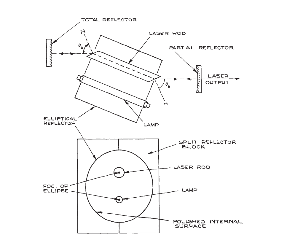
usually made of tungsten disks with ceramic spacers, as
shown in Figure 4.125. In operation, these disks cool them-
selves
by radiating through an outer fused-silica envelope
surrounded by coolant water. Commercially available
powers range up to a few tens of watts, but outputs up to
1 kW in the visible have been reported. Low power (< 100
mW) argon ion lasers can be forced-air cooled. Compre-
hensive information about ion lasers can be found else-
where.
82,83
Argon and krypton ion lasers are available
commercially from Coherent, JSC Plasma, JDSU, Melles
Griot, and Spectra Physics (Newport Corporation). Argon
and krypton ion lasers have in the past been widely used
for pumping CW dye lasers and Ti:sapphire lasers. They
are, however, rapidly being replaced in these applications
by frequency-doubled Nd lasers, which are more and more
likely to be pumped themselves by semiconductor diode
lasers. Because of the large currents at which they operate,
argon and krypton ion lasers regularly need their plasma
tubes to be replaced (typically evey few thousand hours of
operation), which is an expensive business. It appears
Figure 4.124 Schematic diagram of a simple solid-state laser system.
LASERS 271

likely that these lasers will disappear from use and be uni-
versally replaced by diode-pumped solid-state (DPSS) lasers.
Helium–Neon Lasers. Of all types of laser, helium–
neon lasers come closest to being the ideal classical mono-
chromatic source. They can have very good amplitude
(’ 0.1%) and frequency stability (1 part in 10
8
without
servo frequency control). Servo-frequency-controlled ver-
sions are already in use as secondary frequency standards,
and have excellent temporal and spatial coherence.
84
Typical available power outputs range up to 50 mW. Sin-
gle-frequency versions with power outputs of 1 mW, which
are ideal for interferometry and optical heterodyne experi-
ments, are available from Spectra-Physics and Aerotech.
Although 632.8 nm is the routinely available wavelength
from He–Ne lasers, other wavelengths, such as 543 nm or
1.15 or 3.39 lm are also available. Helium–neon lasers of
low power are very inexpensive, costing from about $100,
and are ideal for alignment purposes. Because of their
superior spectral qualities compared to semiconductor
lasers that can operate at the same wavelength, they remain
a valuable source in applications such as interferometry
and metrology. Other suppliers include Newport/Spectra
Physics, Meles Griot, and Micro-Controle.
Helium–Cadmium Lasers. These lasers are similar
in many ways to helium–n eon lasers. They operate at
relatively low current densities and use discharge tube
structures that do not require water cooling. They are
quite important in applications requiring deep blue and
ultraviolet light at powers of ten of milliwatts. They
operate at 325 nm and 441.6 n m. Th ese wavelengths,
especially 325 nm, are useful in applications where a
photochemically active source is require d. They are
widely used in photolithography. Helium–cadmium
lasers are available from Kimmon Electric Co. and
Melles Griot.
CO
2
Lasers. Both pulsed and CW CO
2
lasers are easy to
construct in the laboratory. A typical low-pressure CW
version would incorporate most of the features shown in
Figure 4.122. A water-cooled Pyrex discharge tube of
internal
diameter 10–15 mm, 1–2 m long, and operating
at a current of about 50 mA, is capable of generating tens
of watts output at 10.6 lm. The best operating gas mixture
is CO
2
–N
2
–He in the ratio 1:1:8 or 1:2:8, at a total pressure
of about 25 mbar in a 10 mm diameter tube. ZnSe is the
best material to use for the Brewster windows, as it is
transparent to red light and permits easy mirror
alignment. The optimum output mirror reflectance
depends on the ratio of the tube length to diameter, L/d,
roughly according to:
85
R ’ 1 L=500d ð4:219Þ
Figure 4.125 Construction of a high-power, water-cooled ion laser.
272 OPTICAL SYSTEMS

The output mirror is usually a dielectric-coated germa-
nium, gallium arsenide, or zinc selenide substrate. Such
mirrors are available from Janos, Laser Optics, Coherent,
Infrared Industries, Laser Research Optics, Unique Opti-
cal, and II-VI Infrared, and Rocky Mountain Instruments,
among others. The total reflector can be gold-coated in
lasers with outputs of a few tens of watts. For tunable
operation, gratings are available from American Holo-
graphic, Gentec, Jobin-Yvon, Perkin-Elmer, Richardson
Grating Laboratory, and Rochester Photonics. When a gra-
ting is used to tune a laser with Brewster windows, the
grating should be mounted so that the E vector of the laser
beam is orthogonal to the grating grooves. An excellent
review of low-pressure CW CO
2
gas lasers has been given
by Tyte.
85
Continuous wave CO
2
lasers can also be operated in a
waveguide configuration, in which a much higher pressure
gas mixture is excited in a small size discharge capillary.
86
These lasers provide substantially greater power output per
volume than the low pressure variety. They can be excited
by direct current, but r. f. excitation is now popular, and has
now solved the unreliability problems that afflicted early
commercial versions. Current suppliers of these compact
lasers are Access Laser, Coherent, Edinburgh Instruments,
Infrared Optical Products, Rofin-Sinar, Synrad, Trumpf,
and Universal Laser Systems.
Transversely excited atmospheric-pressure (TEA) CO
2
lasers ar e widely us ed when high-energy, pulsed infrared
energy near 10 lm is required. These lasers operate in
discharge structures w her e the current flow is transverse
to t he resonat or axis through a hig h- press ure (> 0.5 bar)
mixture of CO
2
,N
2
, and He, typically in the ratio 1:1:5.
To achieve a uniform, pulsed glow discharge through a
high-pressur e g as , special electro de structur es and pre-
ionization techniques are used to inhibit the formation
of locali zed spark discharges. Many very-high-energy
types utilize electron-beam excit ation. Discharge-excited
TEA lasers are relatively easy to construct in the labora-
tory. A device with a discharge volume 60 cm long 3 5
cm wide with a 3 cm electrode spacing excited with a 0.2
lF c apacitor charged to 30 kV, will generate several
joules in a pulse about 150 ns long. There a re very many
different d esigns for CO
2
TEA lasers; particulars of var-
ious ty pe s can be found in the IEEE Journ al of Quantum
Electronics and the Journal of Applied Physics. A partic-
ularly good design that is easy to construct is derived
from a vacuum-ultraviolet photopreionized design
described by Seguin and Tulip.
87
A diagram of the dis-
charge structure is shown in Figure 4.126 , together with
i
ts associated capacitor-dischargecircuitry.Thecathode
is an aluminum Rogowski 2p/3 profile;
88
the anode i s a
brass m esh, beneath which is a section of doub le -side d
copper-clad printed circuit board machined into a matrix
of separate copper sections on its top side. This printed
circuit b oard provides a source of very many surface
sparks for photopreion iza tion of the main discharge.
The laser is fitted with two separate capacitor banks: e ach
circuit-boa rd spark chan ne l is energized by a 3600 pF
Sprague or similar ‘‘doorknob’’ capaci tor, while the main
discharge is energized with a 0.2 lF low-inductance
capacitor. S uch capacitors ar e available from CSI Tech-
nologies, Hi Voltage Compon ents, and Maxwell Labs.
Both capacitor banks are switched with a s ingle spark
gap, which incorporates a Champion marine spark plug
for triggering. The end of the spark plug, which has an
annular gap, i s ground down to it s ceramic insulator and
is triggered by an EG&G Model TM-11A Trigger gener-
ator. A good double Rogowski TEA laser design has been
given by Seguin, Manes, an d Tulip.
89
TEA lasers based
on the multiple-pin-discharge design first described by
Beaulieu
90
arealsoeasytoconstruct,buttheydonotgive
output en ergies com para ble to those of volume-excited
designs. They do, however, lend themselves we ll to l aser
oscillation in many different gases – for example, HF
formed by discharge excitation of H
2
–F
2
mixtures.
CO Lasers. Continuous wave CO lasers are essentially
similar in construction to CO
2
lasers except that the dis-
charge tube must be maintained at low temperatures –
certainly below 0 °C. They operate in a complex mixture
of He, CO, N
2
,O
2
, and Xe with (for example) 21 mbar He,
0.67 mbar N
2
, 0.013 mbar O
2
, and 0.4 mbar Xe. They are
available from Access Laser and Edinburgh Instruments.
Exciplex (Excimer) Lasers. Exciplex lasers operate
in high-pressure mixtures such as Xe–F
2
, Xe–Cl
2
, Kr–Cl
2
,
Kr–F
2
, and Ar–F
2
. They are commonly also called ‘‘exci-
mer’’ lasers, although this is not strictly correct scientific
terminology except in the case of the F
2
*
laser. Both dis-
charge TEA and E-beam-pumped configurations are used.
LASERS 273
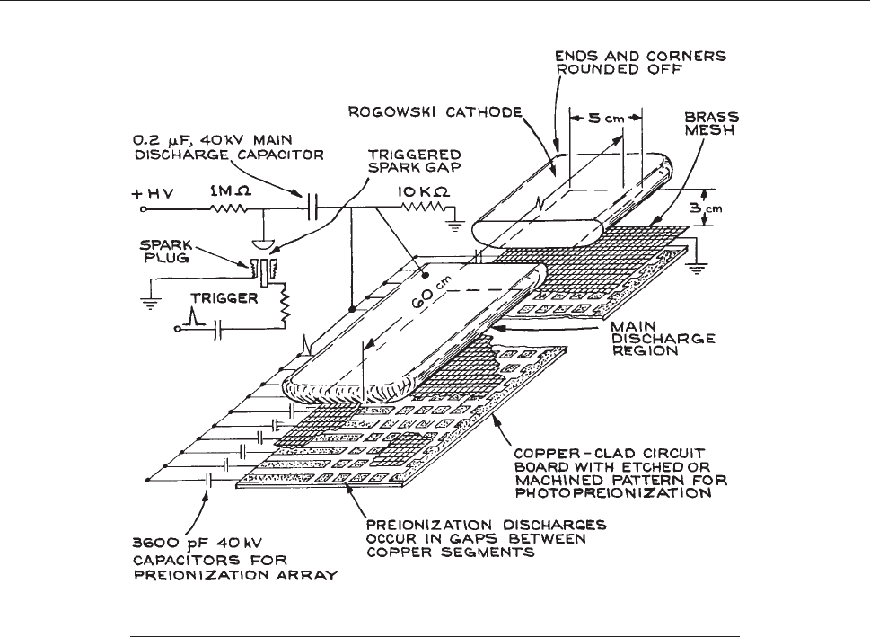
Under electron bombardment, a series of reactions occur
that lead to the formation of an excited complex (exciplex)
such as XeF
*
, which is unstable in its ground state and so
dissociates immediately on emitting light. Excimer lasers
available commercially are sources of intense pulsed ultra-
violet radiation. The radiation from these lasers is not
inherently of narrow linewidth, because the laser transition
takes place from a bound to a repulsive state of the exci-
plex, and therefore is not of well-defined energy. Excimer
lasers are attractive sources for pumping dye lasers and
whenever intense pulsed UV radiation is required in, for
example, photolithography or photochemistry.
The beam quality from an excimer laser is not normally
very high. These are ‘‘multimode’’ lasers, with often a
rectangular output beam profile. These lasers are widely
available commercially from companies such as Gam
Laser, JP Sercel Associates (JPSA), Lambda Physik
(now Coherent), Optec, MPB Communications, and
SOPRA.
Excimer lasers share technological design features in
common with both CO
2
TEA lasers and nitrogen lasers.
They use rapid pulsed electrical discharges through the
appropriate high-pressure gas mixture. The discharge
design must be of low inductance and the excitation is
generally faster than is necessary to operate a CO
2
TEA
laser. Because these lasers use toxic gases, such as fluorine
and chlorine, appropriate gas-handling safety precautions
must be taken in their use. The gases used, which are
usually diluted mixtures of a halogen in a noble gas, should
be housed in a vertical gas cabinet and exhaust gases from
the laser should be sent through a chemical ‘‘scrubber’’ or
filter cartridge before venting into the atmosphere.
Figure 4.126 Cutaway view of vacuum-ultraviolet photopreionized Rogowski TEA laser
structure.
274 OPTICAL SYSTEMS

Nitrogen (N
2
) Lasers. Molecular-nitrogen lasers are
sources of pulsed ultraviolet radiation at 337.1 nm. Com-
mercially available low-energy devices usually operate on
a flowing nitrogen fill at pressures of several tens of mbar,
and generate output powers up to about 1 MW in pulses up
to about 10 ns long. These lasers are reliable and easy to
operate, and are widely used for pumping low-energy
pulsed dye lasers. Nitrogen lasers, by virtue of their inter-
nal kinetics, only operate in a pulsed mode. They use very
rapid transversely excited discharges, usually between two
parallel, rounded electrodes energized with small, low-
inductance capacitors charged to about 20 kV. The whole
discharge arrangement must be constructed to have very
low inductance. Special care must be taken with insulation
in these devices; the very rapidly changing electric fields
present can punch through an insulating material to ground
under circumstances where the same applied d.c. voltage
would be very adequately insulated. There are several
good N
2
-laser designs in the literature.
91–96
These designs
fall into two general categories: Blumlein-type distributed-
capacitance discharge structures, and designs based on
discrete capacitors. The latter, although they do not give
such high-energy outputs from a given laser as the very
rapid-discharge Blumlein-type structures, are much easier
to construct in the laboratory and are likely to be much
more reliable. The capacitors used in these lasers need to
be of low inductance and capable of withstanding the high
voltage reversal and rapid discharge to which they will be
subjected. Suitable capacitors for this application can be
obtained from Murata or Sprague.
The output beam from a transversely excited N
2
laser is
by no means Gaussian. It generally takes the form of a
rectangular beam, typically ’ 0.5 cm 3 3 cm, with poor
spatial coherence. Such a beam can be focused into a line
image with a cylindrical lens for pumping a dye cell in a
pulsed dye laser. Nitrogen lasers are available commer-
cialy from LTB Lasertechnik and Spectr-Physics (now
Newport).
Copper Vapor Lasers. These are high-pulse-
repetition-frequency (prf) pulsed gas lasers that operate
using high-temperature gas mixtures of copper vapor in a
helium or neon buffer gas. With individual pulse energies
up to several millijoules and prf up to 20 kHz, these lasers
provide average powers up to several watts. They are used
for pumping pulsed dye lasers. The principal operating
wavelengths are 510.6 and 578.2 nm. Suppliers include
Laser Consultants and Oxford Laser. Pulsed gold vapor
lasers are also available commercially, which are similar
in most respects. They operate at 627.8 nm.
Continuous wave Solid-State Lasers. The most
important laser in this category is the Nd:YAG laser, where
YAG (yttrium aluminum garnet Y
3
Al
5
O
12
) is the host
material for the actual lasing species – neodymium ions,
Nd
3+
. Other host materials are also used: YLF (yttrium
lithium fluoride, LiYF
4
), YVO
4
(yttrium vanadate), YALO
(yttrium aluminum oxide YAlO
3
) and GSGG (scandium-
substituted gadolinium gallium garnet, Gd
3
Sc
2
Ga
3
O
12
).
The principal neodymium output wavelength is 1.06 lm,
but other infrared wavelengths, especially 1.32 lm, are
available. There are many suppliers.
31
The 1.06 lm can
be efficiently doubled to yield a CW source of green radi-
ation. This source of green radiation has replaced the
argon-ion laser in many applications, especially since the
neodymium laser itself can be pumped so conveniently
with appropriate semiconductor lasers.
Ti:sapphire is an attractive laser material for generating
tunable radiation in the 700–1060 nm range. These lasers
are generally pumped by argon-ion lasers on frequency-
doubled neodymium lasers. Suppliers include Coherent,
Inc., Continuuum, Photonics Industries International, and
Quantronix.
Fiber lasers use a gain medium that is a fiber doped with
rare-earth ions such as erbium (Er
3+
), neodymium (Nd
3+
),
ytterbium (Yb
3+
), thulium (Tm
3+
), or praseodymium
(Pr
3+
). They are pumped by one or more semiconductor
laser diodes.
97
A simple schematic of how they are con-
structed is shown in Figure 4.127. In practice, the pump
light
may be coupled in through the cladding of the fiber.
Very high-power fiber lasers with powers above 100 W are
increasingly being used in industrial applications. Suppli-
ers include B&W Tek, Fibercore, Fibertek, IPG Photonics,
Micro-Controle, Newport, Nufren, and Toptica. Fiber
lasers can be mode-locked to generate very short pulses
(< 1 ps) in the infrared. Pulsed Er
3+
fiber lasers are avail-
able from Calmar Optcom, PriTel, and IPG Phtonics.
Pulsed Yb
3+
lasers are available from Calmar Optcom,
Clark-MXR, IPG Photonics, Laser Photonics, and Quantel.
LASERS 275
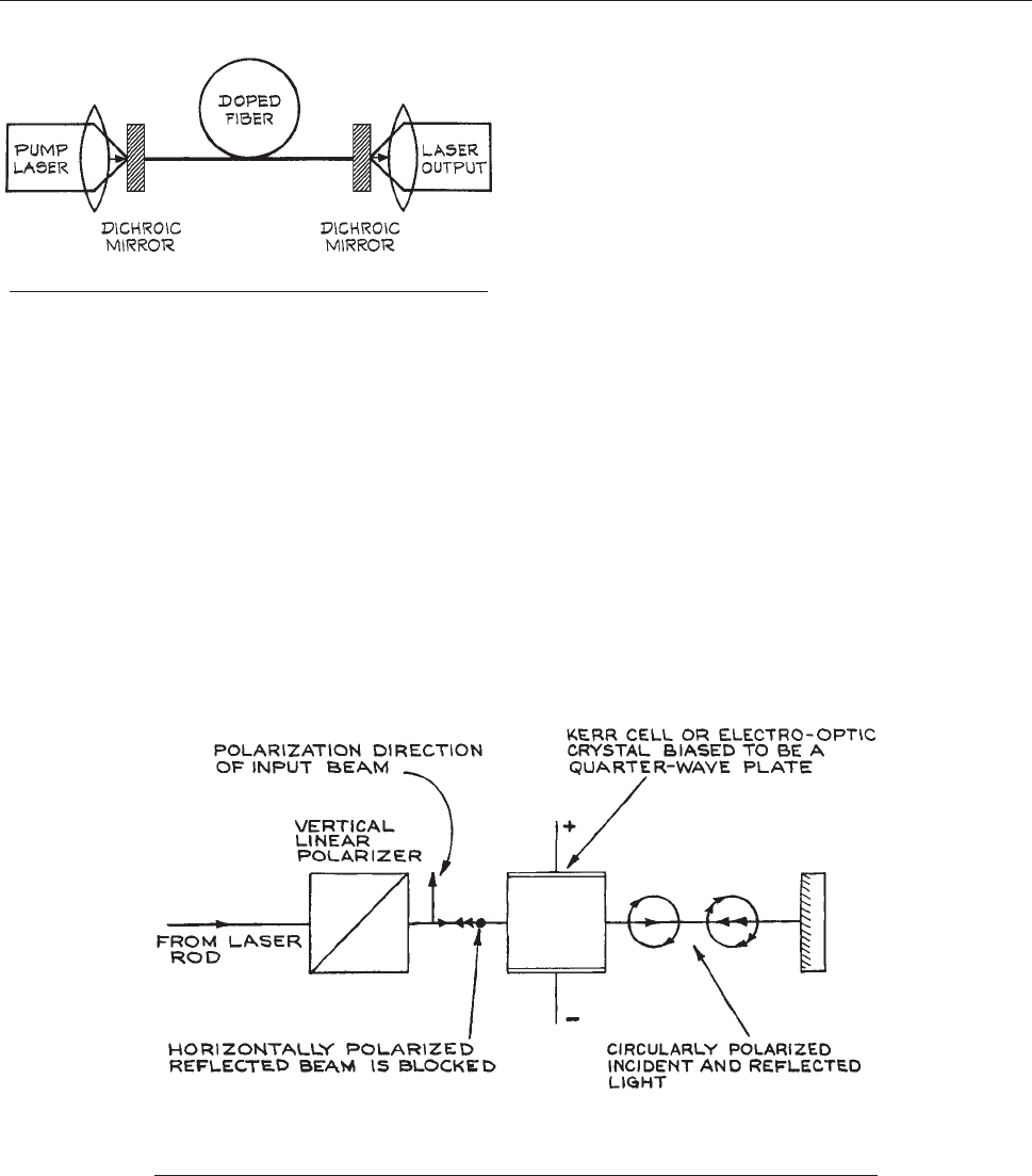
An important application of erbium-doped fiber is in
erbium-doped optical fiber amplifiers (EDFAs), widely
used in fiber optic communication networks to amplify
1.55 lm semiconductor laser radiation.
F-center lasers
98
are doped-crystal lasers that are pumped
with argon, krypton, or dye lasers. They pr ovide tunable
operation in two regions: between 1.43 and 1.58 lmand
between 2.2 and 3.3 lm, but are somewhat inconvenient,
because the crystal must be cooled with liquid nitrogen.
They no longer appear to be av ailable commercially .
Pulsed Solid-State Lasers. Three lasers are most
important in this category Nd:YAG, Nd:glass, and ruby.
Nd:YAG and Nd:glass lasers oscillate at the same principal
wavelength, 1.06 lm. Nd:YAG is generally used in high-
pulse-repetition-rate systems and/or where good beam
quality is desired. High-energy Nd laser systems frequently
incorporate an Nd:YAG oscillator and a series of Nd:glass
amplifiers. There are many suppliers.
31
Ruby lasers,
despite being the first laser to be demonstrated, are little
used in research. They have medical applications because
they provide a high-energy pulsed deep-red output (694.3
nm). They are available from Continuum.
All these pulsed solid-state lasers use fairly long flash
excitation (’ 1 ms). Unless the laser pulse output is con-
trolled, they generate a very untidy optical output, consist-
ing of several hundred microseconds of random optical
pulses about 1 ls wide, spaced a few microseconds apart.
This mode of operation, called spiking, is rarely used. Usu-
ally the laser is operated in a Q-switched mode. In this mode
the laser cavity is blocked with an optical shutter such as an
electro-optic modulator or Kerr cell, as illustrated in Figure
4.
128. An appropriate time after flashlamp ignition, after the
po
pulation inversion in the laser rod has had time to build to
a high value, the shutter is opened. This operation, which
changes the Q of the laser cavity from a low to a high value,
causes the emission of a very large short pulse of laser
energy. The Q-switched pulse can contain nearly as much
energy as would be emitted in the ‘‘spiking’’ mode and is
Figure 4.127 Schematic construction of a fiber laser.
Figure 4.128 Schematic arrangement for Q-switching. Laser oscillation occurs when the
voltage bias on the Kerr cell or electro-optic crystal is removed, thereby allowing the reflected
beam to remain linearly polarized in the vertical direction.
276 OPTICAL SYSTEMS
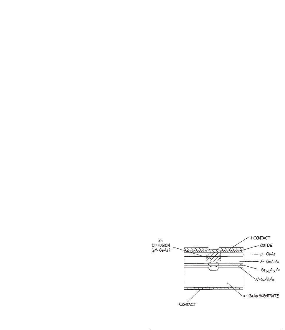
typically 10–20 ns long. Passive Q-switching can also be
accomplished with a ‘‘bleachable’’ dye solution placed in an
optical cell inside the laser cavity. The dye is opaque at low
incident light intensities and inhibits the buildup of laser
oscillation. When, however, the laser acquires enough gain
to overcome the intracavity dye absorption loss, laser oscil-
lation begins, the dye bleaches, and a Q-switched pulse
results. A bleachable dye cell with a short relaxation time,
placed close to one of the laser mirrors, will frequently lead
to mode-locked operation
99–101
within the Q-switched pulse
(see Section 4.6.4).
Semiconductor Lasers. Five principal types of
semiconductor laser are available commercially:
(1) Wide bandgap semiconductor lasers based on GaN/
AlGaN, which, depending on stoichiometry, can emit
down to 375 nm. These UV, blue, and green diode
lasers have power outputs of several milliwatt and
above. The developer of the shortest wavelength laser
diodes based on GaN is Nichia, other manufacturers
include Coherent, Cree, Koheras, Micro Laser Sys-
tems, Sony, and Toptica. Wavelengths above 375 nm
are obtained from diodes with elements such as
indium, aluminum, gallium, or nitrogen added, which
produces laser diodes with wavelengths from 480 to
520 nm. The availability of short wavelength diode
and diode-pumped solid-state lasers has significantly
reduced the market and applications for visible and
UV gas lasers such as argon ion, helium–cadmium,
helium–neon, and krypton ion.
(2) GaAs or GaAlAs lasers, which operate at fixed wave-
lengths in the region between 0.75 and 0.9 lm. These
lasers are very inexpensi v e and reliable; they are widely
used in communication and information-processing sys-
tems, and in compact-disk players. High-po wer versions
are used as the pumping source in DPSS lasers.
(3) InGaAsP lasers operate principally in the 1.3 and
1.55 lm regions for telecommunications applications.
They have been developed to operate at the optimum
wavelengths for minimum dispersion and lowest loss
in optical-fiber communication systems. Near infrared
semiconductor lasers are described in detail in many
specialized texts.
102–110
(4) Tunable diode lasers, which utilize lead-salt semicon-
ductors such as PbSSe, PbSnSe, and PbSnTe can
provide tunable operation over limited regions any-
where between 3 and 30 lm. The tunable lead-salt
diode lasers are now commonly used in high-resolu-
tion spectroscopy.
111
They generally emit several
modes, which, because of the very short length of
the laser cavity, are spaced far enough in wavelength
for a single one to be isolated by a monochromator.
The output laser linewidths that are obtainable in this
way are about 10
–4
/cm
1
(3 MHz). Scanning is accom-
plished by changing the temperature of the cryogeni-
cally cooled semiconductor or the operating current.
Complete tunable-semiconductor-laser spectroscopic
systems are available from Quantum Associates or
Spectra-Physics (Laser Analytics).
(5) Quantum cascade lasers
112
can provide tunable oper-
ation over specific limited spectral regions within a
range from 3 to 211 lm. The wavelength range varies
from manufacturer to manufacturer. These lasers use
multiple quantum wells, a so-called superlattice,to
provide laser operation between sub-bands in the con-
duction bands of the structure. These lasers do not use
p-n junctions for their operation. Quantum cascade
lasers are available from Alpes, Boston Electronics,
Cascade Technologies, and Sacher Lasertechnik.
Semiconductor Laser Properties. Only researchers
involved in semiconductor laser development will fabricate
these lasers. Their laser performance is, however, strongly
influenced by their generally small size, and device
structure. Figures 4.129–4.132 give examples of some
Figure 4.129 Double heterostructure laser diode design
using a stripe excitation region confined by an oxide layer
and deep zinc diffusion.
LASERS 277
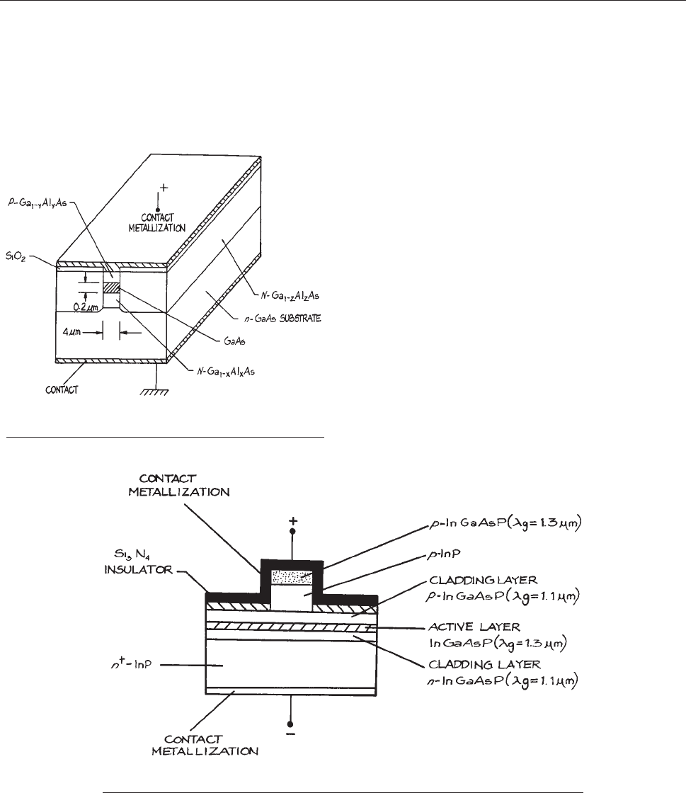
representative structures that are used in current
semiconductor diode lasers. The basic laser structure
involves a p-n junction through which a drive current
flows. In all these structures the current flow through the
device is controlled so that a specific volume of the active
region is excited. This region is generally very small. The
active length is not generally more than 1–2 mm. The
lateral dimensions of the active region are generally in
the 5–10 lm range, however, in single quantum well
(SQW) and multiple quantum well (MQW) lasers, the
dimension of the active region in the direction of current
flow can be as small as 10–100 nm.
Laser oscillation occurs in a resonant Fabry–Perot
structure made up of the two end facets of the laser.
The active region acts like a waveguide to c onfine the
laser beam, which ideally emerges from the emitting
facet as an elliptical Gaussian beam. This is a Gaussian
beam whose spot sizes w
x
, w
y
are different in the two
orthogonal (x, y) directions perpendicular to the z prop-
agation direction of the laser beam. The smaller spot size
is generally in the direction perpendicular to the junc-
tion. This asymmetry of the laser beam causes its beam
divergence to be larger in the direct ion perpendicular to
the jun ction than it is in the orthog onal direction, as
shown schematically in Figure 4.133. Commercial diode
lasers
are often supplied with an anamorphic beam
expander, whic h circularizes the laser beam and equal-
izes its orthogonal beam divergence angles, however, in
general the beam quality from any semiconductor laser is
Figure 4.130 Double heterostructure laser of a buried
stripe design.
Figure 4.131 Cladded ridge double heterostructure semiconductor laser design.
278 OPTICAL SYSTEMS
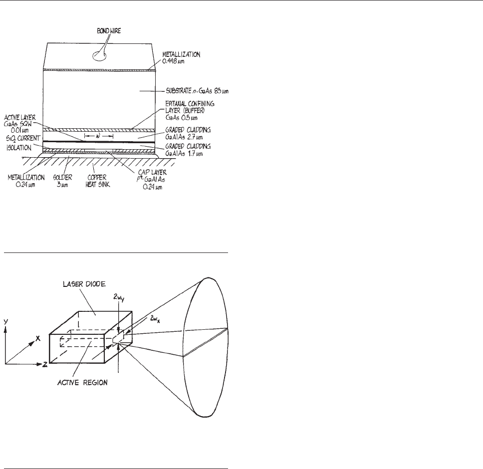
inferior to that from m ost gas lasers. A circular, clean,
output beam ca n be obtain ed from a fiber-coupled diode
laser. Vertical cavity surface emitting lasers (VCSELs)
also provide circular output beams.
The spectral purity of Fabry–Perot semiconductor lasers
is generally inferior to helium–neon lasers or diode-
pumped solid-state lasers. Semiconductor laser linewidths
are typically several MHz or more, so their coherence
lengths are short. This makes them less suitable in most
interferometric applications than most gas lasers or diode-
pumped solid-state (DPSS) lasers. Narrower linewidth
semiconductor lasers use an external cavity incorporating
a grating structure, or have a Bragg grating structure incor-
porated into the semiconductor material itself: so-called
distributed feedback (DFB) or distributed Bragg reflection
(DBR) lasers. Suppliers include Agere, AMS Technolo-
gies, EXFO, Infineon, Lasermate, Sacher Lasertechnik,
and Toptica. These lasers are mostly available at the tele-
communications wavelengths of 1300 nm and 1550 nm.
Diode lasers have achieved their greatest commercial
importance in telecommunications systems, but the avail-
ability of diode lasers at many discrete wavelengths from
375 nm to beyond 2 lm
31
has increased their use in spec-
troscopic applications. They can provide some degree of
tunability by changing their operating temperature or drive
current. Suppliers include Applied Optronics, Coherent,
DILAS, Laser Diode, Lasermate Group, Lasertel, Melles
Griot, New Focus, Newport, Opton, Photonic Products,
Point Source, and QPC Lasers. Manufacturers’ data sheets
should be consulted for wavelengths, mode quality (single
or multimode), beam quality (circular or elliptical),
powers, and operational currents.
31
Many of these lasers
can be obtained coupled to an optical fiber, which provides
a clean, circular beam.
Some of the commonly available wavelengths (in nm)
from diode lasers are: 375, 405, 408, 440, 635, 640, 650,
670, 690, 730, 780, 808, 830, 915, 940, 980, 1300, 1370,
1470, 1550, 1720, 1850, 1907, 1950, 2004, and 2350.
High-power diode lasers are available with powers up to
and beyond 1 kW. They are widely used as pump sources
in diode-pumped solid-state lasers; however, as far as spec-
troscopy purity is concerned they are closer in character to
a light-emitting diode than they are to high-coherence
lasers such as helium–neon, helium–cadmium or diode-
pumped Nd:YAG.
Diode-Pumped CW Solid-State Lasers. Because
of a fortuitous coincidence between the output of GaAlAs
semiconductor lasers working near 809 nm and a strong
absorption of the neodymium ions (Nd
3+
) in YAG, YLF, or
YVO
4
, it is very efficient to optically pump Nd
3+
lasers
Figure 4.133 Schematic diagram of how a semiconductor
laser emits a quasi-elliptical output beam because of
asymmetrical beam confinement in two orthogonal
directions inside the laser structure.
Figure 4.132 Graded index separate confinement
heterostructure (GRINSCH) semiconductor laser design.
Typical dimensions of the various layers are indicated. For a
narrow stripe laser w ~5lm, for a broad stripe laser w ~60
lm.
LASERS 279
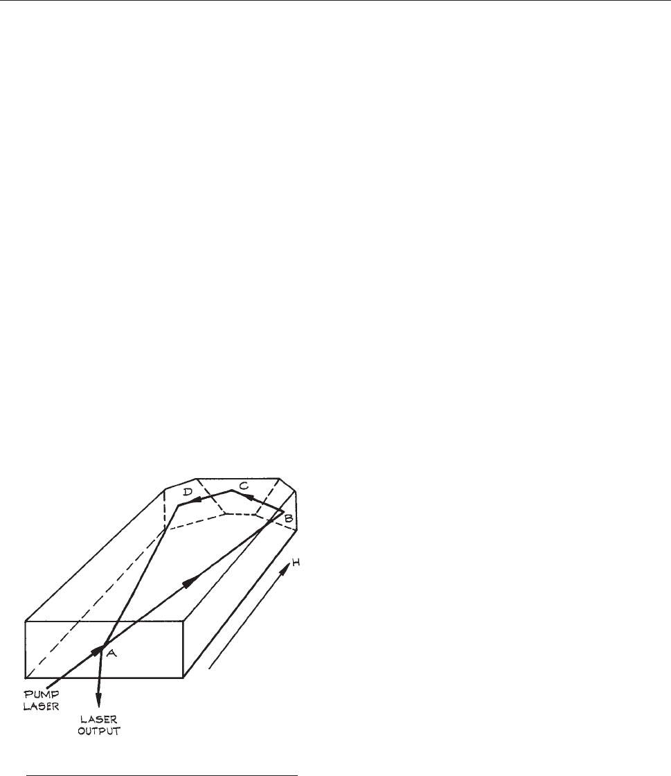
with diode lasers. These lasers have become widely
available commercially. They can also be efficiently
frequency doubled to 530 nm, so have begun to replace
ion lasers in applications where intense green light is
required. Green output powers up to 70 W are available.
Diode-pumped lasers in which the semiconductor lasers
are arranged to inject their pump radiation through the cy-
lindrical faces of a laser rod are in many ways akin to
lamp-pumped lasers of the same kind. Because of the high
electrical efficiency of GaAlAs laser diodes (>10%) the
ov erall electrical-to-optical conversion ef ficienc y of these
lasers is very high, approaching 10%. If the diode laser pump
radiation is injected along the axis and matched to the trans-
verse mode geometry of the solid-state laser then very stable,
narrow linewidth laser oscillation can be obtained: Figure
4.134 shows the clev er monolithic Nd:YA G laser design of
Kane
and Byer .
113
In this laser the magneto-optical proper-
ties of YAG are used to obtain unidirectional amplification of
a trav eling wave in the laser cavity. This prev ents the spatial
hole-burning that can occur in a standing wav e homogene-
ously broadened laser, which can allow multiple longitudinal
modes to oscillate.
15
Frequency doubling of a DPSS laser is generally carried
out with an intracavity nonlinear crystal such as BBO (beta-
BaB
2
O
4
), PPLN (periodically poled lithium niobate), or
PPKTP [periodically poled potassium titanium oxide phos-
phate (KTiOPO
4
)], or with an external resonant cavity
containing a nonlinear crystal. Figure 4.135 shows how
in
tracavity frequency doubling is done with a Nd:YVO
4
coherent Verdi laser. This use of a ring laser resonator with
unidirectional laser oscillation provides single longitudinal
mode operation and a narrow linewidth. Frequency-tripled
operation of diode-pumped Nd
3+
laser at 355 nm is avail-
able at powers in excess of 3 W, frequency-quadrupled oper-
ation at 266 nm provides powers up to 500 mW. There are
many suppliers of diode-pumped Nd
3+
lasers, including A-
B Lasers, Alphalas, Cobolt AB, Coherent, Continuum, Lee
Laser, Lightwave Electronics, Melles Griot, Quantronix,
Spectra-Physics, TecOptics, and TRUMPF, among
others.
31
Diode-pumped solid-state lasers are also avail-
able at other wavelengths, notably 2.1 lm in holmium
(Ho
3+
), 1.6 lm and 2.8 lm in erbium (Er
3+
) and 2.3 lm
in thulium (Tm
3+
).
The principal advantages of this type of laser are reliabl-
ity, narrow linewidth, and single-frequency operation.
Continuous Wave Dye Lasers. Continuous wave
dye lasers usually take the form of a planar jet of dye
solution continuously sprayed at Brewster’s angle from a
slit nozzle, collected, and recirculated. The jet stream is in
a spherical mirror laser cavity, where it is pumped by the
focused radiation of a CW ion laser or frequency-doubled
Nd:YAG laser, as shown in Figure 4.136. These lasers can
generally
be regarded as wavelength converters – they
have essentially the linewidth, frequency, and amplitude
stability of the pumping source. For example, narrow-line-
width operation requires an etalon-controlled single-fre-
quency ion laser. Continuous wave dye lasers are quite
efficient at converting the wavelength of the pump laser;
at pump powers far enough above threshold, the conver-
sion efficiency ranges from 10 to 45%. Laser dyes are
available from Exciton Lambda Physik and Radiant Dyes
Laser Accessories, among others. Dye lasers are rapidly
being replaced, wherever possible, with tunable solid-state
devices. The dyes used photodegrade and liquid spills are
common. The laboratories of most dye-laser users are
stained with the dyes that they use! For further details of
CW-dye-laser operation consult Schafer.
78
Continuous
wave dye lasers are available from Big Sky Laser Technol-
ogies, Coherent, Quantel, and Spectra-Physics.
Figure 4.134 The ’’MISER’’ ring laser design of Kane
and Byer.
280 OPTICAL SYSTEMS
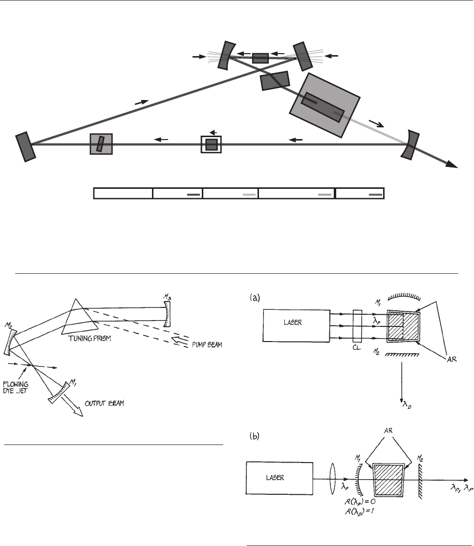
Pulsed Dye Lasers. Continuous wave dye lasers are
not as frequently constructed in the laboratory as are
pulsed dye lasers. In its simplest form, a pulsed dye laser
consists of a small rectangular glass or quartz cell placed
on the axis of an optical resonator and excited with a
focused line image from a pump laser. Two simple
geometrics are shown in Figure 4.137.
+
Temperature-Controlled
Etalon
Optical
Diode
Green
Output
Pump
Pump
HR@1064 nm
AR@632 nm
HR@1064 nm
HT@808 nm
HR@1064 nm
HR3
HR1
Nd:YV0
4
Astigmatic
Compensator
Beam Paths: 808 nm
1064 nm
1064+532 nm
532 nm
Ring Cavity Resonator of Coherent, Inc. Verdi Green DPSS Laser
LBO
OC
Figure 4.135 The layout of the Coherent, Inc. ‘‘Verdi’’ laser where intracavity frequency doubling with a lithium
triborate LiB
3
O
5
(LBO) crystal is used to generate 530 nm from 1.06 lm. The initial laser oscillation is at 1.064 l using a
neodymium-doped yttrium vanadate (Nd:YVO
4
) crystal pumped with an 808 nm diode laser. In the diagram HR – high
reflectance mirror; OC – output coupling mirror.
Figure 4.136 Layout of a CW dye laser using a flowing
dye jet.
Figure 4.137 Two simple pulsed dye laser arrangements:
(a) transverse pumping; (b) longitudinal pumping.
LASERS 281
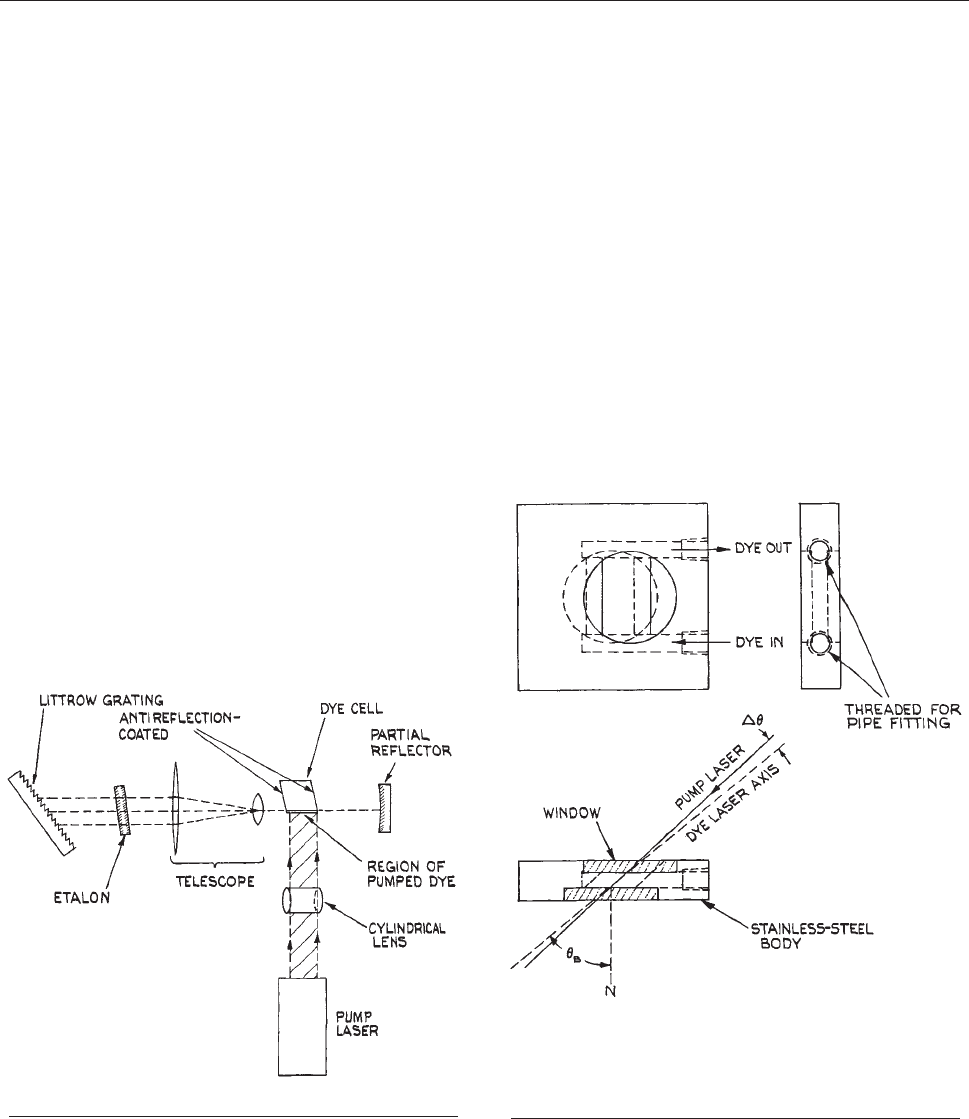
The most commonly used pump lasers are N
2
and
frequency-doubled Nd:YAG, although ruby, excimer and
copper-vapor lasers are also used. In its simplest form, this
type of pulsed dye laser will generate a broad-band laser
output (5–10 nm). Various additional components are
added to the basic design to give tunable, narrow-linewidth
operation. A very popular design that incorporates all the
desirable features of a precision-tunable visible source has
been described by Ha
¨
nsch.
114
The essential components of
aHa
¨
nsch-type pulsed dye laser are shown in Figure 4.138.
The
pump laser is focused, with a cylindrical and/or a
spherical lens, to a line image in the front of a dye cell. The
line of excited dye solution (for example a 5 3 10
–3
molar
solution of Rhodamine 6G in ethanol) is the gain region of
the laser. The laser beam from the gain region is expanded
with a telescope in order to illuminate a large area of a high
dispersion, Littrow-mounted echelle grating. Rotation of
the grating tunes the center wavelength of the laser. With-
out the telescope, only a small portion of the grating is
illuminated, high resolution is not achieved, and the laser
linewidth will not be very narrow. With telescope and
grating alone, the laser linewidth will be on the order of
0.005 nm at 500 nm (’ 0.2 cm
1
). Even narrower linewidth
can be achieved by including a tilted Fabry–Perot etalon
in the cavity. A suitable etalon will have a finesse of 20 and
a free spectral range (see Section 4.7.4) below about 1 cm
1
in this case. Line widths as narrow as 4 3 10
–4
nm can be
achieved. A few experimental points are worthy of note:
the laser is tuned by adjusting grating and/or etalon; align-
ment of the telescope to give a parallel beam at the grating
is quite critical; the dye should be contained in a cell with
slightly skewed faces to prevent spurious oscillation; the
dye solution can remain static when low-power (10–100
kW) pump lasers are used, magnetically stirred when
pump lasers up to about 1 MW are used, or continuously
circulated from a reservoir when higher-energy or high-
repetition-rate pump lasers are used. Suitable dye cells are
available from Anderson Lasers, Esco, Hellma Cells and
NSG Precision Cells. Cells can be constructed from stain-
less steel with Brewster window faces when end-on pump-
ing with a high-energy laser is used (as shown in Figure
4.139). The dye can be magnetically stirred by placing a
small
Teflon-coated stirring button in the bottom of the dye
cell. When continuous circulation of dye is used, suitable
Figure 4.138 Ha
¨
nsch-type pulsed dye laser.
Figure 4.139 Flowing dye cell for end-pumped operation.
N ¼ normal to windows; h
B
¼ Brewster’s angle,
approximately the same for both pump and dye laser
wavelengths; Dh ¼ a small angle. Dye solution flows
laminarly in the channel between the windows.
282 OPTICAL SYSTEMS
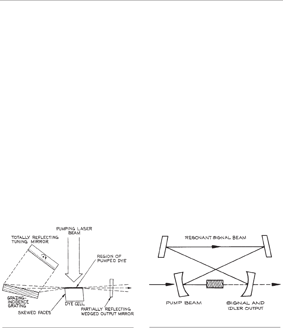
pumps are available from Fluid-o-Tech and Micropump
Corporation.
Once a narrow-linewidth pulsed-dye-laser oscillator has
been constructed, its output power can be boosted by pass-
ing the laser beam through one or more additional dye
cells, which can be pumped with the same laser as the
oscillator. In a practical oscillator-amplifier configuration,
10% of the pump power will be used to drive the oscillator
and 90% to drive the amplifier(s). Further details of
Ha
¨
nsch-type dye-laser construction are available in several
publications.
115–119
Two other approaches to achieving narrow-linewidth
laser oscillation are worthy of note. The intracavity-
telescope beam expander can be replaced, by a multiple-
prism beam expander (see Section 4.3.4), which expands
the
beam onto the grating in one direction only. Such an
arrangement does not need to be focused. An alternative,
simple approach described by Littman
118,119
is to elimi-
nate the beam expander and instead use a Littrow-mounted
holographic grating in grazing incidence, as shown in Fig-
ure
4.140. Linewidths below 0.08 cm can be obtained with-
out
the additional use of an intracavity etalon.
Optical Parametric Oscillators. At one time, opti-
cal parametric oscillators (OPOs) were not readily avail-
able commercially, and were tricky to use. This has
changed. Optical parametric oscillators provide tunable
radiation typically in the range 210–5000 nm. They operate
by using nonlinear optical processes in a crystal.
15,120–124
The OPO requires a pump laser of frequency m
P
,whichis
passed through a nonlinear crystal such as PPLN. Two
new frequencies are generated in this process, a signal of
frequency m
S
, and an idler of frequency m
I
. Energy is con-
served in this process so that m
S
¼ m
P
– m
I
. Tunability results
by changing the angle of the pump beam with respect to the
optic axis of the crystal, or by changing the temperature of
the crystal. One or more of the three frequencies, pump,
signal, or idler, is resonated inside a resonant structure that
surrounds the nonlinear crystal. Figure 4.141 shows a sche-
mat
ic of an OPO with a resonant signal beam. An OPO
generally generates tunable radiation with relatively broad
linewidths (>1 cm). Special techniques are needed to gen-
erate narrow linewidths.
125
Optical parametric oscillators
are available from Coherent, Continuum, EKSPLA, Linos
Photonics, Opotek, Quantel, Radiantis, and Spectra Physics.
Pulsed OPOs are more readily available than CW OPs and
have larger tuning ranges. They can also generate very
short (femtosecond) pulses.
4.6.4 Laser Radiation
Laser radiation is highly monochromatic in most cases,
although flashlamp-pumped dye lasers in a worst case
may have linewidths as large as 100 cm
1
(2.5 nm at 500
nm). The spectral characteristics of the radiation vary from
laser to laser, but will be specified by the manufacturer.
Lasers are usually specified as single-mode lasers or multi-
mode lasers.
Figure 4.140 Littman-type dye laser.
Figure 4.141 Schematic layout of an optical parametric
oscillator (OPO).
LASERS 283

A single-mode laser emits a single-frequency output.
Continuous wave CO
2
lasers and other middle- and far-
infrared lasers usually operate in this way, and helium–
neon and argon–ion lasers can also be caused to do so.
The single output frequency will itself fluctuate randomly,
typically over a bandwidth of 100 kHz–1 MHz, unless
special precautions are taken to stabilize the laser – usually
by stabilizing the spacing between the two mirrors that
constitute its resonant cavity.
Multimode lasers emit several modes, called longitu-
dinal modes, spaced in freq uency by c
0
/2L,wherec
0
is
the velocity of light in vacuo and L is the optical path
length between the re sonator mirrors. In a med ium of
refractive index n and geometric length l, L ¼ nl.There
may, in fact, be several superposed combs of equally
spaced modes in the output of a multimode laser if it
is not operating in a single transverse mode. The trans-
verse modes specify the different spatial distributions of
intensity that are possible in the output beam. The most
desirable such mode, which is standard in most goo d
commercial lasers, is the fundamental TEM
00
mode,
which has a Gaussian radial intensity distribution (see
Section 4.2.4). A laser will generally operate on multi-
ple
longitudinal modes if the linewidth Dv of the ampli-
fying transition is much greater than c
0
/2L. In this case,
the output frequencies will spa n a frequency r ange o n
the order of Dv. In short-pulse lasers the radiation oscil-
lating in the laser cavity may not be able to make many
passes during the duration of the laser pulse, and (par-
ticularly if the linewidth of the amplifying transition is
very large) the individual modes may not have time to
become well characterized in frequency. T his is the sit-
uation that prevails in pulsed dye and excimer lasers.
Additional frequency-selective components must be
included in such lasers, such as etalons and/or diffrac-
tion gratings, to obtain narrow output linewidths.
Laser radiation is highly collimated: beam divergence
angles as small as 1 mrad are quite common. This makes a
laser the ideal way to align an optical system, far superior
to traditional methods using point sources and autocolli-
mators. As mentioned previously, lasers are highly coherent.
Single-mode lasers have the highest temporal coherence –
with coherence lengths that can extend to hundreds of
kilometers. Fundamental-transverse-mode lasers have the
highest spatial coherence.
In multimode lasers, the many output frequencies lie
underneath the gain profile, as s hown in Figure 4.12 1.
Laser
oscillation can be restricted to a single transverse
mode by appropriate choice of mirror radii and spacing.
Then, the available output frequencies are uniformly
spaced longitudinal modes a frequency c
0
/2L apart,
where L is the optical spacing of the laser mirrors. Laser
oscillation can be restricted to a single one of these
longitudinal modes by placing an etalon inside the laser
cavity. The etalon should be of such a length l that its
free spectral range c/2l is greater than the width of the
gain profile, Dv. Its finesse should be high enough so
that c/2lF < c
0
/2L. The etalon acts as a filter that allows
only one longitudinal mode to pass without incurring
high loss.
Many lasers ca n be operated in a mode -locked fash-
ion. Then the longitudinal modes of the laser cavity
become locked together in phase and the output of the
laser becomes a train of uniformly spaced, very narrow
pulses. The spacing between these pulses corresponds to
the round-trip time in the laser cavity, c
0
/2L.Thetem-
poral width of the p ulses is inversely proportional to the
gain band width; th us, the broader the gain profile, the
narrower the o utput pulses in m ode-locked operation .
For example, an argon-ion laser with a gain profile 5
GHz wide can yield mode-locked pulses 200 lswide.
A mode-locked dye laser with a linewidth of 100 cm
(3 3 10
12
Hz) can, in principle, give mode-locked pulses
as short as about 0. 3 ps.
Even shorter pulses than this can be obtained with ring-
dye lasers, with mode-locked Ti:sapphire lasers, or with
colliding pulse mode-locking techniques,
15
which, with
pulse compression techniques, can generate pulses a few
tens of femtoseconds (10
–15
s) long. Ultrafast laser systems
are available from Big Sky Laxer, Clark-MXR, Coherent,
Quantronix, and Spectra Physics (now Newport).
Pulse compressors are available from Calmar Optcom,
Femtochrome Research, and Swamp Optics.
4.6.5 Coupling Light from a Source to
an Aperture
A common problem in optical experiment design involves
either the delivery of light from a source to a target, or
284 OPTICAL SYSTEMS
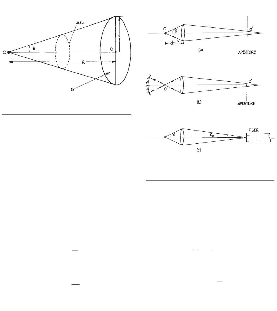
collection of light from a source and delivery of the light to
a collection aperture. The collection aperture might be the
active area of a photodetector, the entrance slit of a spec-
trometer, or the facet of an optical fiber. A problem of
specific importance is the focusing of a laser beam to a
small spot. Sometimes the solution to one of these prob-
lems will involve a imaging system, but it might also
involve a nonimaging light collector.
(1) Collection of light from a point source and its delivery
to a target aperture. This situation is illustrated in
Figure 4.142. The solid angle DX sub
tended by a cir-
cular aperture S ¼ pa
2
at distance R from the source is:
DX ¼ 2pð1 cos hÞð4:220Þ
which for R >> a can be written as:
DX ¼
S
R
2
ð4:221Þ
If the radiant power of the source is P watts then the
power, collected by the aperture is:
P
0
¼ P
DX
4p
ð4:222Þ
To increase the light delivered to the aperture S, a lens
system can be placed between O and O9 as shown in
Figure 4.143. To maximize light collection, the lens
used
should have a small f/number (f/#). The point
source is placed close to the focal point of the lens,
so that:
cos h ’ f =
ffiffiffiffiffiffiffiffiffiffiffiffiffiffiffiffi
a
2
þ f
2
q
ð4:223Þ
and
P
0
¼
P
2
1
f
ffiffiffiffiffiffiffiffiffiffiffiffiffiffiffiffi
a
2
þ f
2
p
!
ð4:224Þ
Since the f/number is:
f =# ¼
f
2a
ð4:225Þ
Equation (4.224) becomes:
P
0
¼ P
1
2
f =#
ffiffiffiffiffiffiffiffiffiffiffiffiffiffiffiffiffiffiffiffiffi
1 þ 4f =#
p
!
ð4:226Þ
Figure 4.143 Optical arrangements for optimizing cou-
pling of a point source to an aperture: (a) lens coupling; (b)
lens and spherical mirror coupling; (c) coupling of a point
source to an optical fiber.
Figure 4.142 Geometry used to determine the collection
efficiency of an aperture when it is illuminated by light from
a point source.
LASERS 285
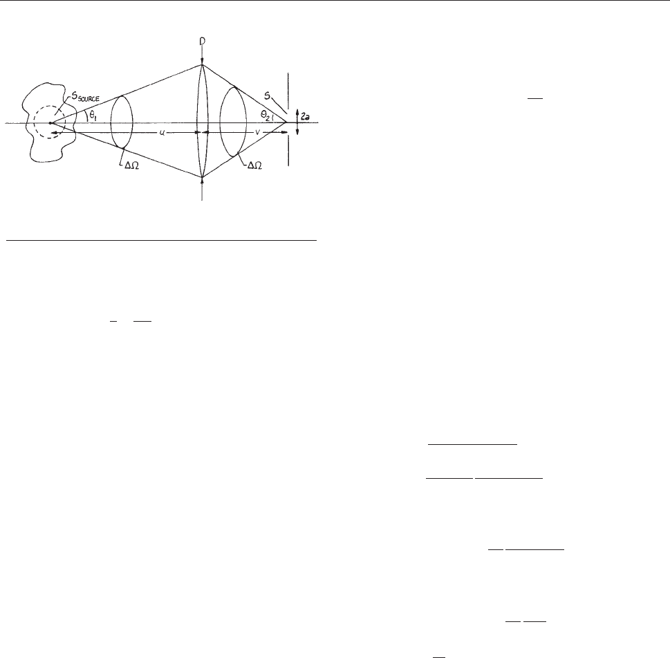
With an f/1 lens
P
0
¼ P
1
2
1
ffiffiffi
5
p
¼ 0:053P ð4:227Þ
In practice an aspheric lens should be used in this
application, especially if the aperture S is of small size.
If a spherical reflector is placed behind the source, as
shown in Figure 4.143(b), so that the source lies at its
center
of curvature, then the collection efficiency can
be doubled.
(2) Coupling light from a point source to an optical fiber.
Whether the source is actually a point source or is of
small finite size relative to other distances in the geo-
metry of Figure 4.143(c) is not very important. For
coupling
light to a fiber, the source must be imaged
onto the front end of the cleaved fiber, but the light
rays must remain within the numerical aperture of the
fiber: sin h
0
< NA. In principle, this can be accom-
plished by placing the source close to the focal point of
the lens so that linear magnification (v/u) is large. In
practice, the maximum magnification that can be used
will be limited by the core diameter of the fiber and the
finite size of the source.
(3) Collection of light from an extended source and its
delivery to a aperture. This situation is shown in
Figure 4.144. It is not possible in this case to image
t
heextendedsourcetoapoint,thebestthatcanbe
done is to image as large an area of the source as
possible onto the aperture S. If an axial point on the
source is imaged to t he center of the aperture S,then
the a rea of the source that can be imaged onto the
aperture S is
S
source
¼
S
m
2
ð4:228Þ
since m ¼ (v/u) is the linear magnification of the sys-
tem. A high-quality imaging system would need to be
used in this situation, especially if the aperture S is
small, otherwise, aberrations will affect the size of
the image.
If the brightness of the extended source in Figure 4.144
is B
1
(Wm
2
sr
1
), then the power collected by the lens
is, approximately:
P
1
¼ 2pB
1
S
source
ð1 cos h
1
Þð4:229Þ
This light is imaged onto the collection aperture of
area S where it occupies a solid angle DX
2
determined
by the angle h
2
, where:
DX
2
¼ 2pð1 cos h
2
Þð4:230Þ
The brightness of the image is:
B
2
¼
P
1
2pSð1 cos h
2
Þ
¼
B
1
S
source
S
ð1 cos h
1
Þ
ð1 cos h
2
Þ
ð4:231Þ
which gives:
B
2
¼
B
1
m
2
sin
2
ðh
1
=2Þ
sin
2
ðh
2
=2Þ
ð4:232Þ
For a paraxial system sinðh
1
=2Þ’ðh
1
=2Þ, so:
B
2
¼
B
1
m
2
ðh
2
1
Þ
ðh
2
2
Þ
ð4:233Þ
The ratio
h
2
h
1
is the angular magnification, m9, of the
system. Therefore, since mm9 ¼ 1:
B
2
¼ B
1
ð4:234Þ
This is an example of the brightness theorem, which
states that the brightness of an image can not be greater
than the brightness of the object.
k
Figure 4.144 Geometry of an extended source and
collection aperture used to describe the collection efficiency.
286 OPTICAL SYSTEMS

4.6.6 Optical Modulators
In many optical experiments, particularly those involving
the detection of weak light signals or weak electrical sig-
nals generated by some light-stimulated phenomenon, the
signal-to-noise ratio can be considerably improved by the
use of phase-sensitive detection. The principles underlying
this technique are discussed in Section 6.8.2. To modulate
the
intensity of a weak light signal falling on a detector, the
signal must be periodically interrupted. This is most easily
done with a mechanical chopper. Weak electrical signals
that result from optical stimulation of some phenomenon
can also be modulated in this way by chopping the radia-
tion from the stimulating source.
Modulation of narrow beams of light such as laser
beams, or of extended sources that can be focused onto a
small aperture with a lens, is easily accomplished with a
tuning-fork chopper. Such devices are available from
Boston Electronics, Electro-Optical Products, and Scitec
Instruments. The region chopped can range up to several
millimeters wide and a few centimeters long at frequencies
from 5 Hz to 3 kHz. For chopping emission from extended
sources, or over large apertures, rotating chopping wheels
are very convenient. The chopping wheel can be made of
any suitable rigid, opaque material and should have radi-
ally cut apertures of one of the forms indicated in Figure
4.145. This form of aperture ensures that the mark-to-space
ratio
of the modulated intensity is independent of where the
light passes through the wheels. By cutting very many slots
in the wheel, very high modulation rates can be achieved –
for example, up to 100 kHz with a 20 000 rpm motor and a
wheel with 300 slots. The chopping wheel should usually
be painted or anodized matt black. For chopping intense
laser beams (in excess of perhaps 1 W), it may be better to
make the wheel reflective so that unwanted beam energy
can be reflected into a beam dump. Reflective glass chop-
ping wheels can be used at low speeds in experiments
where a light beam must be periodically routed along
two different paths.
To obtain an electrical reference signal that is synchro-
nous with a mechanical chopping wheel, a small portion
of the transmitted beam, if the latter is intense enough, can
be reflected onto a photodiode or phototransistor. Alterna-
tively, an auxiliary tungsten filament lamp and photodiode
can be mounted on opposite sides of the wheel. If these are
mounted on a rotatable arm, the phase of the reference
signal they provide can be adjusted mechanically. Chop-
ping wheels with built-in speed control and electrical rota-
tion reference signals are available commercially from
Boston Electronics, DL Instrument, EG&G Princeton
Applied Research, Electro-Optical Products Corp., New
Focus, Stanford Research Systems, and Thorlabs.
Electro-optic modulators (Pockel’s cells) can also be
used in special circumstances, particularly for modulating
laser beams, or when mechanical vibration is undesirable.
The operation of these devices is shown schematically in
Figure 4.146. Light passing through the electro-optic crys-
tal
is plane-polarized before entry and then has its state of
polarization altered by an amount that depends on the
voltage applied to the crystal. The effect is to modulate
the intensity of the light transmitted through a second lin-
ear polarizer placed behind the electro-optic crystal. By
choosing the correct orientation of the input polarizer rela-
tive to the axes of the electro-optic crystal and omitting
the output polarizer, the device becomes an optical phase
modulator. For further details of these electro-optic ampli-
tude and phase modulators the reader is referred to the
books by Yariv,
14
Kaminow,
125
and Davis.
15
Electro-optic
modulators are available from Cleveland Crystals, Conop-
tics, II-VI, JDS Uniphase, Meadowlark Optics, New Focus,
and Quantum Technology, among others.
Acousto-optic modulators which operate by diffraction
effects induced by sound-wave-produced periodic density
variations in a crystal are also available.
126,127
The most
widely used materials for these devices are LiNbO
3
,TeO
2
,
and fused quartz. In their operation a radio-frequency (r.f.)
sound wave is driven through the material from a piezo-
electric transducer, usually fabricated from LiNbO
3
or
ZnO. A schematic diagram of how such an acousto-optic
modulator works is given in Figure 4.147. Incident light
Figure 4.145 Some chopping-wheel designs.
LASERS 287
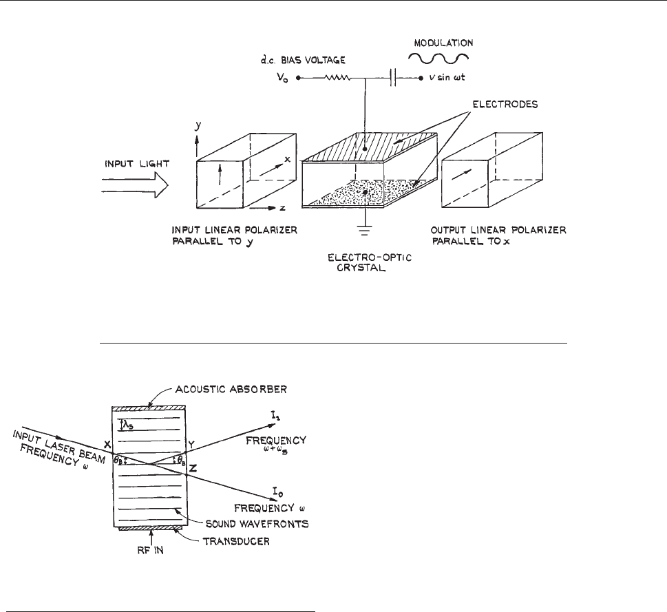
that makes an appropriate angle h
B
, with the sound wave-
fronts will be diffracted if it simultaneously satisfies the
condition for constructive interference and reflection from
the sound wavefronts. This condition is sin h
B
¼ k/k
s
,
where k is the laser wavelength in the acousto-optic mate-
rial, and k
s
is the sound wavelength. The device is used as
an amplitude modulator by amplitude-modulating the
input r.f., which will be set to a specific optimum fre-
quency for the device being used. Increase of drive power
increases the diffracted power I
1
and reduces the power of
the undeviated beam I
0
and vice versa. The device also
functions as a frequency shifter. In Figure 4.147 the laser
beam
reflects off a moving sound wave and is Doppler
shifted so that the beam I
1
is at frequency x þ x
s
, where
x
s
is the frequency of the sound wave. Acousto-optic devi-
ces are available from many suppliers, including Crystal
Technology, Electro-Optical Products, IntraAction, Iso-
met, and NEOS Technologies. Further details about these
devices can be found in References 15, 126, and 127.
Very many liquids become optically active on applica-
tion of an electric field; that is, they rotate the plane of
polarization of a linearly polarized beam passing through
them. This phenomena is the basis of the Kerr cell, which
can be used as a modulator, but is more commonly used as
an optical shutter (for example, in laser Q-switching appli-
cations as discussed in Section 4.6.3). A typical Kerr cell
uses
nitrobenzene placed between two plane electrodes
across which a high voltage is applied. This voltage is
typically several kilovolts and is sufficient to rotate the
plane of polarization of the incident light passing between
the plates by 45 or 90°. Kerr cells are rarely used these days
and have been superseded by electro-optic modulators.
Figure 4.147 Schematic diagram showing the operation of
an acousto-optic device in the Bragg regime. For simplicity,
the refraction of the laser beam at X, Y,andZ is not shown.
Figure 4.146 An electro-optic amplitude modulator using a transversely operated
electro-optic crystal. The d.c. bias voltage can be used to adjust the operating point
of the modulator so that, in the absence of modulation, the output intensity is a
maximum, a minimum, or some intermediate value.
288 OPTICAL SYSTEMS

Closely related to optical modulators are optical deflec-
tors, which can be used for the spatial scanning or switch-
ing of light beams. Two principal types are commonly
used: electromechanical devices that utilize small mirrors
mounted on galvanometer suspensions (available from
Cambridge Technology, GSI Lumonics, and NEOS Tech-
nologies) and beam deflectors that utilize the acousto-optic
effect. In the latter the deflection angle shown in Figure
4.147 is controlled by changing the r.f. drive frequency.
These
devices are available from Crystal Technology,
IntraAction, Isomet, and NEOS Technologies. Electro-
optic scanners are also available, but are less widely used.
These devices are generally designed for small deflections.
They are available from Conoptics.
Spatial light modulators are multiple element devices,
which generally use liquid crystals, work in transmission,
and can modify the characteristics of an entire wavefront in
a pixellated fashion. They are available from Display Tech
and Meadowlark Optics.
4.6.7 How to Work Safely with
Light Sources
Light sources, whether coherent or incoherent, can present
several potential safety hazards in the laboratory. The pri-
mary hazard associated with the use of home-built optical
sources is usually their power supply. Lasers and flash-
lamps in particular, generally operate with potentially
lethal high voltages, and the usual safety considerations
for constructing and operating such power supplies should
be followed in their design:
(1) Provide a good ground connection to the power supply
and light-source housing.
(2) Screen all areas where high voltages are present.
(3) Install a clearly visible indicator that shows when the
power supply is activated.
(4) HV power supplies, particularly those that operate
with pulsed power, can remain dangerous even after
the power is turned off, unless energy-storage capaci-
tors are automatically shunted to ground. Always short
the capacitors in such a unit to ground after the power
supply is turned off before working on the unit.
(5) As a rule of thumb, keep a gap of about 25 mm for
every 10 kV between high-voltage points and ground.
(6) To avoid excessive corona at voltages above about 20
kV, make sure that high-voltage components and con-
nections have no sharp edges. Where such points must
be exposed, corona can be reduced by installing a spher-
ical metal corona cap on exposed items such as bolts or
capacitor terminals. Resistor and diode stacks can be
potted in epoxy or silicone rubber to prevent corona.
(7) Sources that are powered inductively or capacitively
with r.f. or microwave power can burn fingers that
come too close to the power source, even without
making contact.
Commercial optical sources are generally fairly safe
electrically and are likely to be equipped with safety fea-
tures, such as interlocks, which the experimentalist may
not bother to incorporate into home-built equipment. Cav-
eat emptor. Remember the maxim ‘‘it’s the volts that jolts
but it’s the mills that kills.’’
Other general precautions with regard to electric shock
include the following:
(1) Avoid wearing metallic objects such as watches,
watchbands, and rings.
(2) If any operations must be performed on a line circuit,
wear well-insulated shoes and, if possible, use only
one hand – ‘‘Always keep one hand in your pocket.’’
(3) Keep hands dry; do not handle electrical equipment if
you are sweating.
(4) Learn rescue and resuscitation procedures for victims
of electric shock: Turn off the equipment, remove the
victim by using insulated material; if the victim is not
breathing, start mouth-to-mouth resuscitation; if there
is no pulse, begin CPR procedures immediately; sum-
mon medical assistance; continue resuscitation proce-
dures until relieved by a physician. If the victim is
conscious, but continues to show symptoms of shock,
keep the person warm. Always call for professional
help. (Dial 911 in the USA.)
Other hazards in the use of light sources include the
possibility of eye damage, direct burning (particularly, by
exposure to the beam from a high-average-power laser), and
the production of toxic fumes. The last is most important in
the use of high-power CW arc lamps, which can generate
substantial amounts of ozone. The lamp housing should be
suitably ventilated and the ozone discharged into a fume
LASERS 289

hood or into the open air. Some lasers operate using a
supply of toxic gas, such as hydrogen fluoride and the hal-
ogens. Workers operating such systems must be sufficiently
experienced to work safely with these materials. The Math-
eson Gas Data Book, published by Matheson Gas Products,
is a comprehensive guide to laboratory gases, detailing the
potential hazards and handling methods appropriate to each.
The potential eye hazard presented by most incoherent
sources is not great. If a source appears very bright, one
should not look at it, just as one should not look directly at
the Sun. Do not look at sources that emit substantial ultra-
violet radiation; at the least, severe eye irritation will result –
imagine having your eyes full of sand particles for several
days! Long-term exposure to UV radiation should be kept
below 0.5 lW/cm
2
. Ordinary eyeglasses will protect the
eyes from ultraviolet exposure to some extent, but plastic
goggles that wrap around the sides are better. Colored
plastic or glass provides better protection than clear mate-
rial. The manufacturer’s specification of ultraviolet trans-
mission should be checked, since radiation below 320 nm
must be excluded from the cornea.
The use of lasers in the laboratory presents an optical
hazard of a different order. Because a laser beam is gen-
erally highly collimated and at least partially coherent, if
the beam from a visible or near-infrared laser enters the
pupil of the eye it will be focused to a very small spot on
the retina (unless the observer is very short-sighted). If this
focused spot happens to be on the optic nerve, total blind-
ness may result: if it falls elsewhere on the retina, an extra
blind spot may be generated. Although the constant motion
of the human eye tends to prevent the focused spot from
remaining at a particular point on the retina for very long,
always obey the following universal rule: Never look down
any laser beam either directly or by specular reflection.In
practice, laser beams below 1 mW CW are probably not an
eye hazard, but they should still be treated with respect. A
beam must be below about 10 lW before most workers
would regard it as really safe.
The safe exposure level for CW laser radiation depends
on the exposure time. For pulsed lasers, however, it is the
maximum energy that can enter the eye without causing
damage that is the important parameter. In the spectral
region between 380 and 1.5 lm, where the interior mate-
rial of the eye is transparent, the maximum safe dose is on
the order of 10
–7
J/cm
2
for Q-switched lasers and about
10
–6
J/cm
2
for non-Q-switched lasers. If any potential for
eye exposure to a laser beam or its direct or diffuse reflec-
tion exists, it is advisable to carry out the experiment in a
lighted laboratory: in a darkened laboratory, the fully dark-
adapted human eye with a pupil area of about 0.5 cm
2
presents a much larger target for accidental exposure.
The Laser Institute of America publishes a guide that
shows the maximum permitted exposure in terms of power
and direction for a range of laser wavelengths.
128
Infrared laser beams be yond about 1.5 lm are not a retinal
hazard, as they will not penetrate to the retina. Beams
between1.5and3lm penetrate the interior of the eye to
some degree. Because its energy is absorbed in a distributed
fashion in the interior of the eye, 1.55 lm is one of the safest
laser waveleng ths. Lasers beyond 3 lm are a burn hazard,
and eye exposure must be avoided for this reason. CO
2
lasers,
for example, which operate in the 10 lm region, are less
hazardous than equivalent-intensity argon-ion or neodymium
lasers. Neodymium lasers represent a particularly sev ere haz-
ard: they are widely used, emit substantial po wers and ener-
gies, and operate at the invisible wavelen gth of 1.06 lm. This
wavelength easily penetrates to the retina, and the careless
worker can suffer sev ere eye damage without any warning.
The use of safety goggles is strongly recommended when
using such lasers. These goggles absorb or reflect 1.06 lm,
but allow normal transmission in at least part of the visible
spectrum. Laser safety goggles are available commercially
from several sources, such as Bolle
´
, Control Optics, Glen-
dale, K entek, Lase-R Shield, Melles Griot, Newport, NOIR,
Thorlabs, and UVEX. The purchaser must usually specify
the laser wav elen gth(s) for which the goggles are to be used.
Unfortunately, one problem with goggles prevents their
universal use. Because the goggles prevent the laser wave-
length from reaching the eyes, they prevent the alignment
of a visible laser beam through an experiment by observa-
tion of diffuse reflection of the beam from components in
the system. When such a procedure must be carried out, we
recommend caution and the operation of the laser at its
lowest practical power level during alignment. Frequently,
a weak, subsidiary alignment laser can be used to check the
potential path of a high-power beam before this is turned
on – a strongly recommended procedure. For infrared laser
beams, thermal sensor cards are available that will reveal
the location of an infrared laser beam through thermally
activated fluorescence or fluorescence quenching. They are
290 OPTICAL SYSTEMS

available from Applied Scintillation Technology, Laser
S.O.S., Macken Instruments, Newport, and Solar TII.
Some of these sensor cards or plates, especially for
CO
2
laser beam location, require illumination with a
UV source. Where an infrared laser beam strikes the illu-
minated surface a dark spot appears. Used Polaroid film
and thermally sensitive duplicating paper are also useful
for infrared-beam tracking.
The beam from an ultraviolet laser can generally be
tracked with white paper, which fluoresces where the beam
strikes it. A potential burn and fire hazard exists for lasers
with power levels above about 1 W/cm
2
, although the fire
hazard will depend on the target. Black paper burns most
easily. Very intense beams can be safely dumped onto
pieces of firebrick. Pulsed lasers will burn at output ener-
gies above about 1 J/cm
2
.
In the United States, commercial lasers are assigned a
rating by the FDA Center for Devices and Radiological
Health, which identifies their type, power output range,
and potential hazard. It must be stressed, however, that
lasers are easy to use safely: accidents of any sort have been
rare. Their increasing use in laboratories requires that work-
ers be well-informed of the standard safety practices. For
further discussion of this and all aspects of laser safety and
related topics, we recommend both the book by Sliney and
Wolbarsht
129
and a series of articles on laser safety in the
CRC Handbook of Laser Science and Technology,Vol.1.
130
4.7 OPTICAL DISPERSING
INSTRUMENTS
Optical dispersing instruments allow the spectral analysis
of optical radiation or the extraction of radiation in a nar-
row spectral band from some broader spectral region.
In this general category we include interference filters,
prism and grating monochromators, spectrographs and
spectrophotometers, and interferometers. Interferometers
have additional uses over and above direct spectral
analysis – including studies of the phase variation over an
optical wavefront, which allow the optical quality of opti-
cal components to be measured. Spectrometers, or mono-
chromators as they are generally called, are optical filters of
tunable center wavelength and bandwidth. The output nar-
row-band radiation from these devices is generally detected
by a photon or thermal detector, which generates an elec-
trical signal output. Spectrographs, on the other hand,
record the entire spectral content of an extended bandwidth
region either photographically, or more commonly these
days with a linear detector area. Spectrophotometers are
complete commercial instruments, which generally incor-
porate a source or sources, a dispersing system (which may
involve interchangeable prisms and/or gratings), and a
detector. They are designed for recording ultraviolet, visi-
ble, or infrared absorption and emission spectra.
Spectrofluometers are instruments to record fluorescence
spectra. In such an application two principal modes of spec-
tral usage exist. The emission fluorescence spectrum is the
spectral distribution of emission produced by a particular
monochromatic excitation wavelength. The excitation
spectrum is the total fluorescence emission recorded as
the wavelength of the excitation source is scanned.
Before giving a discussion of important design consider-
ations in the construction of various spectrometers and inter-
ferometers, it is worthwhile mentioning two important
figures of merit that allow the evaluation and comparison
of the performance of different types of optical dispersing
instruments. The first is the resolving power , (<¼k/Dk,
which has already been discussed in connection with diffrac-
tion gratings (Section 4.3.5). The second is the luminosity,
which
is the flux collected by a detector at the output of a
spectrometer when the source at the input has a radiance
of unity. The interrelation between resolving power and
luminosity for spectrometers using prisms, gratings, and
Fabry–Perot etalons has been dealt with in detail by Jacqui-
not.
131
Prism spectrometers have almost disappeared from use
in recent years, however, because of their simple mode of
operation they serve as an archetype in discussing spec-
trometer performance.
Figure 4.148, which shows the essential components of
a
prism monochromator, will serve to illustrate the points
made here. High resolution is clearly obtained in this
arrangement by using narrow entrance and exit slits. The
maximum light throughput of the spectrometer results
when the respective angular widths W
1
, W
2
of the input
and output slits h
1
, h
2
satisfy:
W
1
¼ W
2
ð4:235Þ
OPTICAL DISPERSING INSTRUMENTS 291

where
W
1
¼
h
1
ðda=dkÞ
d
, W
2
¼
h
2
ðdd=dkÞ
a
ð4:236Þ
The angles a are the same as those used in Figure 4.47.
The
input and output dispersions (da/dk)
d
and (dd/dk)
a
are
only equal in a position of minimum deviation, or with a
prism (or grating) used in a Littrow arrangement. If dif-
fraction at the slits is negligible, the intensity distribution
at the output slit when a monochromatic input is used is a
triangular function, as shown in Figure 4.149, where W is
the
spectral width of the slits given by:
W ¼ W
1
¼ W
2
ð4:237Þ
The limit of resolution of the monochromator is:
dk ¼ W ¼
h
2
ðdd=dkÞ
a
ð4:238Þ
The maximum flux passing through the output slit is:
U ¼ TE
e
ðkÞSlh
2
=f
2
ð4:239Þ
where S is the normal area of the output beam, T is the
transmittance of the prism (or efficiency of the grating in
the order used) at the wavelength being considered, l is the
height of the entrance and exit slits (equal), and E
e
(k) is the
radiance of the monochromatic source of wavelength k
illuminating the entrance slit. lh
2
/f
2
is the solid angle that
the exit slit subtends at the output focusing lens. Equation
(4.239) can be written as:
U ¼
TE
e
ðkÞSlkðdd=dkÞ
a
f
2
<
ð4:240Þ
which clearly shows that the output flux is inversely pro-
portional to the resolving power [for a continuous source at
the entrance slit, Equation (4.240) is multiplied by an addi-
tional
factor k/<]. The efficiency E of the monochromator
is defined by the equation:
E ¼
TSl
f
dd
dk
a
ð4:241Þ
where we have assumed the usual case in which
f
1
¼ f
2
¼ f.
To collect all the light from the collimating optics in
the arrangement of Figure 4.148 , the prism or g rating
should
have a normal area at least as large as the aperture
of the collimating optics. Thus, the height of the prism
(or diffraction grating) should be h > W. The ratio f/W,
which is a measure of the light-gathering power of the
monochromator, defines its f/number. The most efficient
way to use a spectrometer of any kind is to send the input
radiation into the entrance slit within the cone of angles
defined by the f/number. The maximum resolution is
obtained if the input f/number matches the spectrometer
f/number. If radiation enters the spectrometer with an f /
number that is too small, this radiation overfills the dis-
persing element and some is wasted. This can be
Figure 4.149 Intensity distribution at the output slit of a
monochromator whose entrance and exit slits have the
same spectral width W.
Figure 4.148 Basic elements of a prism monochromator.
292 OPTICAL SYSTEMS
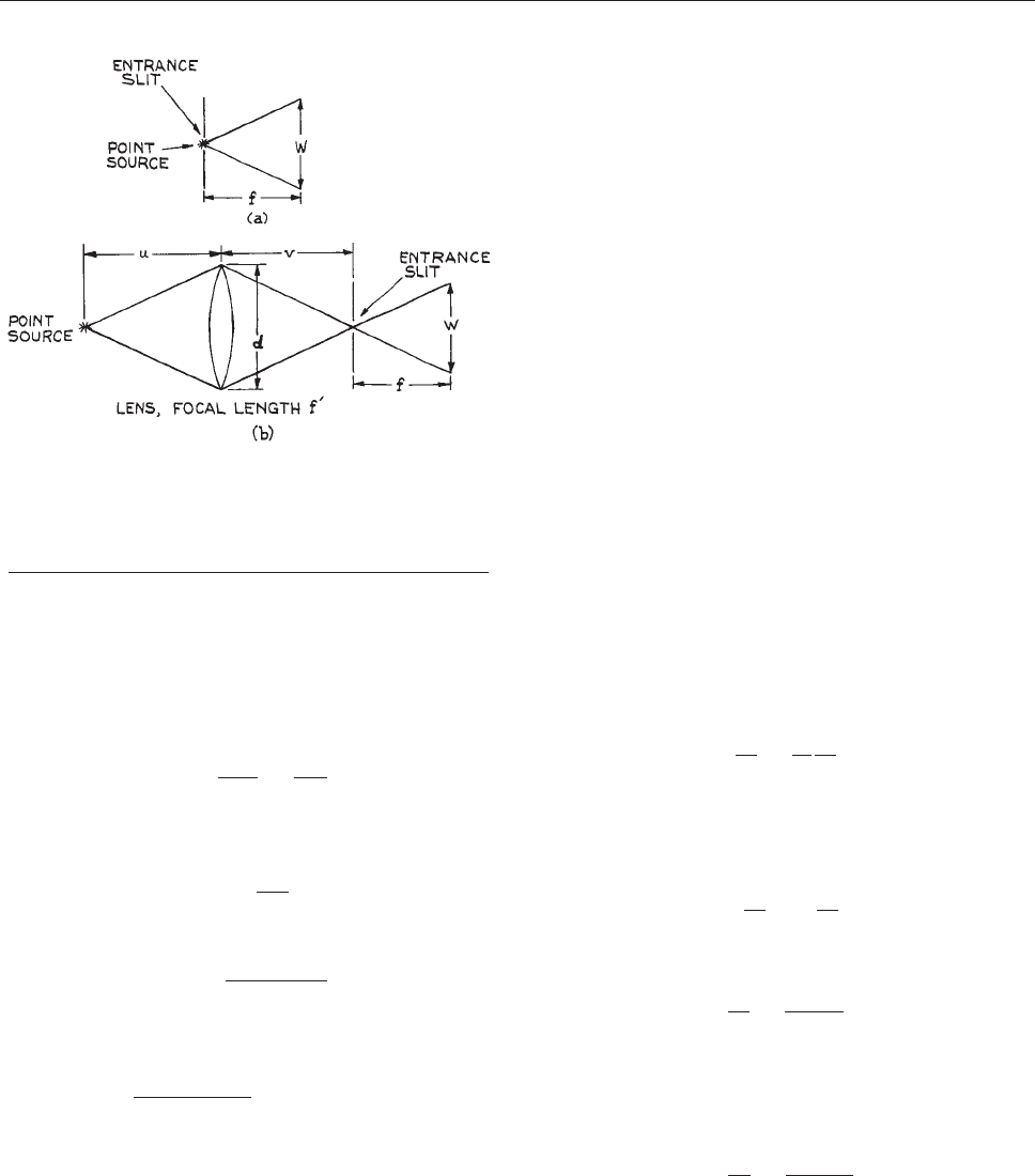
illustrated with the aid of Figure 4.150 , which sh ows t he
use of a point source directly at the entrance slit. In
Figure 4.150(b) a point source is imaged on the en trance
sli
t using a lens that matches the input radiation to the f/
number of the spectrometer. In Figure 4.150(a) the frac-
tional
useful light collection from the source is:
/
1
’
pW
2
4f
2
¼
p
4F
2
ð4:242Þ
where F is the f/number of the spectrometer. In contrast, in
Figure 4.150(b) it is approximately:
/
2
’
pd
2
4u
2
ð4:243Þ
which can be written as:
/
2
¼
pd
2
ðv f Þ
2
4f
2
v
2
ð4:244Þ
and substituting v/d ¼ F, f/d ¼ F9 (the f/number of the
lens), we have:
/
2
¼
pðF=F
0
1Þ
2
4F
2
ðF
0
< FÞð4:245Þ
Thus, equally efficient light gathering to that which would
be obtained with the point source at the entrance slit
results if:
F
0
¼ F=2 ð4:246Þ
More ef ficient light gathering results if F9 is less than this
valu e, but , if the lens and point source are incorrec tly posi-
tioned so that v/d < F, then not all the light collected by the
lens reaches the dispersing element of the spectrometer.
It is quite common for spectrometers to be used with a
fiber optic light-delivery system. If the NA of the fiber is
too large and the fiber optic is placed at the entrance of the
spectrometer, then overfilling of the dispersing element
will occur. In this case correction optics must be included
to match the fiber to the f/number of the spectrometer.
4.7.1 Comparison of Prism and
Grating Spectrometers
Following Jacquinot,
131
we use Equation (4.240) to com-
pare prism and grating instruments. Assume identical val-
ues of l and f
2
, since, for a given degree of aberration of the
system, their values are identical for prisms and gratings.
Blazed-grating efficiencies can be high, so T is assumed to
be similar for prism and grating. Thus, the comparison of
luminosity under given operating conditions of wavelength
and resolution depends solely on the quantity S(dd/dk)
a
for
a prism and S(db/dk)
a
for a grating.
For the prism:
dd
dk
¼
t
W
dn
dk
ð4:247Þ
where, for maximum dispersion, the whole prism face is
illuminated, so that t is the width of the prism base. S ¼ hW
and th ¼ A, the area of the prism base, and so:
S
dd
dk
¼ A
dn
dk
ð4:248Þ
For the grating:
db
dk
¼
m
d cos b
ð4:249Þ
S ¼ Acosb, where A is the area of the grating. If it is
assumed that the grating is used in Littrow, then mk ¼
2d sin b, and therefore:
S
db
dk
¼
2A sin b
k
ð4:250Þ
Figure 4.150 Schematic diagrams illustrating geometrical
factors involved in optimizing light-collection efficiency by a
spectrometer of aperture W: (a) point source directly at
entrance slit; (b) remote point source imaged on entrance
slit with a lens.
OPTICAL DISPERSING INSTRUMENTS 293

The ratio of luminosities for a prism and grating of com-
parable size is therefore:
q ¼
UðprismÞ
UðgratingÞ
¼
kdn=dk
2 sin b
ð4:251Þ
This ratio can be improved by a factor of two if the
prism is also used in Littrow. For a typical value of 30°
for b, Equation (4.251) predicts that a grating is always
superior
to a prism instrument. Except for a few materi-
als in restricted regions of wavelength where dn/dk
becomes large and q may reach 0.2–0.3, a grating is
more luminous than a prism by a factor of 10 or more.
The only potential advantage of a prism instrument over a
grating is the absence of overlapping orders. A grating
instrument illuminated simultaneously with 300 and 600
nm, for example, will transmit both at the same angular
position; a prism instrument will not. This minor problem
is easily solved with an appropriate order-sorting color or
interference filter .
Jacquinot
131
has demonstrated that a Fabry–Perot etalon
or interferometer (see Section 4.7.4) used at a high or
moderate
resolving power is superior in luminosity to a
grating instrument by a factor that can range from 30 to
400 or more. In general, an etalon cannot be used alone,
because of its many potential overlapping orders. It is usual
to couple it with a grating or prism monochromator in
high-resolution spectroscopic applications, except in those
cases where the source is already highly monochromatic.
Table 4.9 gives a comparison of the performanc e char-
acte
ristics of prism and grating monochromators and
Table 4.9 Main characteristics of optical dispersing elements
Element Advantages Disadvantages
Multilayer dielectric
interference filter
High throughput at center frequency, ’50%. Low resolution – minimum bandwidth ’1 nm.
Tunable to some extent by tilting. None available at short wavelengths < 200 nm.
Prism spectrometer Dispersion and resolution increase near
absorption edge of prism (however,
transmission falls).
Cannot be used below 120 nm (with LiF prism).
No ghosts. Resolution not as good as grating spectrometer,
best ’0.01 nm.
Scattered light can be lower than in grating
spectrometer.
Resolution particularly poor in infrared
No order sorting necessary. .
Grating spectrometer Resolution can be high (<0.001 nm). Ghosts can be a problem.
Can be used from vacuum UV to far IR. Expensive if really low scattered light
required – may need double- or triple-grating
instrument.
Dispersion independent of wavelength. Need to remove unwanted orders (not necessarily
a serious problem).
Luminosity depends on blaze angle, but
generally much higher than for prism
spectrometer.
Fabry–Perot interferometer Very high light throughput – much higher
than for grating spectrometer.
Many orders generally transmitted
simultaneously.
Very high resolution – tens of MHz at
optical frequencies ( >10
–5
nm).
Cannot be used at short wavelengths
(<200 nm).
Transmission maximum can be scanned only over
narrow range.
Most difficult dispersing element to use.
294 OPTICAL SYSTEMS
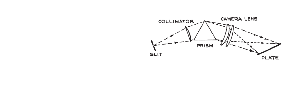
Fabry–Perot interferometers. From t he vacuum ultravio-
let (prism instruments c annot be used below ab out 1200
A
˚
) to the far infrared, grating instruments are much supe-
rior to comparable-size prism instruments in both resolving
power and luminosity. In recent years, the advantages of
grating instruments over prism instruments has virtually
eliminated the latter. This has primarily resulted because
of improvements in grating fabrication. Holographic plane
gratings have fewer and weaker ghosts than metal gratings,
and holographic curved gratings have allowed aberration
reduction in spectrometers. Apart from the minor incon-
venience of potential overlapping orders, grating instru-
ments are almost always to be preferred over prism
instruments. There is one exception worth noting: when a
monochromator is being used to observe some weak opti-
cal emission in the simultaneous presence of a strong laser
beam, unless the optical emission is too close in wave-
length to the laser for prism resolution to be adequate. In
this application, a prism avoids the problems of ghost
emission or grating scattering. A good prism has very
low scattered light. It is common to predisperse a light
beam with a prism before sending the beam into the
entrance slit of a monochromator, in order to avoid both
the overlapping-order problem and spurious signals from a
very strong light signal at another wavelength. Fabry–Perot
interferometers have very high resolution and luminosity,
but require careful and regular adjustment to maintain
high performance. They are used only where their very
high resolution is essential, frequently in conjunction with
a grating monochromator for pre-isolation of a narrow
spectral region.
A final point to note with regard to the use of grating
spectrometers: these instruments are polarization sensitive.
If unpolarized light strikes a grating, the diffracted light
will be partially polarized because the grating efficiency is
wavelength-, and S and P polarization-dependent.
4.7.2 Design of Spectrometers and
Spectrographs
The construction of monochromators and spectrographs is
a specialized undertaking. The availability of good com-
mercial instruments generally makes it unnecessary for
anyone but the enthusiast to contemplate their construction
in the laboratory. On the other hand, the principles that
underlie good design in a dispersing instrument are not
complex. Some essential features of such instruments
can be illustrated with reference to particular designs that
are used both in laboratory and commercial instruments.
Attention will be restricted to monochromators; spectro-
graphs are similar, apart from having an array detector or
photographic plate instead of an exit slit, as shown in
Figure 4.151. Spectrographs are also simpler in construc-
tion
because wavelength scanning is not required and all
optical components of the system remain fixed. The dis-
cussion here should also allow intelligent evaluation and
comparison of commercial instruments. For further details
of the many different instrument designs that have been
used for the construction of monochromators, spectro-
graphs and spectrophotometers, References
132,133
, The
Photonics Design and Applications Handbook
134
, and
the catalogs of instrument manufacturers should be con-
sulted.
Figure 4.152 shows a Littrow prism monochromator.
The
light from the input slit is collimated with an off-axis
paraboloidal mirror. The output wavelength is changed by
rotating the Littrow mirror. If the output wavelength must
change uniformly with rotation of a drive shaft, then the
rotation of the mirror requires a cam. Figure 4.153 shows a
Czerny–T
urner prism configuration. The collimating mir-
rors are spherical. In the geometry of Figure 4.153(a), the
coma
of one mirror compensates that of the other, while in
Figure 4.153(b) these comas are additive. The wavelength
is
changed by rotating the prism.
In any of these spectroscopic instruments, the optical
arrangement should be enclosed in a light-tight enclosure
Figure 4.151 Schematic diagram of a simple prism
spectrograph. (From R.J. Meltzer, ‘‘Spectrographs and
Monochromators,’’ in Applied Optics and Optical
Engineering, Vol. 5, R. Kingslake (Ed.), Academic Press,
New York, 1969; by permission of Academic Press.)
OPTICAL DISPERSING INSTRUMENTS 295
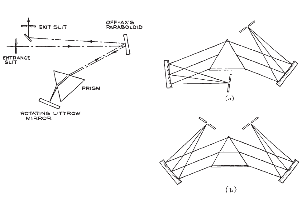
painted on its interior with black nonreflective paint. Table
4.10 lists the various ‘‘black’’ coatings that are available
for
this purpose and in any application where broad reflec-
tion over a range of angles from a surface must be mini-
mized. This helps to minimize scattered light. It is essential
that light passing through the entrance slit is not able to
reach the exit slit without going through the illuminating
optics and prism. To this end, it is common practice to
incorporate internal blackpainted baffles in the monochro-
mator enclosure. The most likely source of scattered light
is overillumination of the input collimator: input radiation
should not enter with an f/number smaller than that of the
monochromator. To check for stray light, visual observa-
tion through the exit slit in a darkened room when the
entrance slit is illuminated with an intense source will
reveal where additional internal baffles would be helpful.
Stray light is more likely to be a problem in a Littrow
arrangement than in a straight-through type, such as the
Czerny–Turner.
In the visible and near infrared, lens coll imating optics
can be used, as, for example, in the design shown in
Figure 4.151. Good lenses, such as camera lenses, should
be
used. Mirror collimating optics are useful over a much
broader wavelength region. For ult raviolet use they
should be aluminum overcoated with MgF
2
,andthey
are frequently of this type, even in instruments designed
for longer wavelengths.
Slit design is important in achieving high resolution.
Entrance and exit slits of equal width are generally used.
If the source is small, having a height much less than the
height of the prism or grating, parallel-sided slits are
adequate. Adjustable versions are available from Melles
Griot, Newport, and OptoSigma. Fixed slits can be easily
made using razor blades or purchased from Melles Griot or
National Aperture. If the source is high compared to the
height of the dispersing element, a straight entrance slit
produces a curved image at the exit slit. In the case of a
prism, this happens because light passing through the
prism at an angle inclined to the meridian plane suffers
slightly more deviation than light in the meridian plane.
Figure 4.153 Czerny–Turner monochromator
arrangements; (a) coma of one mirror compensates
that of the other; (b) comas are additive.
Figure 4.152 Littrow monochromator. (From R.J. Meltzer,
‘‘Spectrographs and Monochromators,’’ in Applied Optics and
Optical Engin eering, Vol. 5, R. Kingslake (Ed.), Academic
Press, New York, 1969; by permission of Academic Press.)
296 OPTICAL SYSTEMS
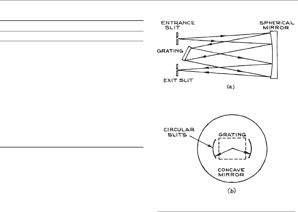
Light striking a grating in a plane that is not perpendicular
to the grating grooves sees an apparently smaller groove
spacing, and is consequently deviated more than light in
the plane perpendicular to the grating. To maintain high
resolution in the presence of image curvature, curved
entrance and exit slits should be used, each with a radius
equal to the distance of the slit from the axis of the system.
This slit arrangement is shown in Figure 4.154, which also
sho
ws a very good, and widely used, grating monochro-
mator design due to Fastie
135
(based on a design originally
described by Ebert
136
for use with a prism). It is also quite
common for the single spherical mirror in Figure 4.154 to
be
replaced by a pair, in which case the design becomes the
Czerny–Turner one. Such an arrangement is shown in Fig-
ure
4.155. In either case the wavelength is tuned by rotat-
ing
the grating. The wavelength variation at the exit slit is
much more nearly linear with grating rotation than with
prism rotation. If linearity is required, a cam, sine-drive, or
other such arrangement is used for rotating the grating or
prism.
133
In a Czerny–Turner grating instrument the
entrance and exit slits are generally arranged asymmetri-
cally with respect to the grating, as this allows coma to be
corrected in the working wavelength range. Czerny–Turner
monochromators are available from Edmund Optics, Gen-
esis Laboratory Systems (who now manufacture the for-
mer Jarrel-Ash line of spectrometers), Horiba Yobin Yvon,
McPherson, Minuteman Laboratories, Ocean Optics,
Princeton Intruments/Acton, and Thorlabs.
Grating monochromators for use in the vacuum ultra-
violet generally have a concave grating. Such a grating,
which has equally spaced grooves on the chord of a spher-
ical mirror, combines both dispersion and focusing in one
element. For maximum resol ution, both the object and
imageformedbyaconcavegratingmustbeonacircle
called the Rowland circle, whose diameter is the principal
radius of the s pherical surface on which the grating is
ruled, as shown in Figure 4.156. The use of a concave-
grating
monochromator (or spectrograph) entails mount-
ing grating and slits (or grating, slits, and photographic
plate) on a Rowland circle. Adjustment of the i nstrument
will involve moving the grating, slits, or plate on the
Figure 4.154 (a) Ebert–Fastie monochromator; (b) curved
entrance- and exit-slit configuration for use with the above.
Table 4.10 Black materials and coatings
Material Absorptivity
Anodized black 0.88
Carbon lampblack 0.84
Chemglaze black paint Z306 0.91
Delrin black plastic 0.87
Electro-optical industries 0.965
Mid-temperature black
coating (up to 200 °C)
Electro-optical industries 0.93
High-temperature black
coating (up to 1400 °C)
Martin black velvet paint 0.94
3M black velvet paint 0.91
Parsons black paint 0.91
Polyethylene black plastic 0.92
Anodized aluminum 0.84
OPTICAL DISPERSING INSTRUMENTS 297
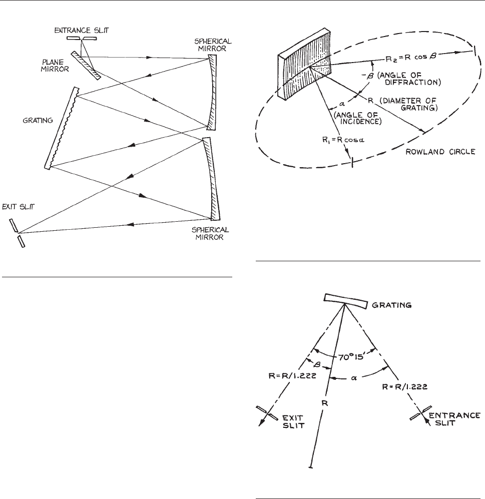
circle. Various mounting configurations, such as the
Abney, Eagle, Pasc hen, Rowland, and Wadsworth, and
grazing-incidence mounting have been used to accom-
plish this.
A convenient concave-grating design widely used
in vacuum-ultraviolet monochromator s is the Seya–
Namioka,
137,138
shown in Figure 4.157. In this arrange-
ment, by judicious choice of slit distances from the grating
and slit angular separation, the only adjustment needed
for wavelength adjustment is rotation of the grating. In
comparison with an ideal Rowland-circle mounting, only
a small resolution loss results over a wide wavelength
range. Vacuum-ultraviolet instruments possess the
added complication that all interior adjustments of the
instrument must be transmitted through the walls of the
vacuum chamber that houses the optical arrangement. Var-
ious kinds of rotary-shaft and bellows seals and magneti-
cally coupled drives exist for this purpose.
139
See also
Section 3.5.4.
Multiple
monochromators use multiple dispersing ele-
ments in series to obtain greater dispersion and/or lower
scattered light. For example, in a double-grating mono-
chromator, two diffraction gratings move simultaneously;
the desired diffracted wavelength from the first grating is
diffracted once again from the second grating before being
focused on the exit slit. The considerable reduction
in scattered light that can be obtained with multiple
Figure 4.156 Rowland circle of a concave diffraction
grating. For maximum resolution, both object and image
must be on the Rowland circle. R ¼ object (entrance-slit)
distance: R
2
¼ image (exit-slit) distance. (From R. J. Meltzer,
‘‘Spectrographs and Monochromators,’’ in Applied Optics
and Optical Engineering, Vol. 5, R. Kingslake (Ed.),
Academic Press, New York, 1969; by permission of
Academic Press.)
Figure 4.157 Layout of the Seya–Namioka
monochromator.
Figire 4.155 Arrangement of a Czerny–Turner grating
monochromator.
298 OPTICAL SYSTEMS

monochromators makes them particularly useful for ana-
lyzing weak emissions close in wavelength to a strong
emission, as in Raman spectroscopy. Instruments with as
many as four gratings in series are available commercially.
Grating monochromators, spectrographs, and spectropho-
tometers are available from many manufacturers,
31
includ-
ing American Holographic, Coherent Scientific, CVI
Spectral Products, Horiba Jobin-Yvon (formerly Spex or
Instruments SA), Minuteman Laboratories, Newport/
Oriel, Olis, Princeton Instruments/Acton, and Thermo Sci-
entific (which incorporates the old companies Jarrell-Ash,
Aminco-Bowman, Unicam, and Varian Associates). Fiber-
coupled spectrometers are manufactured by Ocean Optics,
Photon Control, and Stellar Net. These instruments either
consist of a complete spectrometer on a PC card or are
compact units connected to a computer through a USB
port. McPherson, Minuteman Laboratories, and Princeton
Instruments/Acton are noted for their vacuum instruments,
Coherent Scientific, Horiba Jobin-Yvon, and Princeton
Instruments/Acton for their multiple grating spectrome-
ters, and Genesis Laboratory Systems for their high-reso-
lution spectrometers and spectrographs.
Imaging Spectrographs [sometimes called optical mul-
tichannel analysers (OMAs )] image an entire spectrum
onto eit her a linear photodiode area (PDA) or onto a
linear CCD. These instruments often have the capability
for recording complete spectra from several sources at
once. Manufa cturers include Horiba Jobin-Yvon, Instru-
ment Systems GmbH, Olis, Nomadics, Princeton Instru-
ments/Acton, and Roper Scientific. Note that CCD arrays
are approximately 100 times more sensitive than PDAs,
so are best u sed f or the lowest light-level applications.
Change -coupled devices must be used with appropriat e
shutters or light modulation otherwise i mage ‘‘smear’’
will occur. This happens if new light falls on the array
while the previous deposited charge distribution i s being
read out.
Wavemeters are optical devices that are designed to pro-
vide direct electronic readout of the wavelength of mono-
chromatic radiation that is directed into them. They are
most frequently used in conjunction with a tunable laser
system. These convenient instruments incorporate a Fabry–
Perot or Fizeau interferometer. Manufacturers include Bris-
tol Instruments, Elliott Scientific, Holo-Spectra, MK Pho-
tonics, and Specialise Instruments Marketing.
4.7.3 Calibration of Spectrometers
and Spectrographs
To calibrate the wavelength scale of a spectrometer or spec-
trograph, the entrance slit is illuminated with a reference
source that has characteristic spectral features of accurately
known wavelength. It is quite common to mount a small
reference lamp – mercury, neon, and hollow-cathode iron
lamps are the most popular – near the entrance slit and use
a small remov able mirror or beamsplitter to superimpose the
spectrum of the reference on the unkno wn spectrum under
study. To calibrate a grating instrument through its various
orders, a helium–neon laser is ideal. If the slits are set to their
narrowest position and a low-power (< 1 mW) He–Ne laser
is directed at the entrance slit, the various grating settings that
transmit a signal (which can be safely observed by eye at the
exit slit) correspond to the wavelengths 0, 632.8 nm, 632.8 3
2 nm, 632.8 3 3 nm, and so on. By interpolation between the
observed v alues, a reliable calibration curve can be obtained
ev en for instruments operating far into the infrared.
The efficiency of the instrument at a given wavelength
can be determined with any suitable detector. A laser or
other narrow-band source at the desired wavelength illu-
minates the entrance slit, or a duplicate of it, and the trans-
mitted power is measured with the detector placed directly
behind the slit. A similar measurement is then made at the
exit slit of the whole instrument. The relative spectral effi-
ciency can be determined by illuminating the entrance slit
with a blackbody source. A lens should not be used for
focusing light on the entrance slit, as its collection and
focusing efficiency will vary with wavelength. The signal
at the output slit is then measured as a function of wave-
length with a spectrally flat detector, such as a pyroelectric
detector, thermopile, or Golay cell (see Section 7.10), and
normalized
with respect to the blackbody distribution.
4.7.4 Fabry–Perot Interferometers
and Etalons
Fabry–Perot interferometers and etalons are optical filters
that operate by multiple-beam interference of light
reflected and transmitted by a pair of parallel flat or coaxial
spherical reflecting interfaces. In its simplest form, an eta-
lon consists of a flat, parallel-sided slab of transparent
OPTICAL DISPERSING INSTRUMENTS 299
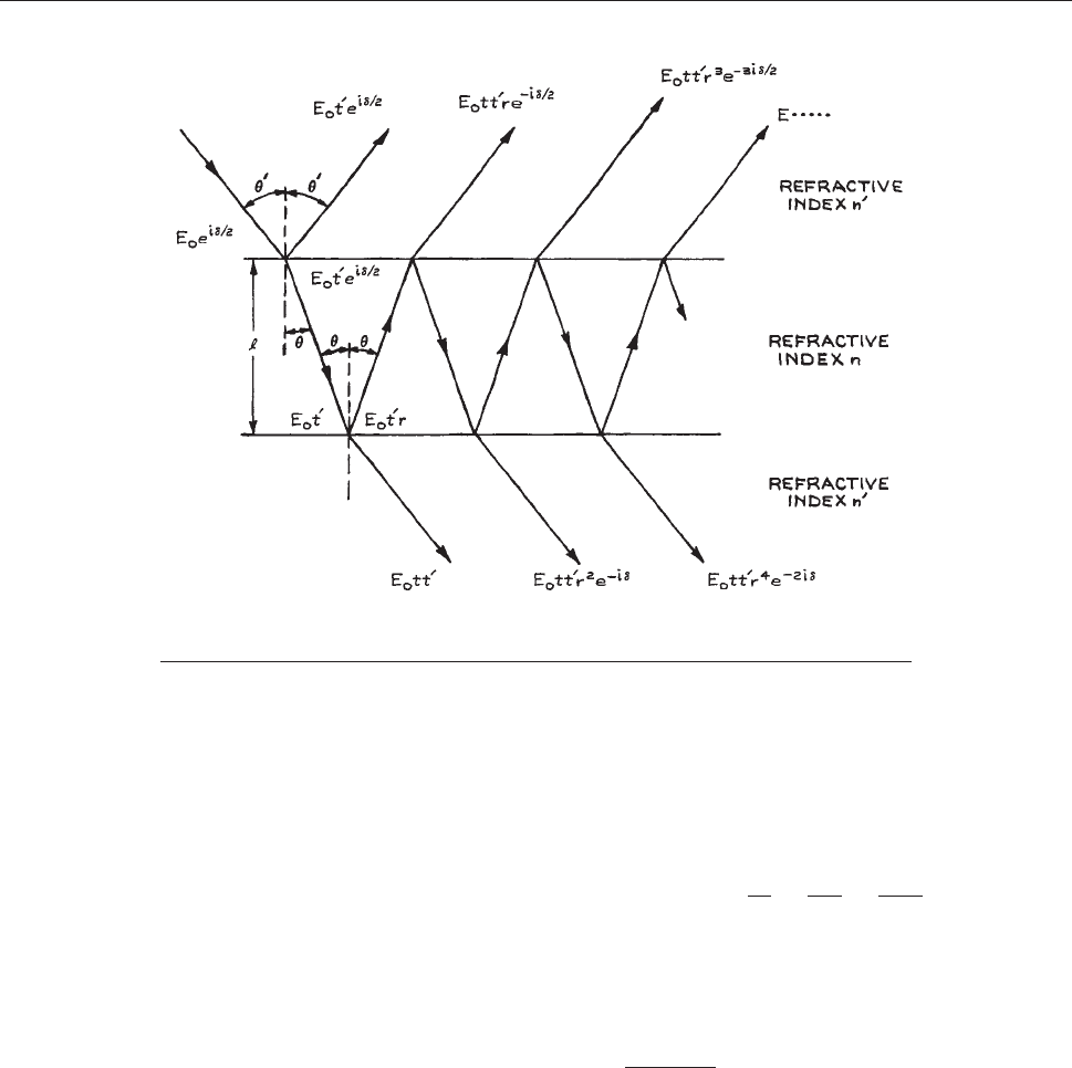
material, which may or may not have semireflecting coat-
ings on each face. An etalon may also consist of a pair of
parallel, air-spaced flat mirrors of fixed spacing. If the
reflective surfaces have adjustable spacing, or if their
effective optical spacing can be adjusted by changing the
gas pressure between the surfaces, the device is called a
Fabry–Perot interferometer. These devices can be ana-
lyzed by the impedance concepts discussed in Section
4.2.6, but it is instructive to discuss their operation from
the
standpoint of multiple-beam interference.
Figure 4.158 shows the successive reflected and transmit-
t
ed field amplitudes of a plane electromagnetic wave strik-
ing a plane-parallel Fabry–Perot etalon or interferometer at
angle of incidence h9. Although the reflection coefficients at
the two reflecting interfaces may be different, only the case
where they are equal will be analyzed. Almost all practical
devices are built this way. The optical-path difference
between successive transmitted waves is 2nl cos h,where
l is the interface spacing and n is the refractive index of the
medium between these interfaces (air, glass, quartz, or sap-
phire, for example). If refraction occurs at the reflecting
interfaces, h and h9 will be related by Snell’s law. The phase
difference between successive transmitted waves is:
d ¼ 2kl cos h þ2 e ð4:252Þ
where:
k ¼
2p
k
¼
2pn
k
0
¼
2pnv
c
0
ð4:253Þ
and e is the phase change (if any) on reflection.
The total resultant transmitted complex amplitude is:
E
T
¼ E
0
tt
0
þ E
0
tt
0
r
2
e
id
þ E
0
tt
0
r
4
e
2id
þ ...
¼
E
0
tt
0
1 r
2
e
id
ð4:254Þ
Here r and t are the reflection and transmission coefficients
of the waves passing from the medium of refractive index n
to that of refractive index n9 at each interface, r9 and t9 are
the corresponding coefficients for passage from n9 to n, and
E
0
is the amplitude of the incident electric field.
Figure 4.158 Paths of transmitted and reflected rays in a Fabry–Perot etalon. The complex
amplitude of the fields associated with the rays at various points is shown.
300 OPTICAL SYSTEMS
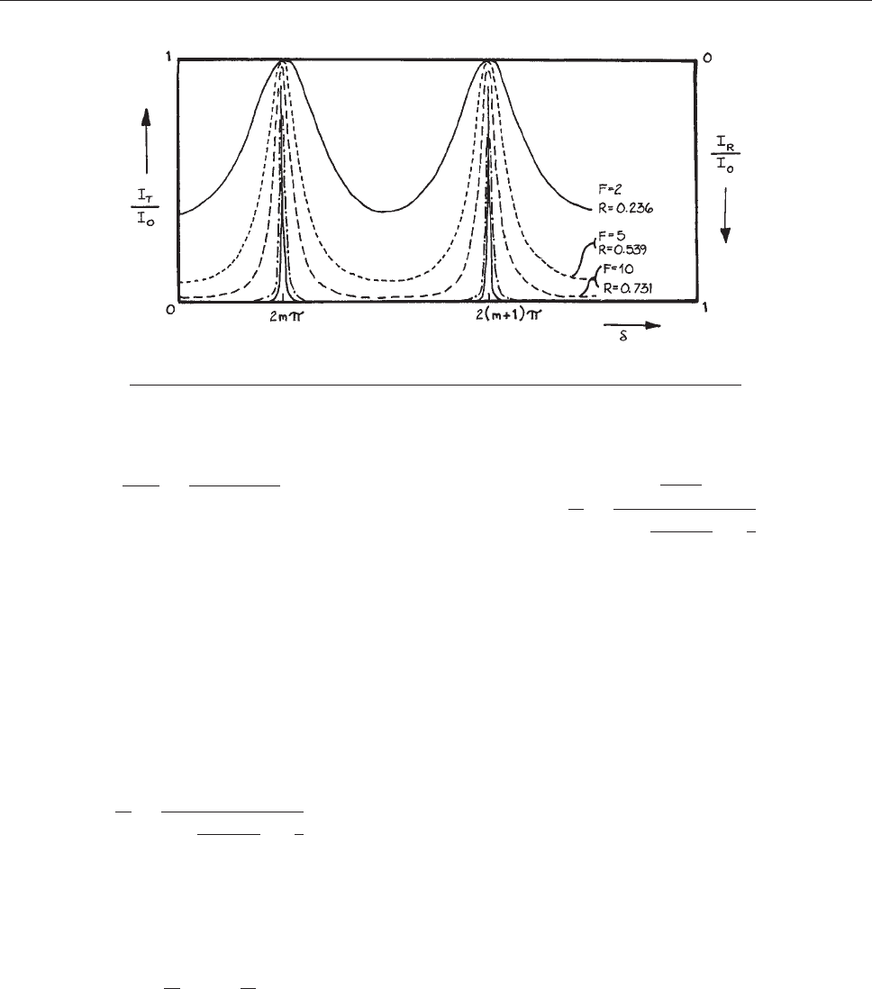
The total transmitted intensity is:
I
T
¼
jE
T
j
2
2Z
¼
I
0
jtt
0
j
2
j1 r
2
e
id
j
2
: ð4:255Þ
Here |tt9| ¼ T and |r|
2
¼ |r9|
2
¼ R, where T and R are the
transmittance and reflectance of each interface. If there is
no energy lost in the reflection process:
T ¼ 1 R ð4:256Þ
If the etalon had slightly absorbing reflective layers, this
would no longer be true; if each layer absorbed a fraction
A of the incident energy, then:
T ¼ 1 R A ð4:257Þ
If A ¼ 0, Equation (4.255) gives:
I
T
I
0
¼
1
1 þ
4R
ð1 RÞ
2
sin
2
d
2
ð4:258Þ
This variation of transmitted intensity with d is called an
Airy function and is illustrated in Figure 4.159 for several
v
alues of R. The variation of reflected intensity with d is
just the inverse of Figure 4.159, since:
I
R
I
0
¼ 1
I
T
I
0
ð4:259Þ
If A 6¼ 0, Equation (4.258) becomes:
I
T
I
0
¼
T
1 R
2
1 þ
4R
ð1 RÞ
2
sin
2
d
2
ð4:260Þ
In either case, maximum transmitted intensity results when:
d ¼ 2mp ð4:261Þ
where m is an integer. If the phase change on reflection is
neglected, this reduces to:
2l cos h ¼ mk ð4:262Þ
where k is the wavelength of the light in the medium
between the two reflecting surfaces (plates). In normal
incidence, transmission maxima result when:
l ¼ mk=2 ð4:263Þ
Even if the phase change on reflection is included, the
adjustment in spacing necessary to go from one transmis-
sion maximum to the next is one half-wavelength. Thus,
for example, the transmitted intensity as a function of plate
separation when a Fabry–Perot interferometer is illumi-
nated normally with plane monochromatic light is also
as shown in Figure 4.159. In an ideal Fabry–Perot device,
Figure 4.159 Transmission and reflection characteristics of a Fabry-Perot etalon.
OPTICAL DISPERSING INSTRUMENTS 301
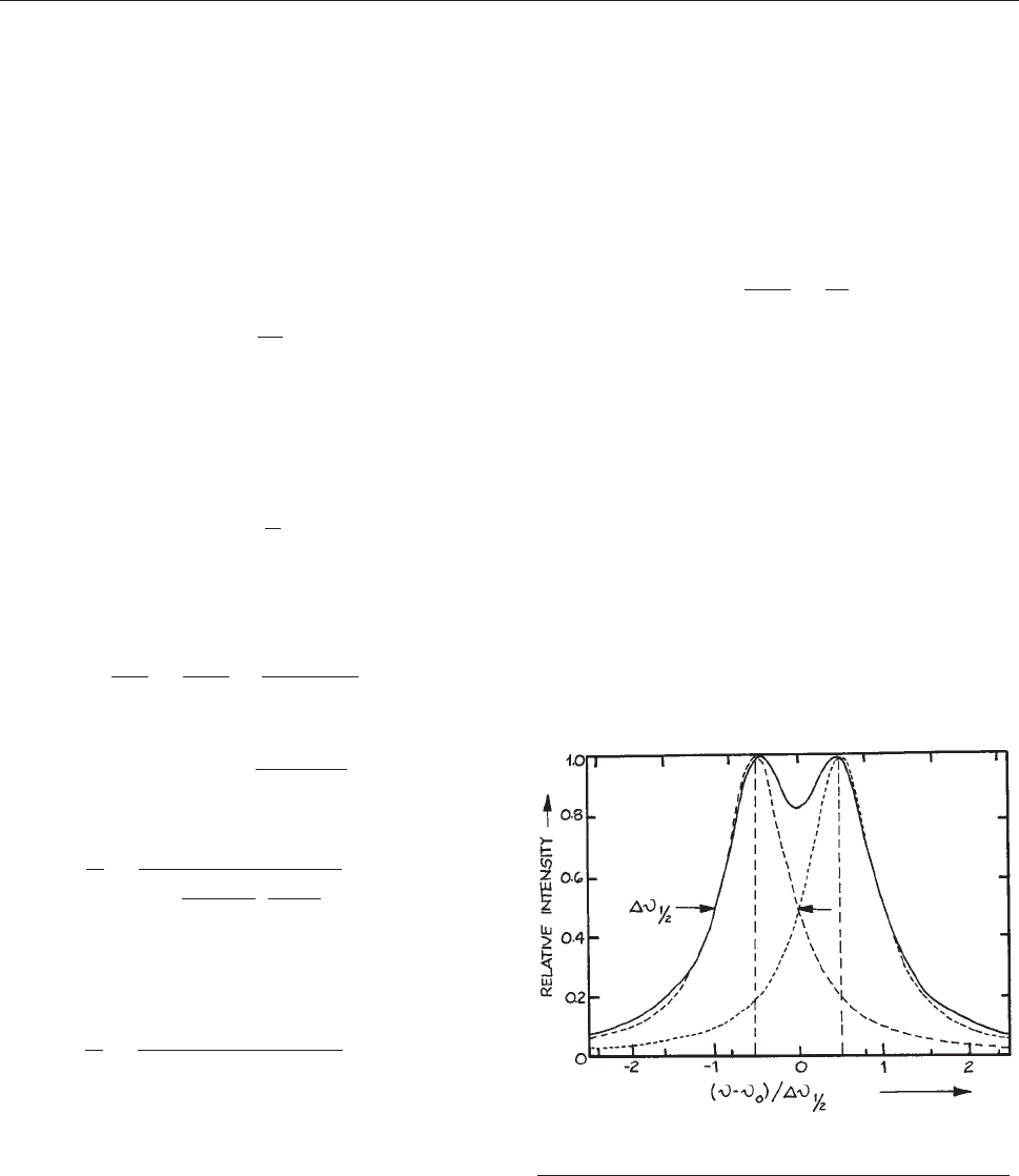
the overall transmittance at a transmission-intensity max-
imum is unity, whereas in a practical device, which will
invariably have some losses, the maximum overall trans-
mittance is reduced by a factor [T/(1 – R)]
2
. As is clear
from Figure 4.159, the transmission peaks of the device
become
very sharp as R approaches unity.
Free Spectral Range, Finesse, and Resolving
Power.
If a particular transmission maximum for fixed
I occurs for normally incident light of frequency v
0
, then:
v
0
¼
mc
2l
ð4:264Þ
where c is the velocity of light in the material between the
plates. Of course, the device will also show transmission
maxima at all frequencies v
0
6 pc/2l as well, where p is an
integer. The frequency between successive transmission
maxima is called the free spectral range:
Dv ¼
c
2l
ð4:265Þ
When R is close to unity, all phase angles d within a
transmission maximum differ from the value 2mp by only
a small angle. Thus, we can write:
d ¼
4pvl
c
¼
4pv
0
l
c
þ
4pðv v
0
Þl
c
ð4:266Þ
which can be written in the form:
d ¼ 2mp þ
2pðv v
0
Þ
Dv
ð4:267Þ
Equation (4.258) becomes:
I
T
I
0
¼
1
1 þ
4Rp
2
ð1 RÞ
2
v v
0
Dv
2
ð4:268Þ
Writing p
ffiffiffi
R
p
=ð1 RÞ¼F, where F is called the finesse,
the shape of a narrow transmission maximum can be writ-
ten as:
I
T
I
0
¼
1
1 þ 2ðv v
0
Þ=Dv
1=2
2
ð4:269Þ
Here Dv
1/2
, the full width at half maximum transmission of
the transmission peak, is given by:
Dm
1=2
¼ Dm=F ð4:270Þ
The resolving power of a Fabry–Perot device is a measure
of its ability to distinguish between two closely spaced
monochromatic signals. A good criterion for determining
this is the Rayleigh criterion, which recognizes two closely
spaced lines as distinguishable if their half-intensity points
on opposite sides of the two line shapes are coincident, as
shown in Figure 4.160. Thus, for a Fabry–Perot device the
resolving
power is:
<¼
v
Dv
1=2
¼
Fv
Dv
ð4:271Þ
It would appear that very high resolving powers can be
obtained by the use of high-reflectance plates (and con-
sequent high finesse values, as illustrated in Table 4.11)
and/or
large plate spacings (and consequent small free
spectral ranges). Additional practical considerations limit
how far these approaches to high resolution can act ually
be used.
Practical Operating Configurations and
Performance Limitations of Fabry–Perot
Systems.
The use of very high reflectance values to
obtain improved resolving power is limited by the ability
of the optical polisher to achieve ultraflat optical surfaces.
Very good-quality plates for use in the visible can be
obtained with flatnesses of k/200 over regions a few
Figure 4.160 Two monochromatic spectral lines just
resolved according to the Rayleigh criterion.
302 OPTICAL SYSTEMS

centimeters in diameter. Some claims of flatness in excess
of k/200 are also seen. These should be viewed with skep-
ticism – such a degree of flatness is extremely difficult to
verify. If the plates have surface roughness Ds, the average
error in plate spacing is
ffiffiffi
2
p
Ds. This gives rise to a spread in
the frequency of transmission maxima equal to:
Dv
s
’
mcDs
ffiffiffi
2
p
l
2
’
ffiffiffi
2
p
v
0
Ds
l
ð4:272Þ
Thus the flatness-limited finesse is:
F
s
¼
Dv
Dv
s
¼
1
ffiffiffi
2
p
Dv
v
0
l
Ds
¼
k
2
ffiffiffi
2
p
Ds
ð4:273Þ
For example, two plates with surface roughness of k/200
would have a flatness-limited finesse of about 71. The use
of super mirrors has allowed finesse values to 30 000 to be
achieved. In practice, Fabry–Perot plates may not be ran-
domly rough, and their stated flatness figure may represent
the average deviation from parallelism of the two plates. In
this case, the parallelism-limited finesse is:
F
q
¼
k
2Ds
ð4:274Þ
where Ds is the deviation from parallelism over the used
aperture of the system. Thus, for example, with a 1 cm aper-
ture, a 1/100 arc-second deviation from parallelism would
imply Ds ¼ 4.84 nm and a parallelism-limited finesse of only
56 at 546 nm. Depending on the definition of what is meant
by surface roughness and deviation from parallelism, Equa-
tions (4.273) and (4.274) may take slightly different forms.
139
Fabry–Perot plates must be held very nearly parallel to
achieve high resolution. Also, their separation should not
be allowed to drift. A random variation of Ds will limit the
finesse, as predicted by Equation (4.273). A fractional
length change of 10
–6
in a 1 cm spacing Fabry–Perot
device will limit the finesse to only about 27. Thus it must
be isolated from vibrational interference to achieve high
finesse. Further, if the frequencies of the transmission max-
ima are not to drift, the change in plate spacing due to
thermal expansion must be minimized by constructing
the device of low-expansion materials such as Invar,
141
Superinvar,
142
fused silica,
143
or special ceramics.
144
The resolving power of a Fabry–Perot system is also
limited by the range of angles that can be transmitted
through the instrument. One popular configuration is shown
in Figure 4.161. A small source, or light from an extended
source that passes through a small aperture, is collimated
by a lens, passes through the interferometer, and is focused
onto a second small aperture in front of a detector. The
maximum angular spread of rays passing through the sys-
tem will be governed by the aperture sizes W
1
and W
2
and
the two focal lengths f
1
and f
2
. In the paraxial-ray
Table 4.11 Properties of Fabry-Perot etalons
Plate Separation
l (cm)
Reflectance R (%) Free Spectral Range
Dt ¼c/2Z Hz
Finesse
F ¼ p
ffiffiffiffiffiffiffiffiffi
R
1RðÞ
q
Resolving Power
R ¼Ft/Dm
0.1 80 1.5 3 10
11
14 5.6 3 10
4
0.1 90 1.5 3 10
11
30 1.2 3 10
5
0.1 95 1.5 3 10
11
61 2.44 3 10
5
0.1 99 1.5 3 10
11
313 1.25 3 10
6
1.0 80 1.5 3 10
10
14 5.6 3 10
5
1.0 90 1.5 3 10
10
30 1.2 3 10
6
1.0 95 1.5 3 10
10
61 2.44 3 10
6
1.0 99 1.5 3 10
10
313 1.25 3 10
7
10.0 80 1.5 3 10
9
14 5.6 3 10
6
10.0 90 1.5 3 10
9
30 1.2 3 10
7
10.0 95 1.5 3 10
9
61 2.44 3 10
7
10.0 99 1.5 3 10
9
313 1.25 3 10
8
Note: Properties shown are at 500 nm (600 THz).
OPTICAL DISPERSING INSTRUMENTS 303

approximation, the angular width 2Dh of the paraxial-ray
bundle that comes from, or is delivered to, an aperture of
diameter W is equal to the angular width 2Dh9 that traverses
the system, as illustrated in Figure 4.162. In this case:
Dh ’ W=2f ð4:275Þ
In Figure 4.161 the resolving power will be limited by
W
1
/f
1
or W
2
/f
2
, whichever is the larger. The transmitted
frequency spread associated with an angular spread Dh
around the normal direction is, from Equations (4.262)
and (4.264):
Dv
1=2
¼ v
0
ðDhÞ
2
=2 ð4:276Þ
The corresponding aperture-limited finesse is:
F
A
¼
k
lðDhÞ
2
¼
4kf
2
lW
2
ð4:277Þ
For example, using a 1 mm diameter aperture, a 10 cm
focal-length lens, and a 1-cm air-spaced Fabry–Perot
device at 546.1 nm, the aperture-limited finesse is 218.
The operating conditions of a Fabry–Perot system should
be arranged so that F
A
is at least three times larger than the
desired operating finesse, which usually is ultimately
limited by the flatness-limited finesse. The apertures in
Figure 4.161 should be circular and accurately coaxial
with both lenses, or the aperture finesse will be further
reduced. If the limiting aperture (either a lens or the
Fabry–Perot device itself) is D, there is also a diffraction
limit to the finesse, which on axis is:
F
D
¼
2D
2
knl
: ð4:278Þ
At the pth fringe off axis:
F
D
¼
D
2
2pknl
ð4:279Þ
where n is the refractive index of the material between
the plates. The overall finesse of a Fabry–Perot system,
F
l
, is related to t he individual contributions to the finesse,
F
i
,by
F
2
l
¼ +
i
F
2
i
ð4:280Þ
Figure 4.161 (a) Operating scheme for a Fabry–Perot
interferometer, using collimated light; (b) detail of typical
plate configuration (the wedge angle of the reflecting plates
is exaggerated).
Figure 4.162 Angular factors involved in the collection
of light transmitted through a Fabry–Perot interferometer
by a circular aperture. In the paraxial-ray
approximation, Dh9 ¼ Dh.
304 OPTICAL SYSTEMS

In the operating configuration of Figure 4.161, if the plate
spacing is fixed, then with a broad-band source, all frequen-
cies that satisfy Equation (4.280) will be transmitted. These
fr
equencies become more closely spaced as the plate sepa-
ration l is increased. There is a concomitant increase in
resolution, but this may not prove useful if any of the spec-
tral features under study are broader than the free spectral
range. In this case, simultaneous transmission of two broad-
ened spectral features always occurs. For example, for two
lines of wavelength k
1
and k
2
and of FWHM Dk ,itis
usually possible to find two integers m
1
and m
2
such that:
m
1
k
0
1
¼ 2l, jk
0
1
k
1
j& Dk
m
2
k
0
2
¼ 2l, jk
0
2
k
2
j& Dk
ð4:281Þ
Thus, for isolated, high-resolution studies of the spectral
feature at k
1
, say, all potential interference features such as
k
2
must be filtered out. This is done with a color or inter-
ference filter, or a prism or grating monochromator, before
the signal is sent to the interferometer. The choice of pre-
filtering element will depend on the relative wavelength
spacing of k
1
and k
2
The optical throughput of filters can
be very high, 50% or more, but will not allow prefiltering
of lines closer than a few nanometers. When very high
throughput coupled with high resolution is essential, one
or more additional Fabry–Perot devices of appropriate free
spectral range can be used. For example, an etalon of spac-
ing 0.01 mm has a free spectral range of about 15 nm. If
it has a finesse of 50, its useful transmission bandwidth is
0.3 mn. Such an etalon could be coupled with etalons of
spacing 0.1 mm and 1 mm with similar finesse to isolate a
band only 0.003 nm wide from an original relatively broad
frequency band transmitted through a filter. The final
transmitted wavelength of such a combination of etalons
can be tuned by tilting.
The wavelength of maximum transmission of a single
etalon varies as:
k ¼ k
0
cos h ð4:282Þ
where k
0
is the wavelength for maximum transmission in
normal incidence. In the interferometer arrangement
shown in Figure 4.161(a), wavelength scanning can be
ac
complished in two ways: by p ress ure scann ing, or by
adjusting the axial position of one of the plates with a
piezoelectri c transducer.
145
To accomplish pressure scan-
ning, the interferometer is mounted in a vacuum- or
pressure-tight housing into which gas can be admitted
at a slow ste ady rate. The resultant change of refractive
index of the gas between the plates, which is approxi-
mately linear with pressure, ca uses a continuous, unidir-
ectional scanning of the center transmitted frequency.
The interferometer should b e mounted freely within
the housing so that the pressure differential between the
interior and exterior of the housing causes no deformation
of th e interf erome ter. Pressure scanning is no t conve-
nient where rapid or bidirectional scanning is required.
Because no geometrical dimensions of the interferometer
change during the scan, n o c h ange in finesse should oc cur
during scanning.
Piezoelectric scanning is very convenient, but the trans-
ducer material must be specially selected to give uniform
translation of the moving plate without any tilting – which
would cause finesse reduction during scanning. If separate
piezoelectric transducers
145
are mounted on the kinematic-
mounted alignment drives of the plate holders, it is possi-
ble to trim the finesse electronically after good mechanical
alignment has been achieved by micrometer adjustment.
The alignment of the plates during scanning can be main-
tained with a servo system.
146,147
A Fabry–Perot eta lon can be used in the configuration
shown in Figure 4.163 to give a high-resolution display of
a
narrow-band s p ect ral featur e that cannot be displayed
with a scanning interferometer because (for example)
the optical signal is a short pulse. In the arrangement
shown in Figure 4.16 3, all rays from a monochromatic
source
that are incident at angle h
m
on the plates will be
transmitted and brought to a focus in a bright ring on a
screen if:
cos h
m
¼
mk
2l
ð4:283Þ
In the paraxial approximation, h
m
is a small angle and the
radius q
m
of a ring on the screen is:
q
m
¼ f h
m
ð4:284Þ
which can be written as:
q
m
¼ f
ffiffiffiffiffiffiffiffiffiffiffiffiffiffiffi
2
mk
l
r
ð4:285Þ
OPTICAL DISPERSING INSTRUMENTS 305
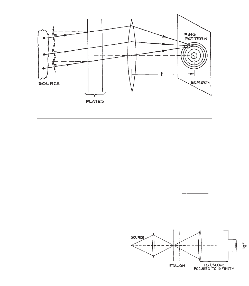
The radius of the smallest ring corresponds to the largest
integer m, for which mk /2l < 1. Successive rings going out
from the center of the pattern correspond to integers m –1,
m – 2, and so on.
If there is a bright spot at the center of the ring pattern,
the radius of the pth ring from the center is:
q
p
¼ f
ffiffiffiffiffi
pk
l
r
: ð4:286Þ
This ring will be diffuse because of the finite finesse of the
etalon, even if the source is highly monochromatic. The
FWHM at half maximum intensity of the pth ring in this
case is:
Dq
p
¼
q
p
2pF
ð4:287Þ
which can be verified by expanding Equation (4.260) in the
angle h. This ring width is the same as would be produced
by a source of FWHM Dk ¼ k
2
/2lF.
Equation (4.287) predicts that the total flux through each
ring of the pattern will be identical, since the area of each
ring is:
DA ¼ 2pq
p
Dq
p
¼ pf
2
=2lF ð4:288Þ
The ratio of ring width to ring spacing for the pth ring in
the pattern is:
Dq
p
q
p þ1
q
p
¼ 2Fp 1
ffiffiffiffiffiffiffiffiffiffiffiffiffi
1 þ
1
p
s
!"#
1
ð4:289Þ
which is close to 1/F except for the first few rings. Thus
observation of the ring pattern from a quasimonochromatic
source will yield its approximate bandwidth Dk as:
Dk ’
k
2l
Dq
q
p þ1
q
2
ð4:290Þ
A convenient way of making a qualitative visual observa-
tion of this kind is to use an etalon in conjunction with a
small telescope, as shown in Figure 4.164.
Figure 4.164 Arrangement for visual observation of
Fabry–Perot fringes.
Figure 4.163 Arrangement for observing a ring interference pattern with a
Fabry–Perot etalon.
306 OPTICAL SYSTEMS

Luminosity, Throughput, Contrast Ratio, and
E
´
tendue.
The luminosity of a Fabry–Perot system is, as
already mentioned, much higher than that of any prism or
grating monochromator. In the arrangement of Figure
4.161, the luminosity is:
U ¼
T
1 R
2
E
e
ðkÞS
pW
2
2
4f
2
ð4:291Þ
where pW
2
2
/4f
2
is the solid angle subtended by the output
circular aperture at the output focusing lens, and S is the
illuminated area of the plates. If the system has an aper-
ture-limited finesse, then, from Equation (4.277) the lumi-
nosity
becomes:
U ¼
T
1 R
2
E
e
ðkÞ
pkS
qF
A
ð4:292Þ
which can be written in terms of the resolving power < as:
U ¼
T
1 R
2
E
e
ðkÞ
2pS
<
ð4:293Þ
The factor [T/(1 – R)]
2
is called the throughput of the
system. To compare the luminosity predicted by Equation
(4.293) with that of a grating, we shall assume that the
throughput
of the Fabry–Perot system is equal to the cor-
responding efficiency factor T of the grating in Equation
(4.240). In this case, for identical resolving powers <,
from
Equations (4.293) and (4.240), we have:
UðF:P:Þ
UðgratingÞ
¼
pS
ðA sin bÞðl=f
2
Þ
ð4:294Þ
where l/f
2
is the angular slit height at the output-focusing
element of the grating monochromator. For a blaze angle
of 30° and equal Fabry–Perot aperture and grating area:
UðF:P:Þ
UðgratingÞ
¼
p
l=f
2
ð4:295Þ
For a 0.3 m focal length grating instrument and a slit height
of 3 cm (which is a typical maximum value for a small
instrument of this size), the luminosity ratio is 71.4. This
probably represents an optimistic comparison as far as the
grating instrument is concerned, since high-resolution gra-
ting monochromators typically have focal lengths in
excess of 0.75 m.
The contrast ratio of a Fabry–Perot system is defined as:
C ¼
ðI
T
=I
0
Þ
max
ðI
T
=I
0
Þ
min
ð4:296Þ
which from Equation (4.258) clearly has the value:
C ¼
1 þ R
1 R
2
¼ 1 þ
4F
2
p
2
ð4:297Þ
The e
´
tendue U of a Fabry–Perot system is a measure of its
light-gathering power for a given frequency bandwidth
Dv
1/2
. It is defined by:
U ¼ XS ð4:298Þ
where A is the area of the plates and X is the solid angle
within which incident rays can travel and be transmitted
with a specified frequency bandwidth. From Equation
(4.276), since X ¼ pDh
2
:
Dv
1=2
¼
v
0
X
2p
ð4:299Þ
Therefore:
U ¼ XS ¼
2pDv
1=2
v
0
pD
2
4
ð4:300Þ
which can be written in the form:
U ¼ XS ¼
p
2
D
2
k
4lF
1
ð4:301Þ
Spherical Mirror Fabry–Perot Interferometers.
Fabry–Perot interferometers with spherical concave
mirrors are generally used in a confocal arrangement, as
shown in Figure 4.165. In this configuration the various
chara
cteristics of the interferometer can be summarized as
follows:
I
T
I
0
max
¼
T
2
2ð1 RÞ
2
ð4:302Þ
DvðFSRÞ¼c=4l ð4:303Þ
reflectivitylimited finesse ¼
p
ffiffiffi
R
p
ð1 RÞ
ð4:304Þ
OPTICAL DISPERSING INSTRUMENTS 307
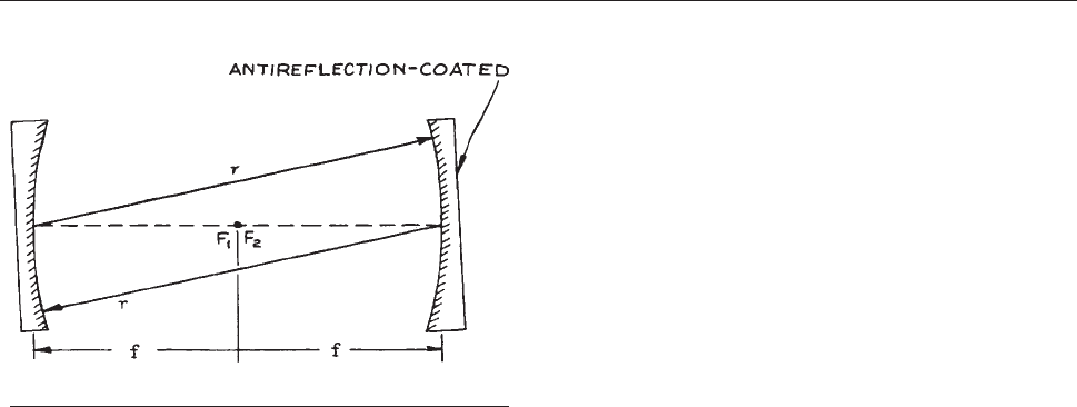
The approximate optimum radius of the apertures used
in an arrangement similar to Figure 4.161 is 1.15 (kr
3
/f/)
1/4
,
where r is the radius of the spherical mirrors. Fabry–Perot
interferometers with spherical mirrors can achieve very
high finesse values.
The characteristics of all the possible combinations of
two spherical mirrors that can be used to form a Fabry–Perot
interferometer have been very extensively studied in con-
nection with the use of such mirror arrangements to form
the resonant cavities of laser oscillators.
14–16
In that appli-
cation, these spherical-mirror resonators support Gaussian
beam modes, and it is with such Gaussian beams that high-
est performance can be achieved with a spherical-mirror
Fabry–Perot interferometer. Thus, a confocal Fabry–Perot
interferometer is ideal for examining the spectral content of
a Gaussian laser beam. The beam to be studied should be
focused into the interferometer with a lens that matches
the phase-front curvature and spot size of the laser beam
to the radius of the Fabry–Perot mirror and the spot size of
the resonant modes. (See Section 4.2.7.)
4.7.5 Design Considerations for
Fabry–Perot Systems
Fabry–Perot interferometers and etalons are extremely
sensitive to angular misalignment and fluctuations in plate
spacing. Consequently, their design and construction are
more demanding than for other laboratory optical instru-
ments. The plates must be extremely flat, as already
mentioned, and must be held without any distortion in
high-precision alignment holders. The plate spacing must
be held constant to about 1 nm in a typical high-finesse
device for use in the visible, and the angular orientation
must be maintained to better than 0.01 second of arc.
Small-plate-spacing etalons are generally made commer-
cially by optically contacting two plates to a precision
spacer, or spacers, made of quartz. Such etalons are avail-
able from CVI Laser, II-VI Infrared, Michigan Aerospace,
OFR, Research Electro-Optics, Rocky Mountain Instru-
ment Co., TecOptics, Scientific Solutions, and SLS Optics,
among others. Etalons of thickness in excess of 1 or 2 mm
for use in the visible can be made from solid plane-parallel
pieces of quartz or sapphire with dielectric coatings on
their faces, or from materials, such as germanium or zinc
selenide, for infrared use. Fabry–Perot interferometer
plates are almost always slightly wedge-shaped and anti-
reflection-coated on their outside faces to eliminate
unwanted reflections, as shown in Figure 4.161(b). To pre-
vent distortion of the plates they should be kinematically
mounted in their holders. A good way to do this is to use
three quartz or sapphire balls cemented to the circumfer-
ences of the plates and held in ball, slot, and plane loca-
tions with small retaining clips. For further details see
Section 1.7.1 and Figures 1.52 and 1.53.
For the construction of Fabry–Perot interferometers,
low-expansion materials should be used. The plate holders
can be held at a fixed spacing by having them spring-
loaded against three quartz or ceramic spacer rods or by
the use of an Invar or Super-Invar spacer structure.
After a Fabry–Perot interferometer is aligned mechan-
ically, it will creep slowly out of alignment, because of the
easing of micrometer threads, for example. The alignment
can be returned by having a piezoelectric element
145
incor-
porated in each plate-orientation adjustment screw.
Fabry–Perot interferometers are made commercially by
Bernhard Halle Nachfl. GmbH, Bristol Instruments (who
still provide service and parts for Burleigh interferome-
ters), Hovemere, SSI, and Thorlabs.
The Fizeau interferometer is closely related to the
Fabry–Perot, except that one of the mirrors is made totally
reflecting and a beamsplitter is used to extract the interfer-
ing waves. They measure the phase difference between a
reference surface and the object under test, as shown sche-
matically in Figure 4.166. These interferometers are
commonly used to test the flatness of optical surfaces.
Figure 4.165 Confocal Fabry–Perot interferometer.
308 OPTICAL SYSTEMS
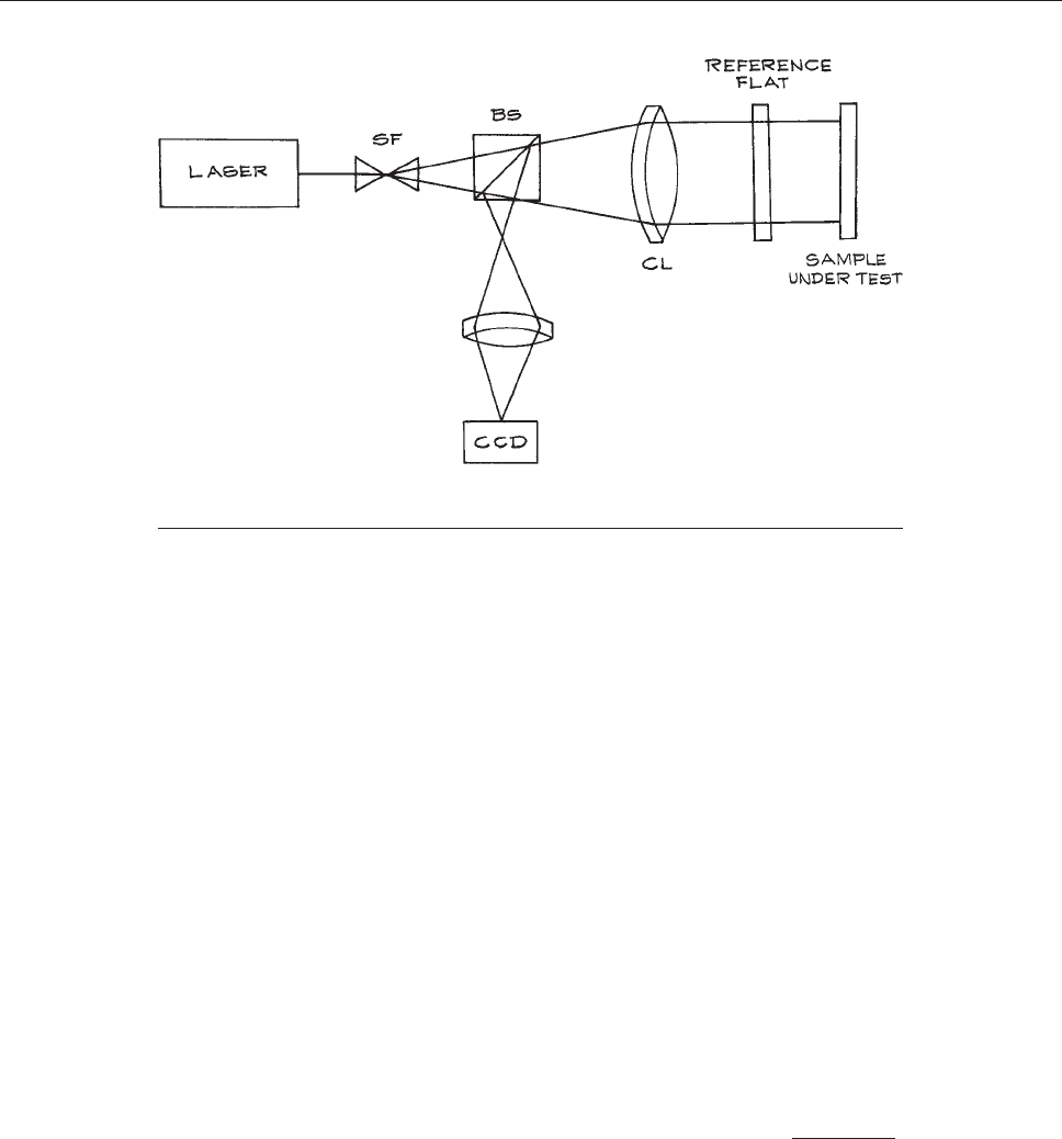
They are available commercially from 4D Technology,
Davidson Optronics, Logitech, Moeller-Wedel Optical
GmbH, Sigma Koki Co, Silo, and Zygo.
4.7.6 Double-Beam Interferometers
In a double-beam interferometer, waves from a source are
divided into two parts at a beamsplitter and then recom-
bined after traveling along different optical paths. The
most practically useful of these interferometers are the
Michelson and the Mach–Zehnder.
The Michelson Interferometer. The operation of a
Michelson interferome ter can be illus trated with
reference to Figure 4.167. Light from a n extended
source
is divided at a beamsplitter and sent to two plane
mirrors M
1
and M
2
. If observations of a broad-band
(temporally incoherent) source are being made, a
compensating plate of the same material and thickness
as the beamsplitter is included in arm 2 of the
interferometer. This p late compensates for the two
additional traverses of the beamsplitter substrate made
by the beam in arm 1. Because of the dispersion of the
beamsplitter material, it produces a phase difference t hat
is wavelength-dependent, and without the compensating
plate, interference fringes would not be observable with
broad-band illumination (such as white light).
A maximum of illumination results at angle h in Figure
4.167 if the phase difference between the two beams com-
ing
from M
1
and M
2
is an integral multiple of 2p.IfM9
2
represents the location of the reflection of M
2
in the beam-
splitter, the condition for a maximum at angle h is:
2l cos h ¼ mk: ð4:305Þ
The positioning of M
1
at M
2
corresponds to l ¼ 0, m ¼ 0. If
the output radiation is focused with a lens, a ring pattern is
produced. A clear ring pattern is only visible if:
2l cos h & l
c
ð4:306Þ
where l
c
, is the coherence length of the radiation from the
source. The clearness of the rings is usually described in
terms of their visibility V, defined by the relation:
V
max
¼
I
max
I
min
I
max
þ I
min
ð4:307Þ
To obtain a ring-shaped interference pattern, M
1
and M
2
must be very nearly parallel; otherwise a pattern of curved
Figure 4.166 Fizeau interferometer. SF – spatial filter, BS – beamsplitter cube,
CL – collimating lens.
OPTICAL DISPERSING INSTRUMENTS 309
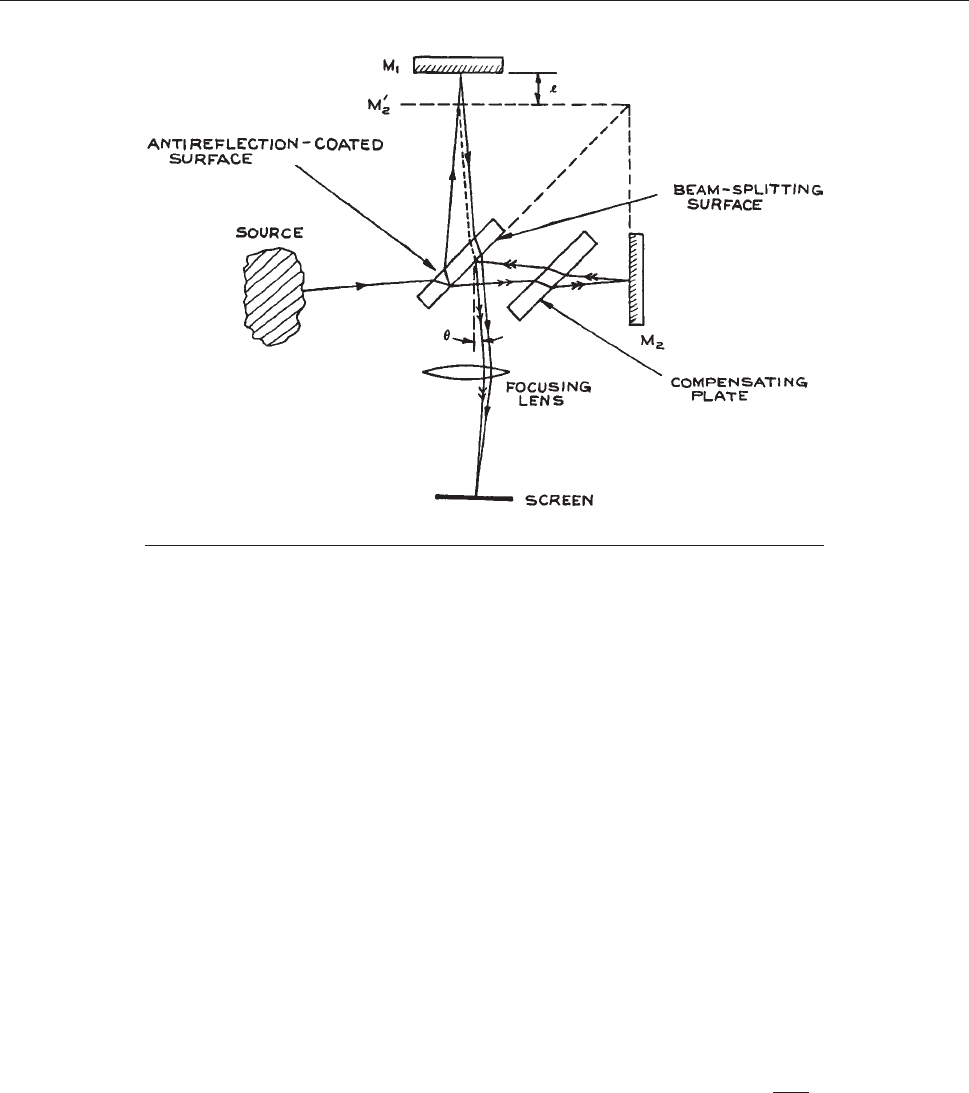
dark and light bands will result. To study the fringes, mirror
M
1
must be scanned in a direction perpendicular to its sur-
face. This can be done with a precision micrometer, or a
piezoelectric transducer, if only small motion is desired.
Because interference fringes are only observed with a
broad-band source illuminating a Michelson (or other dou-
ble-beam) interferometer when the two interferometer arms
are of almost equal length, this mode of operation is extra-
ordinarly sensitive. Such ‘‘white-light interferometry’’
forms the basis of a number of sensor systems for phenom-
ena such as vibration, temperature, and pressure.
149,150
In practice, Michelson interferometers are rarely used in
the configuration shown in Figure 4.167, but are used
instead
with collimated illumination (a laser beam, or par-
allel light obtained by placing a point source at the focal
point of a converging lens) as shown in Figure 4.168.In
this
case, the output illumination is (almost) perfectly uni-
form, being a maximum if:
2l ¼ mk ð4:308Þ
where 2l is the path difference between the two arms.
If monochromatic illumination of angular frequency x
is used, we can write the fields of the waves from arms 1
and 2 as:
V
1
¼ V
0
e
iðxt/
1
Þ
V
2
¼ V
0
e
iðxt/
2
Þ
ð4:309Þ
where it is assumed that the beamsplitter divides the inci-
dent beam into two equal parts. /
1
and /
2
are the optical
phases of these two beams, which are dependent on the
optical path lengths traveled in arms 1 and 2.
The output intensity is:
I } ðV
1
þ V
2
ÞðV
1
þ V
2
Þð4:310Þ
which gives
I ¼ I
0
1 þ cosð/
2
/
1
Þ½
¼ I
0
1 þ cos
4pvl
c
ð4:311Þ
Figure 4.167 Michelson interferometer.
310 OPTICAL SYSTEMS
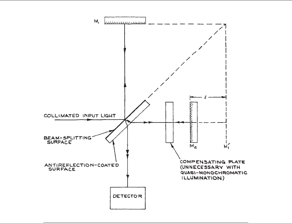
in which I
0
is the intensity of the light from one arm alone.
Suppose an optical component such as a prism or lens is
placed in one arm of the interferometer, as shown in Figure
4.
169, with the plane mirror replaced by an appropriate radius
sp
herical mirror in the case of the lens, and quasi-monochro-
matic illumination is used. Then the output fringe pattern will
rev eal inhomogeneities and defects in the inserted component.
A Michelson interferometer used in this way for testing opti-
cal components is called a Twyman–Green interferometer.
11
Equation (4.302) illustrates why Michelson (and all
other double-beam) interferometers are not directly suit-
able for spectroscopy. The distance the movable mirror
must be adjusted to go from one maximum to the next is:
Dl ¼ k=2 ð4:312Þ
The distance required to go from a maximum- to a half-
maximum-intensity point is:
Dl ¼ k=8 ð4:313Þ
Thus the effective finesse is only 4: sharp spectral peaks
with monochromatic illumination are not obtained, as they
are in multiple-beam interferometers.
Fourier Transform Spectroscopy. In an arrange-
ment such as Figure 4.168, if the movable mirror is
scanned
at a steady velocity v, the resultant intensity as a
function of position can be used to obtain considerable
information about the spectrum of the source. If the
Figure 4.168 Simple Michelson interferometer for use with collimated input radiation.
OPTICAL DISPERSING INSTRUMENTS 311
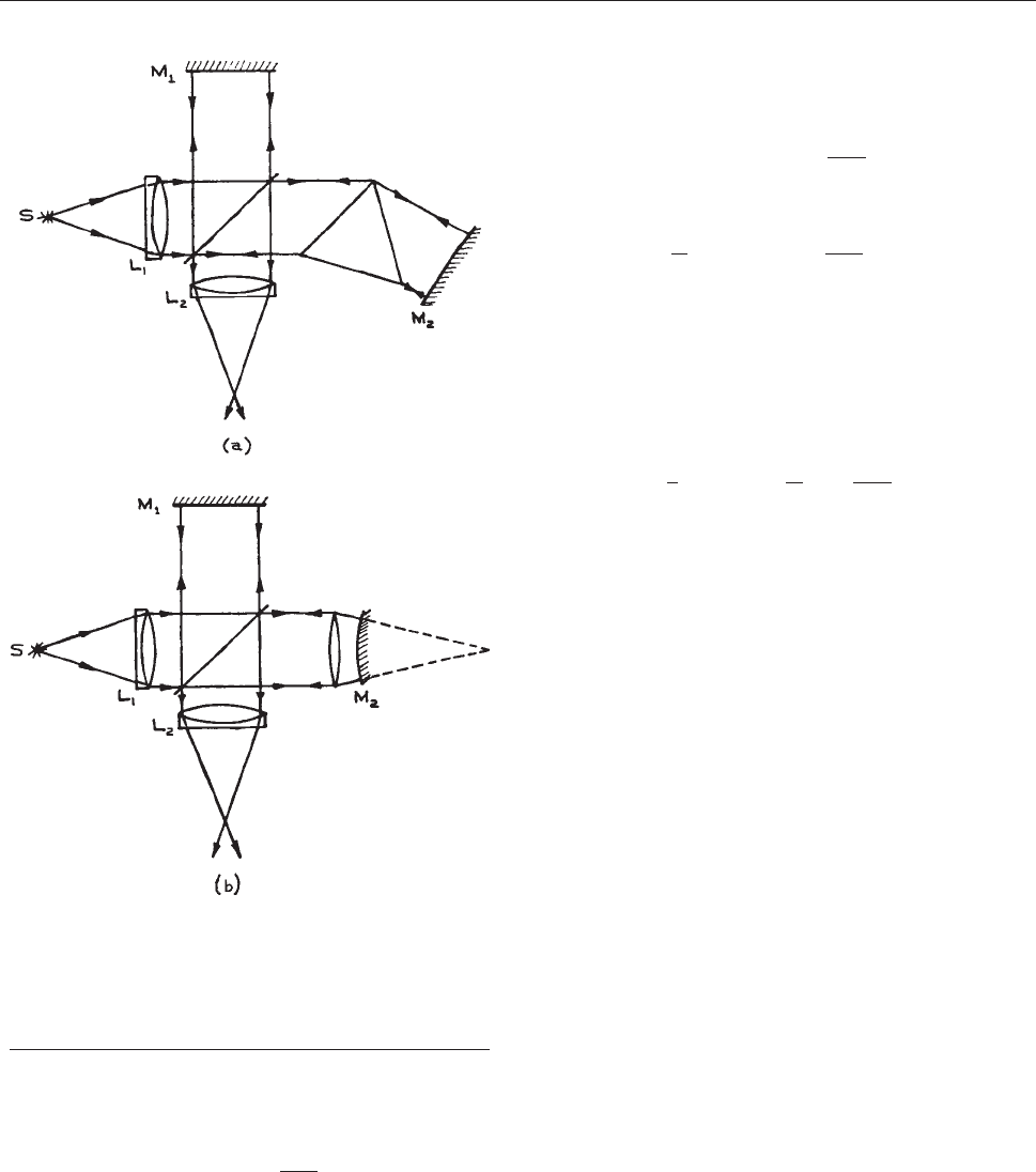
source has intensity I(m)atm, the contribution to the
intensity from the small band dm at v is:
I
m
ðlÞ¼IðmÞ 1 þ cos
4pml
c
dm ð4:314Þ
where l ¼ mt. The total observed output from the full spec-
trum of the source is:
IðlÞ¼
ð
‘
m ¼0
IðmÞ 1 þ cos
4pml
c
dm
¼
I
0
2
þ
ð
‘
m ¼0
IðmÞcos
4pml
c
dm
ð4:315Þ
The second term on the second line is essentially the
cosine transform of I(v). Thus I(v) can be found as the
cosine transform of I(l)–(I
0
/2):
IðvÞ¼
2
c
ð
‘
l ¼0
IðlÞ
I
0
2
cos
4plm
c
dl ð4:316Þ
This method for obtain ing the spectrum of a source as
the Fourier transform of an inte nsity recorded as a
function of scanning mirror p osition is called Fo uri er
transform spectroscopy. Such Fourier transform spec-
trometers have high luminosity and collect spectral
information very efficiently: the whole emission spec-
trum is in reality sampled all at once, rather than one
feature at a time, as in a conventional dispe rsive grating
spectrometer. This is often called the Fellgett or Jacqui-
not advantage.
Commercial fourier transform spectrometers have
become widely available and easy to use. Suppliers include
ABB Bomen, Bruker Optics, Melles Griot, MIDAC,
Newport/Oriel, Perkin-Elmer, ScienceTech, Shimadzu,
Thermo-Fischer Scientific (formerly Nicolet), and Varian
(previously Bio-Rad and Digilab). These instruments have
replaced grating instruments in many analytical applica-
tions, especially for infrared absorption spectroscopy.
They must be ‘‘zeroed’’ by running a spectrum of the
source itself before any absorbing material is included in
the sample path, and the absorption of the sample is
obtained by ratioing with respect to the empty sample path.
They can also be checked by measuring the absorption
spectrum of a known sample, such as a thin polystyrene
film. Commercial instruments often have interchangeable
sources and detectors to cover different spectral regions.
Figure 4.169 Twyman–Green interferometer:
(a) arrangement for testing a prism; (b) arrangement for
testing a lens. S is a monochromatic source, L
1
is a
collimating lens, and L
2
is a focusing lens. (Adapted with
permission from M. Born and E. Wolf, Principles of Optics,
3rd edn., Pergamon Press, Oxford, copyright Ó 1965.)
312 OPTICAL SYSTEMS
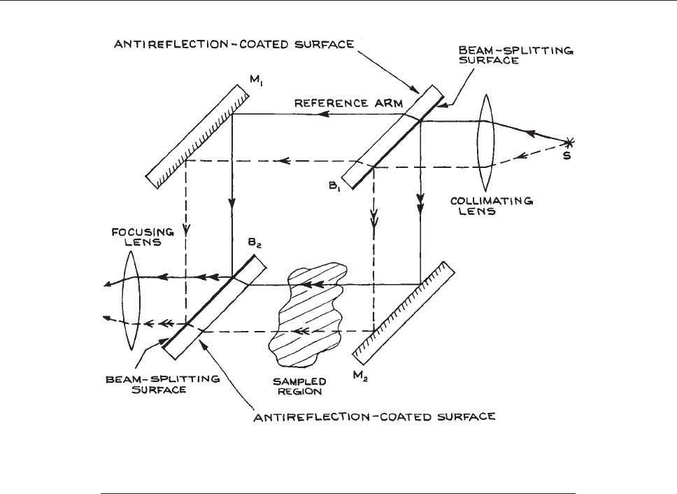
For example they might use a hot ceramic (globar type)
source for infrared work, and germanium, InGaAs,
HgCdTe, or triglycine sulfate (TGS) detectors, depending
on the spectral region of interest.
The Mach–Zehnder Interferometer. The Mach–
Zehnder interferomete r, shown in Figure 4.170,iswidely
used
for studying refra ctive-index distributions in gases,
liquids, and solids. It is particularly widely used for
studying the density variations in compressible gas
flows,
151
the thermally i nduced density (and consequent
refractive-index) changes behind shock fronts, and
thermally induced density changes produced by la ser
beams propagating through transparent media.
152,153
If the light entering the interferometer is perfectly
collimated, uniform output illumination results, which
is a maximum if the path difference between the two
arms is an integral number of wavelengths. If the image
of M
1
in beamsplitter B
2
is not parallel to M
2
, the ou tput
fringe pattern is essentially the interference pattern
observed from a wedge – a series of parallel bright and
dark bands. If the medium in arm 2 is perturbed i n
some way, so that a spatial variation in refractive index
results, the output fringe pattern changes. Analysis of
the new fringe pattern reveals the spatial distribution
of refractive-index variation al ong the beam path in
arm 2. Various design variations on the Mach–Zehnder
interferometer exist, notably the Jamin and the Sirks–
Pringsheim.
11,154
Figure 4.170 Mach-Zehnder interferometer. M
1
,M
2
are totally reflecting mirrors;
B
1
,B
2
are beamsplitters (usually equally reflective and transmissive). The
distribution of output illumination reflects the refractive-index distribution in
the sampled region.
OPTICAL DISPERSING INSTRUMENTS 313

Design Considerations for Double-Beam
Interferometers.
Michelson and Mach–Zehnder inter-
ferometers are much easier to build in the laboratory than
multiple-beam interferometers, such as the Fabry–Perot.
Because the beams only reflect off the interfero-
meter mirrors once, mirrors of flatness k/10 or k/20 are quite
adequate for building a good instrument. The usual precau-
tions should be taken in construction: stable rigid mounts for
the mirrors and beamsplitters and, if long-term thermal
stability is required, low-expansion materials. Piezoelectric
control of mirror alignment is not generally necessary, as
these instruments are less sensitive to small angular mis-
alignments than Fabry–Perot interferometers. To achieve
freedom from alignment disturbances along one or two
orthogonal axes, the plane mirrors of a Michelson interfer-
ometer can be replaced with right-angle prisms or corner-
cube retroreflectors, respectively. Some care should be taken
to avoid source-polarization effects in these instruments; the
beamsplitters are generally designed to reflect and transmit
equal amounts only for a specific input polarization. If
polarizing materials are placed in either arm of the interfer-
ometer, no fringes will be seen if, by any chance, the beams
from the two arms emerge orthogonally polarized.
Endnotes
a 1 GHz (GigaHertz) ¼10
9
Hz, 1 THz (TeraHertz)
¼10
12
. The infrared range can also be somewhat
arbitrily divided up into the submillimeter region
(k ¼0.1–1 mm), far-infrared (k ¼20–100 lm), middle
infrared (k ¼3–20 lm), and the near infrared (k ¼0. 7 –
3 lm).
b At the boundary separating one or more anisotropic
media, Snell’s law must be used with some care as,
in anisotropic media, the ray direction is not in general
parallel to the wave vector (or wave normal), which is
also used to characterize the direction of the ray.
15
c Used by physicians for examining the retina of a
patient’s eye.
17
d A pinhole camera is free of all aberrations in a geomet-
rical optics description.
e A simple lens with just two spherical surfaces.
f Often called a TM wave.
g Often called a TE wave
h The old pressure unit of pounds per square inch (psi) ¼
6895 Pa
i The word rugate means corrugated, having alternating
ridges and depressions
j The phosphorous is often omitted, and the precise stoi-
chiometry of (In, Ga) and (As, P) determines the laser
wavelength
k In practice, in any real system, transmission losses and
aberrations will cause B
2
< B
1
Cited References
1. Proceedings of the Symposium on Quasi-Optics, New York,
June 8–10, 1964, J. Fox (Ed.), Polytechnic Press of the
Polytechnic Institute of Brooklyn, New York, 1964.
2. Pr oceedings of the Symposium on Submillimeter Waves,New
York, March 31–April 2, 1970, J. Fox (Ed.), Polytechnic Press
of the Polytechnic Institute of Brooklyn, Ne w York, 1964.
3. A. Mortazawi, T. Itoh, and J. Harvey, Active Antennas and
Quasi-Optical Arrays, Wiley-IEEE Press, New York, 1998.
4. J. Lesurf, Millimeter-Wave Optics, Devices and Systems,
Lavoisier, Chachan, 1990.
5. K. M. Baird, D. S. Smith, and B. G. Whitford, Confirmation
of the currently accepted value 299792458 metres per second
for the speed of light, Opt. Commun., 31,367–368,1979.
6. E. R. Cohen and B. N. Taylor, Committee on Data
for Science and Technology , CODATA Bulletin,No.63, 1986.
7. G. W. C. Kaye and T. H. Laby, Tables of Physical and
Chemical Constants, 16th edn., Longman, London: 1995.
Now available free online at http://www.kayelaby.npl.
co.uk/
8. C. D. Coleman, W. R. Bozman, and W. F. Meggers, Table of
Wavenumbers, US Nat’l. Bur. Std. Monograph 3, Vols. 1–2,
1960.
9. M. W. Urban, Attenuated Total Reflectance Spectroscopy
of Polymers: Theory and Practice, American Chemical
Society, Washington, DC, 1996.
10. R. Wies endanger, Scanning Probe Microsocopy and
Spectroscopy, Cambridge Uni versity Press, Cambridge, 1994.
11. M. Born and E. Wolf, Principles of Optics, 7th ed.,
Cambridge University Press, Cambridge, 1999.
12. E. E. Wahlstrom, Optical Crystallography, 5th edn., John
Wiley & Sons, Inc., New York, 1979.
13. W. A. Shurcliff, Polarized Light: Production and Use,
Harvard University Press, Cambridge, MA, 1962.
14. A. Yariv, Optical Electronics in Modern Communications,
5th edn., Oxford University Press, New York, 1997.
314 OPTICAL SYSTEMS

15. C. C. Davis, Lasers and Electro-Optics, Cambridge
University Press, Cambridge, 1996.
16. H. Kogelnik and T. Li, Proc. IEEE, 54, 1312–1329, 1966.
17. R. Kingslake, Optical System Design, Academic Press,
Orlando, FL, 1983.
18. Code V. Available from Optical Research Associates.
19. Zemax. Available from Zemax Development
Corporation.
20. Oslo developed by Sinclair Optics, Inc. Distributed by
Lambda Research Corporation.
21. Solstis Odyssey. Available from Optis.
22. Optikwerk. Available from Optikwerk, Inc.
23. R. W. Ditchburn, Light, 3rd edn., Academic Press,
New York, 1976.
24. L. Levi, Applied Optics, Vol.1 John Wiley & Sons, Inc.,
New York, 1968.
25. W. J. Smith, Modern Optical Engineering, 3rd edn., SPIE
Press, Bellingham, WA, 2000.
26. W. J. Smith, Modern Lens Design: A Resource Manual,
McGraw-Hill, New York, 1992.
27. R. R. Shannon, The Art and Science of Optical Design,
Cambridge University Press, Cambridge, 1997.
28. M. Laikin, Lens Design, 3rd edn., Marcel Dekker, New
York, 2001.
29. S. Ramo, J. R. Whinnery, and T. Van Duzer, Fields and
Waves in Communication Electronics, 3rd edn., John
Wiley & Sons, Inc., New York, 1994.
30. Diffraction-limited spherical lenses are available from
Melles Griot, Optics for Research, Newport, Special
Optics, and J. L. Wood Optical Systems, among others (see
following reference).
31. Laser Focus Buyers Guide, published annually by
Pennwell Publishing Co., 1421 South Sheridan, Tulsa, OK
74112 01460, lists a large number of suppliers of a wide
range of optical components and systems as does the
The Photonics Buyers’ Guide, published annually by
Photonics Spectra, Laurin Publishing Co., Berkshire
Common, P. O. Box 4949, Pittsfield, MA 01202-4949.
Additional valuable listings of this sort are: Lasers and
Optronics Buying Guide, published a nnually by Cahners,
301 Gibral tar Drive, Box 650, Morris Plains,
NJ 07950-0650; and Lightwave, 98 Spit Brook Road,
Suite 100, Nashua, NH 03062–5737.
32. The ‘‘float’’ method for manufacturing plate glass
(developed by Pilkington Glass) involves the drawing of the
molten glass from a furnace, where the molten glass floats on
the surface of liquid tin. The naturally flat surface of the
liquid metal ensures the production of much larger sheets of
better-flatness glass than was possible by earlier techniques.
33. Alexander Hornberg (Ed.), Handbook of Machine Vision,
John Wiley & Sons, Inc., New York, 2006.
34. G. Rempe, R. J. Thompson, H. J. Kimble, and R. Lalezari,
Opt. Lett., 17, 363–365, 1992.
35. C. J. Hood, H. J. Kimble, and J. Ye, Phys. Rev. A, 64,033804,
2001.
36. H. R. Bilger, P. V. Wells, and G. E. Stedman, Appl. Opt., 33,
7390–7396, 1994.
37. H.-J. Cho, M.-J. Shin, and J.-C. Lee, Appl. Opt. 45, 1440–
1446, 2006.
38. A. B. Meinel, in Applied Optics and Optical Engineering,
Vol. 5, R. Kingslake (Ed.), Academic Press, New York,
1969.
39.
W. Brouwer and A. Walther, Design of optical instruments,
in Advanced Optical Techniques, A. C. S. Van Heel, (Ed.),
North-Bouand, Amsterdam, 1967.
40. Celestron Telescopes are available from Celestron
International, 2835 Columbia Street, P.O. Box 3578,
Torrance, CA 90503; (310) 328–9560.
41. Meade Telescopes are available from Meade Instruments
Corporation, 6001 Oak Canyon, Irvine, California
92618–5200, (949) 451–1450.
42. W. T. Wellford and R. Winston, High Collection Nonimaging
Optics, Academic Press, San Diego, CA, 1989.
43. R. Winston, J. C. Min
˜
ano, and P. G. Benitez, Nonimaging
Optics, Elsevier, Amsterdam, 2005.
44. A. Girard and P. Jacquinot, in Advanced Optical
Techniques,A.C.S.VanHeel(Ed.),North-Bouand,
Amsterdam, 1967.
45. J. D. Strong, Procedures in Experimental Physics,
Prentice-Hall, Englewood Cliffs, NJ, 1938.
46. David R. Lide (Ed.), Handbook of Chemistry and Physics,
81st. edn., CRC Press, Boca Raton, FL, 2000.
47. D. R. Goff, Fiber Optic Reference Guide, 3rd edn., Focal
Press (Elsevier), Amsterdam, 2002.
48. U. Hochuli and P. Haldemann, Rev. Sci. Instr., 43, 1088–
1089, 1972.
49. Epoxy-removing solvents are available from Electron
Microscopy Services, Oakite, or Hydroclean.
50. T. C. Poulter, Phys. Rev., 35,297,1930.
51. W. Paul, W. W. Meis, and J. M. Besson, Rev. Sci. Instr., 39,
928–930, 1968.
52. I. L. Spain and J. Paawe (Eds.), High Pressure Technology,
Dekker, New York, 1967.
53. Compilation of ASTM Standard Definitions, 3rd edn.,
American Society for Testing and Materials, Philadelphia,
1976.
REFERENCES 315

54. Glass, quartz, and sapphire vacuum window assembles are
available from Adolf Meller, Ceramaseal, Varian, and
Vacuum Generators.
55. D. H. Martin (Ed.), Spectroscopic Techniques for Far
Infra-Red, Submillimetre and Millimetre Waves,
NorthHolland, Amsterdam, 1967.
56. K. D. Moller and W. G. Rothschild, Far-Infrared
Spectroscopy, Wiley-Interscience, New York, 1971.
57. A. Hadni, Essentials of Modern Physics Applied to the
Study of the Infrared, Pergamon Press, Oxford, 1967.
58. G. A. Fry, Applied Optics and Optical Engineering, Vol. 2,
R. Kingslake (Ed.), Academic Press, 1965.
59. C. C. Davis and R. A. McFarlane, J. Quant. Spect. Rad.
Trans., 18, 151–170, 1977.
60. P. W. Kruse, L. D. McGlauchlin, and R. B. McQuistan,
Elements of Infrared Technology: Generation,
Transmission and Detection, John Wiley & Sons, Inc.,
New York, 1962.
61. R. D. Hudson, Jr., Infrared System Engineering,
Wiley-Interscience, New York, 1969.
62. J. A. R. Samson, Techniques of Vacuum Ultraviolet
Spectroscopy, John Wiley & Sons, Inc., New York, 1967.
63. Available from EG&G Optoelectronics, ILC, Verre &
Quartz, and Xenon Corporation.
64. Available from EG&G Optoelectroncs, Verre & Quartz,
Resonance, and Xenon Corporation.
65. J. P. Markiewicz and J. L. Emmett, IEEE J. Quant. Elec-
tron., QE-2, 707–711, 1966.
66. J. G. Edwards, Appl. Opt., 6, 837–843, 1967.
67. H. J. Baker and T. A. King, J. Phys. E.: Sci. Instr., 8, 219–
223, 1975.
68. William T. Silfvast, Laser Fundamentals, 2nd edn.,
Cambridge University Press, Cambridge, 2004.
69. B. E. A. Saleh and M. C. Teich, Fundamentals of Photonics,
John Wiley & Sons, Inc., New York, 1991.
70. A. E. Siegman, Lasers, University Science Books, Mill
Valley, CA, 1986.
71. H. Rabin and C. L. Tang (Eds.), Quantum Electronics, Vols.
1A and 2A, Nonlinear Optics, Academic Press, New York,
1975.
72. Nonlinear Optics, Proceedings of the Sixteenth Scottish
Universities Summer School in Physics, 1975, P. G. Harper
and B. S. Wherrett (Eds.), Academic Press, London, 1977.
73. N. Bloembergen, Nonlinear Optics, Benjamin, New York,
1965.
74. F. Zernike and J. E. Midwinter, Applied Nonlinear Optics,
John Wiley & Sons, Inc., New York, 1973.
75. R. W. Boyd, Nonlinear Optics, Academic Press,
Boston, 1992.
76. D. Ro
¨
ss, Lasers, Light Amplifiers and Oscillators,
Academic Press, New York, 1969.
77. W. Koechner, Solid
State Laser Engineering, 5th revised
and updated edn., Springer-Verlag, Berlin, 1999.
78. F. P. Scha
¨
fer (Ed.), Topics in Applied Physics, Vol. 1, Dye
Lasers, 3rd revised and enlarged edn., Springer-Verlag,
Berlin, 1990.
79. H. W. Furumoto and H. L. Ceccon, Appl. Opt., 8, 1613–
1623, 1969.
80. J. F. Holzrichter and A. L. Schawlow, Ann. N.Y. Acad. Sci.,
168, 703–714, 1970.
81. T. B. Lucatorto, T. J. McIlrath, S. Mayo, and H. W.
Furumoto, Appl. Opt., 19, 3178–3180, 1980.
82. C. C. Davis and T. A. King, Advances in Quantum Elec-
tronics, Vol. 3, D. W. Goodwin (Ed.), Academic Press,
London, 1975, pp. 169–454.
83. W. B. Bridges, Handbook of Laser Science and Technology,
Vol. 1: Lasers in All Media, M. J. Weber (Ed.), CRC Press,
Boca Raton, FL, 1982.
84. C. C. Davis, Handbook of Lasers Science and Technology,
Vol. 1, Lasers in All Media, M. J. Weber (Ed.), CRC Press,
Boca Raton, FL, 1982.
85. D. C. Tyte, Advances in Quantum Electronics, Vol. 1, D. W.
Goodwin (Ed.), Academic Press, London, 1970.
86. J. J. Degnan, Appl. Phys., 11, 1–33, 1976.
87. H. Seguin and J. Tulip, Appl. Phys. Lett., 21, 414–415,
1972.
88. J. D. Cobine, Gaseous Conductors, Dover, New York, 1958.
89. H. J. Seguin, K. Manes, and J. Tulip, Rev. Sci. Instr., 43,
1134–1139, 1972.
90. A. J. Beaulieu, Appl. Phys. Lett., 16, 504–505, 1970.
91. D. Basting, F. P. Scha
¨
fer, and B. Steyer, Opto-electron., 4,
43–49, 1972.
92. P. Schenck and H. Metcalf, Appl. Opt., 12, 183–186, 1973.
93. C. P. Wang, Rev. Sci. Instr., 47, 92–95, 1976.
94. A. J. Schwab and F. W. Bouinger, IEEE J. Quant,. Elec-
tron., QE-12
, 183–188, 1976.
95.
C. L. Sam, Appl. Phys. Lett., 29, 505–506, 1976.
96. M. Feldman, P. Lebow, F. Raab, and H. Metcalf, Appl. Opt.,
17, 774–777, 1978.
97. M. J. F. Digonnet (Ed.), Rare Earth Doped Fiber Lasers
And Amplifiers, 2nd Revised edn., Taylor & Francis Ltd.,
Abingdon, 2001.
98. L. F. Mollenauer, Opt. Lett., 1, 164, 1977 (see also Opt.
Lett. 3, 48–50, 1978; 4, 247–299, 1979; 5, 188–190,
1980).
99. R. C. Greenhow and A. J. Schmidt, Advances in Quantum
Electronics, Vol. 2, D. W. Goodwin (Ed.), Academic Press,
London, 1973.
316 OPTICAL SYSTEMS

100. S. L. Shapiro (Ed.), Ultrashort Light Pulses, Picosecond
Techniques and Applications, Topics in Applied Physics,
Vol. 18, Springer, Berlin, 1977.
101. C. H. Lee (Ed.), Picosecond Optoelectronic Devices,
Academic Press, Orlando, FL, 1984.
102. P. Bhattacharya, Semiconductor Optoelectronic Devi-
ces, 2nd edn., Prentice-Hall, Upper Saddle River, NJ,
1997.
103. J. Gowar, Optical Communication Systems, 2nd edn.,
Prentice-Hall, Englewood Cliffs, NJ, 1993.
104. D. Wood, Optoelectronic Semiconductor Devices,
Prentice-Hall, New York, 1994.
105. G. P. Agrawal and N. K. Dutta, Long-Wavelength
Semiconductor Lasers, Van Nostrand Reinhold,
New York, 1986.
106. G. H. B. Thompson, Physics of Semiconductor Laser
Devices, John Wiley & Sons, Ltd, Chichester, 1980.
107. S. L. Chuang, Physics of Optoelectronic Devices, John
Wiley & Sons, Inc., New York, 1995.
108. J. Singh, Semiconductor Optoelectronics, McGraw-Hill,
New York, 1995.
109. H. Kressel (Ed.), Semiconductor Devices for Optical
Communication, Vol. 39, Topics in Applied Physics, 2nd
updated edn., Springer-Verlag, Berlin, 1982.
110. E. Kapon (Ed.), Semiconductor Lasers, Vols. 1 and 2,
Academic Press, San Diego, CA, 1999.
111. E. D. Hinkley, K. W. Nill, and F. A. Blum, Topics in
Applied Physics, Vol. 2, H. Walther (Ed.), Springer, Ber-
lin, 1976, pp. 125–196.
112. J. Faist, F. Capasso, D. L. Sivco, et al., Science, 264
(5158), 553–556, 1994.
113. T. J. Kane and R. L. Byer, Optics Lett., 10, 65–67, 1985.
114. T. W. Ha
¨
nsch, Appl. Opt., 11, 895–898, 1972.
115. R. Wallenstein and T. W. Ha
¨
nsch, Appl. Opt., 13, 1625–
1628, 1974.
116. R. Wallenstein and T. W. Ha
¨
nsch, Opt. Commun., 14, 353–
357, 1975.
117. G. L. Eesley and M. D. Levenson, IEEE J. Quant. Elec-
tron. QE-12, 440–442, 1976.
118. M. G. Littman and H. J. Metcalf, Appl. Opt., 17, 2224–
2227, 1978.
119. M. Littman and J. Montgomery, Laser Focus/Electro-
optics,
24,
70–86, 1988.
120. M. B. Radunsky, Laser Focus World, p. 107, October
1995.
121. B. J. Orr et al., Tunable Laser Applications, F. J. Duarte
(Ed.), Marcel Dekker, New York, 1995.
122. R. G. Batchko, D. R. Weise, T. Plettner, et al., Opt. Lett.
23(3), 168, 1998.
123. M. E. Klein, D.-H. Lee, J.-P. Meyn, K.-J. Boller, and
R. Wallenstein, Opt. Lett., 24, 1142–1144, 1999.
124. F. Mu
¨
ller, G. von Basum, A. Popp, et al., Appl. Phys. 80,
307–313, 2004.
125. I. P. Kaminow, An Introduction to Electro-optic Devices,
Academic Press, New York, 1974.
126. A. Korpel, Acousto-Optics, Marcel Dekker, New York,
1988, see also Acousto-Optics – a review of fundamentals,
Proc. IEEE., 69, 48–53, 1981.
127. I. C. Chang, IEEE Trans. Sonics and Ultrasonics, SU-23,
2–22, 1976.
128. American National Standard for Safe Use of Lasers,
ANSI Z136-2-2000, Published by the Laser Institute of
America, Suite 128, 13501 Ingenuity Drive, Orlando, FL
32826.
129. D. Sliney and M. Wolbarsht, Safety with Lasers and Other
Optical Sources: A Comprehensive Handbook, Plenum,
New York, 1980.
130. M. J. Weber (Ed.), CRC Handbook of Laser Science and
Technology, Vol. 1, Lasers and Masers, CRC Press, Boca
Raton, FL, 1982.
131. P. Jacquinot, J. Opt. Soc. Am., 44, 761–765, 1954.
132. R. Kingslake (Ed.), Applied Optics and Optical Engi-
neering, Vol. 5: Optical Instruments Part II, Academic
Press, New York, 1969.
133. J. F. James and R. S. Sternberg, The Design of Optical
Spectrometers, Chapman and Hall, London, 1969.
134. The Photonics Design and Applications Handbook,
published annually by Laurin Publishing Co. Inc.,
Pittsfield, MA.
135. W. G. Fastie, J. Opt. Soc. Am., 42, 641–647, 1952.
136. H. Ebert, Annalen der Physik und Chemie, 38, 489–493,
1889.
137. M. Seya, Sci. Light (Tokyo), 2, 8–17, 1952.
138. T. Namioka, Sci. Light (Tokyo),
3,
15–24, 1952.
139. P. Atherton, N. Reay, J. Ring, and T. Hicks, Opt. Eng., 20,
806, 1981.
140. Available from numerous suppliers of vacuum equipment –
for example, Ceram Tec (Ceramaseal Division), Edwards,
Ferrofluidics Corp., Perkin Elmer, Vacuum Generators
(VG), Varian, and Veeco.
141. Available from Carpenter Technology, P.O. Box 14662,
Reading, PA 19612–4662; Tel: (800) 338–4592 and (610)
208–2000, FAX: (610) 208–2361.
142. Available from Burleigh.
143. Available from Heraeus-Amersil, Dynasil, Esco, and
Quartz Scientific, among others.
144. Available from Corning Glass Works, Optical Products
Department.
REFERENCES 317

145. Piezoelectric transducers are available from American
Piezo Ceramics, Burleigh, EDO, Polytec, Queensgate
Instruments, and Xinetics, among others.
146. C. F. Bruce, Appl. Opt., 5, 1447–1452, 1966.
147. Commercial Fabry–Perot Interferometers that can
incorporate this feature are available from Burleigh.
148. P. Hariharan, Optical Interferometry, 2nd edn., Academic
Press, 2003.
149. B. T. Meggitt and K. T. V. Grattan, Optical Fiber Sensor
Technology, Springer, New York, 1999.
150. James C. Wyant, White light interferometry, paper
presented at AeroSense, Orlando, Florida, 1–5 April
2002. (Available online at fttp://www.optics.arizona.edu/
jcwyant/pdf/Meeting_papers/WhiteLightInterferometry.pdf)
151. R. Ladenburg and D. Bershader, High Speed Aerody-
namics and Jet Propulsion, Vol. 9, Physical Measurements
in Gas Dynamics and Combustion, R. Ladenburg (Ed.),
Princeton University Press, Princeton, NJ, 1954.
152. P. R. Longaker and M. M. Litvak, J. Appl. Phys., 40,
4033–4041, 1969.
153. D.C. Smith, IEEE J. Quant. Electron., QE-5, 600–607, 1969.
154. H. Kuhn, Rep. Prog. Phys., 14, 64–94, 1951.
General References
Comprehensive (General)
Optics Texts
M. Born and E. Wolf, Principles of Optics, 7th edn., Cambridge
University Press, Cambridge, 1999.
E. Hecht, Optics, 3rd edn., Addison-Wesley, Reading, MA, 1998.
R. W. Ditchburn, Light, 3rd edn., Academic Press, New York, 1976.
F. A. Jenkins and H. E. White, Fundamentals of Optics, 4th edn.,
McGraw-Hill, New York, 1976.
M. V. Klein and T. E. Furtak, Optics, 2nd edn., John Wiley &
Sons, Inc., New York, 1986.
R. S. Longhurst, Geometrical and Physical Optics, 3rd edn.,
Longman, London, 1973.
F. G. Smith and J. H. Thomson, Optics, 2nd edn., John Wiley &
Sons, Inc., Chichester, 1988.
J. Strong, Concepts of Classical Optics, Freeman, San Francisco,
CA, 1958.
Applied Optics
W. J. Smith, Modern Optical Engineering, 3rd edn., SPIE Press,
Bellingham, WA, 2000.
R. Kingslake (Ed.), Applied Optics and Optical Engineering
Academic, New York, Vol. 1, 1965; Vol. 2, 1965; Vol. 3, 1965;
Vol. 4, 1967; Vol. 5, 1969.
L. Levi, Applied Optics, John Wiley & Sons, Inc., New York,
Vol. 1, 1968; Vol. 2, 1980.
Lens Design
W. J. Smith, Modern Lens Design: A Resource Manual,
McGraw-Hill, New York, 1992.
R. R. Shannon, The Art and Science of Optical Design,
Cambridge University Press, Cambridge, 1997.
M. Laikin, Lens Design, 3rd edn., Marcel Dekker, New York,
2001.
Electro-Optic Devices
M. A. Karim, Electro-Optical Devices and Systems, PWS-Kent
Publishing, Boston, MA, 1990.
I. P. Kaminow, An Introduction to Electro-Optics, Academic
Press, New York, 1974.
A. Yariv, Optical Electronics in Modern Communications,
5th edn., Oxford University Press, New York, 1997.
Far-Infrared Techniques
M. F. Kimmitt, Far-Infrared Techniques, Routledge, 1970.
A. Hadni, Essentials of Modern Physics Applied to the Study
of the Infrared, Pergamon Press, Oxford, 1967.
K. D. Mo
¨
ller and W. G. Rothschild, Far-Infrared Spectroscopy,
Wiley-Interscience, New York, 1971.
L. C. Robinson, Physical Principles of Far-Infrared Radiation,
Methods in Experimental Physics, Vol. 10, L. Marton (Ed.),
Academic Press, New York, 1973.
Fiber Optics
J. Hecht, Understanding Fiber Optics, 3rd edn., Prentice-Hall,
Upper Saddle River, NJ, 1999.
A. Ghatak and K. Thyagarajan, Introduction to Fiber
Optics, Cambridge University Press, Cambridge, 1998.
A. Ghatak, A , Sharma, and R. Tewari, Understanding
FiberOpticsonaPC, Viva Books P rivate Ltd., New
Delhi, 1994. P.K. Cheo, Fiber Optics and Optoelectronics,
2nd edn., Prentice-Hall, Englewood Cliffs, NJ, 1990. L.
Kazovsky, S. Benedetto, and A. Willner, Optical Fiber
Communication Systems,ArtechHouse,Boston,MA,
1996.
318 OPTICAL SYSTEMS

J. Gowar, Optical Communication Systems, 2nd edn. Prentice-
Hall, Englewood Cliffs, NJ, 1993.
M. K. Barnoski, (Ed.,) Introduction to Integrated Optics, Plenum,
New York, 1974.
D. Marcuse, Principles of Optical Fiber Measurements,
Academic Press, San Diego, CA., 1981.
T. Okoshi, Optical Fibers, Academic Press, New York, 1982.
D. Gloge (Ed.), Optical Fiber Technology, IEEE, New York,
1976.
J. C. Palais, Fiber Optic Communications, 5th edn.,
Prentice-Hall, Upper Saddle River, NJ, 2004.
A. D. Snyder and J. D. Love, Optical Waveguide Theory,
Chapman and Hall, London and New York, 1983.
Filters
D. R. Lide (Ed.), Handbook of Chemistry and Physics, 87th
edn., Taylor and Francis, Boca Raton, Florida, 2000. Also
available on line at http://www.hbcpnetbase.com/help/
default.asp
R. J. Pressley (Ed.), Handbook of Lasers, CRC Press, Cleveland,
OH, 1971.
L. Levi, Applied Optics, Vol. 2, John Wiley & Sons, Inc., New
York, 1980.
H. A. Macleod, Thin-Film Optical Filters, American Elsevier,
New York, 1969.
E. J. Bowen, Chemical Aspects of Light, 2nd revised edn., The
Clarendon Press, Oxford, 1946.
Fourier Transform Spectroscopy
P. Griffiths and J. deHaseth, Fourier Transform Infrared
Spectroscopy, John Wiley & Sons, Inc., New York,
1986.
B. C. Smith, Fundamentals of Fourier Transform Infrared
Spectroscopy, CRC Press Inc., Boca Raton, IL, 1996.
Incoherent Light Sources
A. C. S. Van Heel (Ed.), Advanced Optical Techniques,
North-Bouand, Amsterdam, 1967.
R. Kingslake (Ed.), Applied Optics and Optical Engineering,
Vol. 1, Academic Press, New York, 1965.
R. J. Pressley (Ed.), Handbook of Lasers, CRC Press, West Palm
Beach, FL, 1971.
L. Levi, Applied Optics, Vol. 1, John Wiley & Sons, Inc., New
York, 1968.
Photometry
C. DeCusatis, Handbook of Applied Photometry, AIP Press, New
York, (1997).
M. Rea (Ed.), Lighting Handbook: Reference and Application,
8th edn., Illuminating Engineering Society of North America,
New York, 1993.
Infrared Technology
W. L. Wolfe and G. J. Zissis (Eds.), The Infrared Handbook,
Office of Naval Research, Washington, DC, 1985.
A. R. Jha, Infrared Technology, John Wiley & Sons, Inc., New
York, 2000.
A. Hadni, Essentials of Modern Physics Applied to the Study of
the Infrared, Pergamon Press, Oxford, 1967.
R. D. Hudson, Infrared System Engineering,
Wiley-Interscience, New York, 1969.
P. W. Kruse, L. D. McGlauchlin, and R. B. McQuistan, Elements
of Infrared Technology, John Wiley & Sons, Inc., New York,
1962.
Interferometers and Interferometry
P. Hariharan, Optical Interferometry, Academic Press, Orlando,
FL, 1985.
G. Hernandez, Fabry–Perot Interferometers, Cambridge
University Press, Cambridge, 1986.
R. Jones and C. Wykes, Holographic and Speckle
Interferometry, 2nd edn., Cambridge University Press,
Cambridge, 1989.
J. C. Dainty (Ed.), Laser Speckle and Related Phenomena, Topics
in Applied Physics, Vol. 9, Springer-Verlag, Berlin; New York,
1975.
M. Francon, Laser Speckle and Applications in Optics, Academic
Press, New York, 1979.
M. Born and E. Wolf, Principles of Optics, 7th edn., Cambridge
University Press, Cambridge, 1999.
M. Francon, Optical Interferometry, Academic Press, New York,
1966.
W. H. Steel, Interferometry, 2nd edn., Cambridge University
Press, Cambridge, 1983.
S. Tolansky, An Introduction to Interferometry, Longman,
London, 1955.
J. M. Vaughan, The Fabry–Perot Interferometer: History,
Theory, Practice and Applications, Adam Hilger, Bristol, UK,
1989.
REFERENCES 319

Fourier Optics and Holography
J. Goodman, Introduction to Fourier Optics, 2nd edn., McGraw-
Hill, New York, 1996.
P. Hariharan, Optical Holography, Cambridge University Press,
Cambridge, 1984.
Lasers
A. Yariv, Optical Electronics in Modern Communications, 5th
edn., Oxford University Press, New York, 1997.
C. C. Davis, Lasers and Electro-Optics, Cambridge University
Press, Cambridge, 1996.
C. R. Pollack, Fundamentals of Optoelectronics, Irwin, Chicago,
1995.
W. T. Silfvast, Laser Fundamentals, 2nd edn., Cambridge Uni-
versity Press, 2004.
B. E. A. Saleh and M. C. Teich, Fundamentals of Photonics, 2nd
edn., John Wiley & Sons, Inc., New York, 2007.
M. Weber (Ed.), Handbook of Laser Science and Technology,
Vol. 1, Lasers and Masers; Vol. II, Gas Lasers, CRC Press,
Boca Raton, FL, 1982.
A. Maitland and M. H. Dunn, Laser Physics, North
Holland, Amsterdam, 1969.
D. C. O’Shea, W. R. Callen, and W. T. Rhodes, Introduction to
Lasers and Their Applications, Addison-Wesley, Reading,
MA, 1977.
J. T. Verdeyen, Laser Electronics, 3rd edn., Prentice-Hall,
Englewood Cliffs, NJ, 1995.
A. Yariv, Quantum Electronics, 3rd edn., John Wiley & Sons,
Inc., New York, 1989.
A. E. Siegman, Lasers, University Science Books, Mill Valley,
CA, 1986.
Nonlinear Optics
R. W. Boyd, Nonlinear Optics, Academic Press, Boston, MA,
1992.
N. Bloembergen, Nonlinear Optics, Benjamin, New York, 1965.
P. G. Harper and B. S. Wherrett (Eds.), Nonlinear Optics,
Academic Press, New York, 1977.
C. L. Tang and H. Rabin, (Eds.), Quantum Electronics, Vols.
1A and 2A Nonlinear Optics, Academic Press, New York,
1975.
F. Zernike and J. E. Midwinter, Applied Non-Linear Optics, John
Wiley & Sons, Inc., New York, 1973.
Y. R. Shen, The Principles of Nonlinear Optics, John Wiley &
Sons, Inc., New York, 1984.
Optical Component and Instrument Design
A. C. S. Van Heel (Ed.), Advanced Optical Techniques,
North Holland, Amsterdam, 1967.
R. Kingslake (Ed.), Applied Optics and Optical Engineering,
Academic Press, New York, Vol. 3, 1965; Vol. 4, 1967; Vol. 5,
1969.
Optical Detectors
A. Rogalksi, Infrared Detectors, Gordon and Breadh, Amster-
dam, 2000.
J. Gowar, Optical Communication Systems, 2nd edn.,
Prentice-Hall, Englewood Cliffs, NJ, 1993.
E. L. Dereniak and G. D. Boreman, Infrared Detectors and
Systems, John Wiley & Sons, Inc., New York, 1996.
E. L. Dereniak and D. G. Crowe, Optical Radiation Detectors,
John Wiley & Sons, Inc., New York, 1984.
J. Graeme, Photodiode Amplifiers, McGraw-Hill, New York,
1996.
J. B. Dance, Photoelectronic Devices, Iliffe, London, 1969.
P. W. Kruse, L. D. McGlauchlin, and R. B. McQuistan, Elements
of Infrared Technology, John Wiley & Sons, Inc., New York,
1962.
L. Levi, Applied Optics, Vol. 2, John Wiley & Sons, Inc., New
York, 1980.
R. S. Keyes (Ed.), Optical and Infrared Detectors, Topics in
Applied Physics, Vol. 19, Springer, Berlin, 1977.
Optical Materials
R. Kingslake (Ed.), Applied Optics and Optical Engineering,
Vol. 1, Academic Press, New York, 1965.
M. Weber (Ed.), Handbook of Laser Science and Technology,
Vols. III–V, Optical Materials, CRC Press, Boca Raton, FL,
1986–87.
P. W. Kruse, L. D. McGlauchlin, and R. B. McQuistan, Elements
of Infrared Technology, John Wiley & Sons, Inc., New York,
1962.
A. J. Moses, Optical Material Properties, IFI/Plenum, New York,
1971.
Optical Safety
M. J. Weber (Ed.), Handbook of Laser Science and
Technology, Vol. 1, Lasers and Masers, CRC Press, Boca
Raton, FL, 1982.
320 OPTICAL SYSTEMS

D. Sliney and M. Wolbarsht, Safety with Lasers and Other
Optical Sources: A Comprehensive Handbook, Plenum, New
York, 1980.
Polarized Light and Crystal Optics
R. M. A. Azzam and N. M. Bashara, Ellipsometry and Polarized
Light, North-Bouand, Amsterdam, 1977.
D. Goldstein, Polarized Light, CRC Press, Boca Raton, FL, 2003.
W. A. Shurcliff, Polarized Light, Harvard University Press,
Cambridge, MA, 1962.
E. Wahlstrom, Optical Crystallography, 5th edn., John Wiley &
Sons, Inc., New York, 1979.
A. Yariv and P. Yeh, Optical Waves in Crystals,JohnWiley&Sons,
Inc., New York, 1983.
Spectrometers
N. B. Colthup, L. H. Daly, and S. E. Wiberley, Introduction to
Infrared and Raman Spectroscopy, 2nd edn., Academic Press,
New York, 1975.
Francis M. Mirabella Jr., (Ed.), Internal Reflection
Spectroscopy. Theory and Applications, CRC Press, Boca
Raton, 1993.
J. F. James and R. S. Sternberg, The Design of Optical
Spectrometers, Chapman & Hall, London, 1969.
H. S. Strobel and W. R. Heineman, Chemical Instrumentation,
3rd edn., John Wiley & Sons, Inc., New York, 1989.
Spectroscopy
M. Pinta (Ed.), Atomic Absorption Spectrometry, John Wiley &
Sons, Inc., New York, 1975.
J. R. Edisbury, Practical Hints on Absorption Spectrometry,
Hilger and Watts, London, 1966.
R. J. Reynolds and K. Aldous, Atomic Absorption Spectroscopy,
Barnes and Noble, New York, 1970.
A. Lee Smith, Applied Infrared Spectroscopy: Fundamentals,
Techniques and Analytical Problem-Solving, Vol. 54
(Chemical Analysis, Vol. 21), John Wiley & Sons, Inc.,
New York, 1979.
R. A. Sawyer, Experimental Spectroscopy, Prentice-Hall,
Englewood Cliffs, NJ, 1951.
D. Williams (Ed.), Methods of Experimental Physics, Vol. 13,
Spectroscopy, Parts A and B, Academic Press, New York,
1968.
S. Walker and H. Straw, Spectroscopy, Vol. I, Microwave and
Radio Frequency Spectroscopy; Vol. II, Ultraviolet, Visible,
Infrared and Raman Spectroscopy, Macmillan, New York,
1962.
Submillimeter Wave Techniques
K. J. Button, Infrared and Millimeter Waves:
Submillimeter Techniques, Academic Press, New York,
1980.
G. W. Chantry, Submillimeter Spectroscopy, Academic Press,
New York, 1971.
E. Kollberg (Ed.), Instrumentation for submillimeter
spectroscopy, SPIE Proceedings, Vol. 598, SPIE, Bellingham,
WA, 1986.
D. H. Martin (Ed.), Spectroscopic Techniques, North-Holland,
Amsterdam, 1967.
Tables of Physical and Chemical Constants
G. W. C. Kaye and T. H. Laby, Tables of Physical and Chemical
Constants, 16th edn., Longman, London, 1995. Now available
free online at http://www.kayelaby.npl.co.uk/
Tables of Spectral and Laser Lines
M. J. Weber, Handbook of Lasers, CRC Press, Boca Raton, FL,
2001.
M. J. Weber, Handbook of Laser Wavelengths, CRC Press, Boca
Raton, FL, 1999.
G. R. Harrison, MIT Wavelength Tables, MIT Press, Cambridge,
MA, 1969.
A. R. Striganov and N. S. Sventitskii, Tables of Spectral Lines
of Neutral and Ionized Atoms, IFI/Plenum, New York,
1968.
A. N. Zaidel’, V. K. Prokof’ev, S. M. Raiskii, V. A. Slavnyi, and
E. Ya. Shreider, Tables of Spectral Lines, IFI/Plenum, New
York, 1970.
Ultraviolet and Vacuum-Ultraviolet
Technology
A. E. S. Green (Ed.), The Middle Ultraviolet: Its Science
and Technology, John Wiley & Sons, Inc., New York, 1966.
J. A. R. Samson, Techniques of Vacuum Ultraviolet Spectroscopy,
John Wiley & Sons, Inc., New York, 1967.
REFERENCES 321

Suppliers of Optical Windows
Several of the suppliers listed will supply lenses, prisms, and
other components fabricated from these materials:
AMTIR (GeAsSe Glass): Harrick Scientific, Janos, REFLEX
Analytical
Arsenic trisulfide: Infrared Optical Products, REFLEX
Analytical, Spectrum Thin Films Corp.
Arsenic triselenide: Infrared Optical Products, REFLEX
Analytical, Spectrum Thin Films Corp.
Barium fluoride: Crystran, Del Mar Photonics, Harrick Scientific,
Infrared Optical Products, ISP Optics, Janos, Koch Crystal
Finishing, Molecular Technology.
Cadmium sulfide: Cleveland Crystals, Molecular Technology.
Cadmium selenide: Cleveland Crystals, Molecular Technology.
Cadmium telluride (Irtran 6): Cleveland Crystals, ISP Optics,
Janos, Laser Research Optics, Molecular Technology.
Calcium carbonate (calcite): Crystran, Karl Lambrecht Corp
(KLC), Photox, Thin Film Lab.
Calcium fluoride (Irtran 3): Argus International, Coherent, Inc.,
Crystran, Edmund Optics, EKSPLA, Gooch and Housego,
Hellma International, Infrared Optical Products, ISP Optics,
Janos, KLC, Koch Crystal Finishing, Lambda Research
Optics, Meller Optics, Molecular Technology, Newport,
Optimax, Opto-Sigma, Photox, REFLEX Analytical, Rocky
Mountain Instruments, Spectrum Thin Films, Thorlabs.
Cesium bromide: Argus International, Crystran, Harrick
Scientific, Janos.
Cesium iodide: Crystran, Koch Crystal Finishing, Molecular
Technology, REFLEX Analytical.
Diamond: Argus International, Gist Optics, Coherent
Photonics Group, II-VI Infrared, ISP Optics, Laser Power
Optics, REFLEX Analytical, Optics for Research,
Newport/Oriel.
Gallium arsenide: Argus International, Crystran, Infrared Optical
Products, II-VI Infrared, ISP Optics, Lambda Research Optics,
Laser Power Optics, Laser Research Optics, Meller Optics,
REFLEX Analytical, Rocky Mountain Instruments, Sterling
Precision Optics.
Germanium: Argus International, Coherent, Inc., Crystran,
Edmund Optics, Gooch and Housego, II-VI Infrared, ISP
Optics, Janos, Laser Power Optics, Laser Research Optics,
Meller Optics, Photox, REFLEX Analytical, Rocky Mountain
Instruments, Spectrogon, Spectrum Thin Films Corporation,
Sterling Precision Optics, Unicore.
Glasses: Coherent, Ealing, Edmund Optics, Newport,
Opto-Sigma, Rocky Mountain Instruments, Rolyn, Schott,
Sterling Precision Optics, Thorlabs.
Lithium fluoride: Argus International, Crystran, Coherent, Inc.,
EKSPLA, Hellma International, Infrared Optical Products, ISP
Optics, Lambda Research Optics, Macrooptica, Molecular
Technology, OPCO, Photox, REFLEX Analytical, Rocky
Mountain Instrument Co., Sterling Precision Optics.
Magnesium fluoride (Irtran 1): Argus International, Coherent,
Inc., Crystran, Edmund Optics, EKSPLA, Gooch and
Housego, Hellma International, Infrared Optical Products, ISP
Optics, KLC, Lambda Research Optics, Macrooptica, Meller
Optics, Molecular Technology, Newport, Optimax, Photox,
REFLEX Analytical, Rocky Mountain Instruments, Sterling
Precision Optics.
Magnesium oxide (Irtran 5): Crystran, Harrick Scientific.
Potassium bromide: Argus International, Crystran, EKSPLA,
Hilger Crystals, Infrared Optical products, ISP Optics, Janos,
Koch Crystal Finishing, Lambda Research Optics,
Macrooptica, Molecular Technology, OPCO, Photox,
REFLEX Analytical Corp., Spectrum Thin Films Corp.,
Thorlabs.
Potassium chloride: Crystran, ISP Optics, Janos, Koch Crystal
Finishing, Macrooptica, Molecular Technology, Optovac,
Photox.
Potassium iodide: Crystran.
Quartz (crystalline): Crystran, Esco, Infrared Optical Products,
ISP Optics, Janos, Meller Optics, Molecular Technology,
Newport, Opto-Sigma, Photox, REFLEX Analytical, Sterling
Precision Optics, Continental Optical, Optics for Research,
Newport/Oriel, Adolf Meller.
Sapphire: Crystran, Infrared Optical Products, ISP Optics, Laser
Power Optics, Meller Optics, Newport, Opto-Sigma, REFLEX
Analytical, Rocky Mountain Instruments, Rolyn, Sterling
Precision Optics.
Silica (fused): Esco, ISP Optics, Janos, Macrooptica, Meller
Optics, Newport, Opto-Sigma, Photox, REFLEX Analytical,
Rolyn, Schott, Sterling Precision Optics, Thorlabs, Continental
Optical, Optical Coating Lab (OCLI).
Silicon: Crystran, Infrared Optical Products, ISP Optics, Janos,
Laser Power Optics, Macrooptica, Meller Optics, Molecular
Technology, Photox, REFLEX Analytical, Rocky Mountain
Instruments, Sterling Precision Optics.
Silver bromide: Crystran, Harrick Scientific, ISP Optics,
REFLEX Analytical.
Silver chloride: Crystran, Harrick Scientific, ISP Optics,
REFLEX Analytical.
Sodium chloride: Crystran, ISP Optics, Koch Crystal Finishing,
Macrooptica, Molecular Technology, Photox.
Sodium fluoride: Crystran.
Strontium fluoride: Crystran, Harrick Scientific.
322 OPTICAL SYSTEMS

Strontium titanate: Commercial Crystal Labs, Harrick Scientific,
Hibshman-Pacific Optical, Photox.
Tellurium: Molecular Technology.
Thallium bromide: Crystran, Korth Kristalle GmbH.
Thallium bromoiodide (KRS-5): Argus International, Crystran,
Infrared Optical Products, ISP Optics, Janos, Koch Crystal
Finishing, Macrooptica, Molecular Technology, Perkin-Elmer.
Thallium chlorobromide (KRS-6): Crystran, Macrooptica,
Molecular Technology.
Titanium dioxide (rutile): Commercial Crystal Labs, Crystran,
Harrick Scientific, ISP Optics, Molecular Technology, Thin
Film Lab.
Zinc selenide (Irtran 4): Argus International, Coherent, Inc.,
Crystran, CVI Laser, Edmund Optics, EKSPLA, Gooch and
Housego, Harrick Scientific, Hellma International, II-VI
Infrared, Infrared Optical Products, ISP Optics, Janos, Laser
Power Optics, Laser Research Optics, Meller Optics, Molec-
ular Technology, REFLEX Analytical, Rocky Mountain
Instruments, Sterling Precision Optics.
Zinc sulfide (Irtran 2): Crystran, Gooch a nd Housego, Infrared
Optical Products, Laser Power Optics, Laser Resea rch
Optics, Meller, OPCO, Optimax, REFLEX Analytical,
Rocky Mountain Instruments, Sterling Precision Optics,
Zirconium dioxide: Insaco.
REFERENCES 323

CHARGED-PARTICLE OPTICS
*
Fifty years ago devices employing charged-particle beams
were confined to the purview of a small group of physicists
studying elementary processes. Today chemists, biologists,
and engineers employ beams of ions or electrons to probe
various materials and to investigate discrete processes.
Physicists are constructing beam machines to control the
momentum of interacting particles with energies from a
few tenths of an electron volt to trillions of electron volts.
Chemists routinely use mass spectrometers as analytical
tools and various electron spectrometers to probe molecular
structures. The electron microscope is one of the primary
tools of the modern biologist. Furthermore charged-
particle beam technology has spread to industry, where
electron-beam machines are used for cleaning surfaces
and welding, and ion-beam devices are used in the prepa-
ration of semiconductors.
The propertie s of c harged-par ticle beams are analo-
gous in many respe ct s to those of pho ton beams: hence
the a ppellation charged-pa r ticle optics. In the following
sections the laws of geometrical optics wi ll be covered
insofar as they apply to charged-partic le beams. The c on-
sequences of the coulombic i nteraction of charged par-
ticles will be considered. In addition we shall discuss the
design of electron and ion sources, as well as the design
of electrodes that constitute optical elements for manip-
ulating beams of charged part icles. We shall consider
primarily electrostatic focusing by elements of cylindri-
cal symmetry and restr ict discussion to particles of suffi-
ciently low kinetic energies that relativistic effects can be
ignored.
A number of excellent books and review articles are
available to the reader who wishes to pursue the topic of
electron and ion optics in greater detail.
1–6
5.1 BASIC CONCEPTS OF
CHARGED-PARTICLE OPTICS
5.1.1 Brightness
The brightness, b, of a point on a luminous object is deter-
mined by the differential of current dI that passes through
an increment of area dA about the point and shines into a
solid angle dX:
b ¼
dI
dAdX
ðlAcm
2
sr
1
Þ: ð5:1Þ
In electron or ion optics, a luminous object is usually
defined by an aperture, called a window, which is uni-
formly illuminated from one side by a stream of charged
particles. A second aperture called a pupil limits the angu-
lar spread of particles emanating from the window. This
situation, in the xz plane, is illustrated in Figure 5.1. It will
be
assumed that the system is cylindrically symmetric
about the z-axis and the distance between the window
and pupil is sufficiently great that the angular spread of
rays emanating from each point on the object is the same.
*
The science of charged-particle optics owes a great deal to the princi-
ples of design formulated by C. E. Kuyatt (1930–1998). The authors are
indebted to Dr. Kuyatt for his advice and for permission to present parts
of his ‘‘Electron Optics Lectures’’ in this chapter.
324
CHAPTER
5
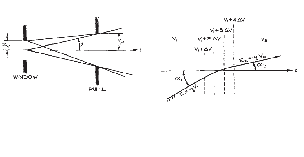
Then the integrated brightness of the object outlined by the
window is
b ¼
I
p
2
x
2
w
h
2
ð5:2Þ
where x
w
is the radius of the window and h is the half angle
defined by the pupil relative to a point at the window.
5.1.2 Snell’s Law
When a beam of charged particles enters an electric field,
the particles will be accelerated or decelerated; the trajec-
tory will depend on the angle of incidence upon the equi-
potential surfaces of the field. This effect is analogous to
the situation in optics when a light ray passes through a
medium in which there is a change of refractive index.
Figure 5.2 illustrates the behavior of a charged-particle
beam
as it passes from a region of uniform potential V
1
to a region of uniform potential V
2
. The initial and final
kinetic energies of a particle of charge q that originates at
ground potential with no kinetic energy are E
1
¼qV
1
and
E
2
¼qV
2
, respectively (i.e., for V in volts and E in eV, the
charge q on an electron is 1, and the charge of a singly
charged positive ion is +1). a
1
and a
2
are the angles of
incidence and refraction with respect to the normals to
the equipotential surfaces that separate the field-free
regions.
The quantity in charged-particle optics that corresponds
to the index of refraction is the particle velocity, propor-
tional to the square root of the particle energy. Thus, the
charged-particle analog of Snell’s law is
ffiffiffiffiffi
E
1
p
sin a
1
¼
ffiffiffiffiffi
E
2
p
sin a
2
: ð5:3Þ
Clearly, this property can be exploited in charged-
particle optics, as in light optics, to make lenses by shaping
the equipotential surfaces. This is equivalent to varying the
refractive index and shape of lenses for light.
5.1.3 The Helmholtz–Lagrange Law
Consider the situation illustrated in Figure 5.3, in which an
object defined by a window at z
1
is imaged at z
2
. The rays
emanating from a point ( x
1
, z
1
) at the edge of the object are
limited by a pupil to fall within a cone defined by a half
angle h
1
; this is the pencil angle. The angle of incidence a
1
of the central ray from (x
1
, z
1
) on the plane of the pupil is
referred to as the beam angle. The rays emanating from
each point on the image appear to be limited by an aperture
that corresponds to the image of the object pupil. An image
pencil angle h
2
and beam angle a
2
from a point (x
2
, z
2
)at
the edge of the image are defined with respect to this image
pupil.
For most practical electron-optical systems, the pencil
and beam angles are small and the approximation sin h ¼ h
is valid. The treatment of optics based on this approxima-
tion is called Gaussian or paraxial optics.
Figure 5.1 A pupil establishes the half angle h of the
bundle of rays emanating from each point on an object
defined by a window.
Figure 5.2 A charged-particle trajectory exhibits
‘‘refraction’’ at a potential gradient. (The energies, E
i
specified in the figure assume the particle originated at
ground potential with no kinetic energy.)
BASIC CONCEPTS 325
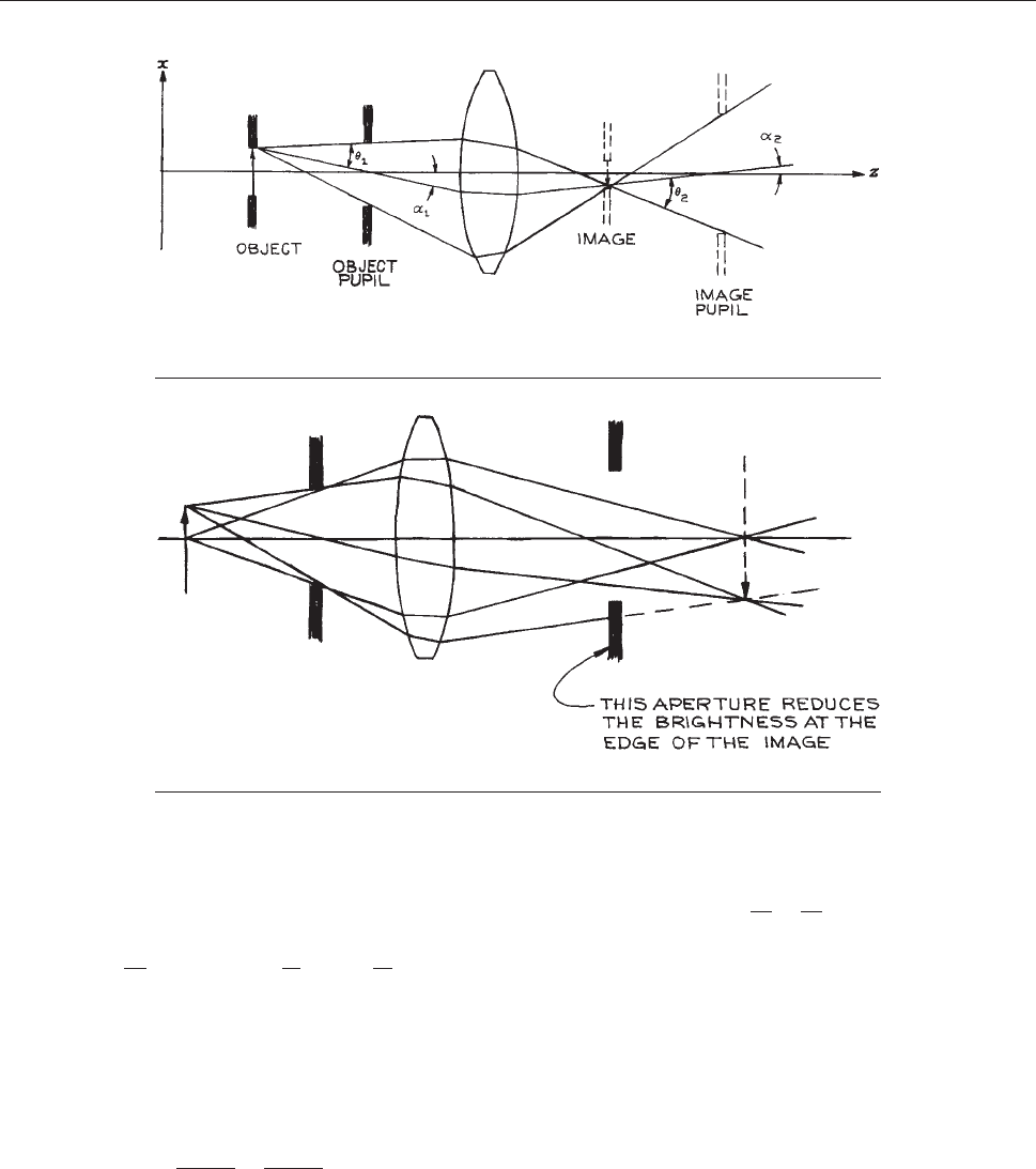
The image pencil angle is determined by the object pencil
angle. This relation is given to first order by the Helmholtz–
Lagrange law:
x
1
h
1
ffiffiffiffiffi
E
1
p
¼ x
2
h
2
ffiffiffiffiffi
E
2
p
ffiffiffiffiffi
E
1
E
2
r
¼ Mm; M ¼
x
2
x
1
, m ¼
h
2
h
1
ð5:4Þ
where M and m are the linear and angular magnifications,
respectively.
The current I
1
through the object window, that falls within
the object pupil is the same as the current I
2
through the
image window and pupil. Setting I
1
¼ I
2
¼ I, it follows that:
I
E
1
h
2
1
x
2
1
¼
I
E
2
h
2
2
x
2
2
ð5:5Þ
Furthermore, if b
1
and b
2
are the brightnesses of the object
and image, respectively, then this equality can be written:
b
1
E
1
¼
b
2
E
2
ð5:6Þ
demonstrating that the ratio of brightness to energy is
conserved from object to image.
5.1.4 Vignetting
The foregoing discussion assumes that the object radiates
uniformly; to the extent that the pencil angles are the same
for all points on the object, it follows that the image is
uniformly illuminated. However, if, as illustrated in Figure
5.4, a second pupil is added to the system, the illumination
Figure 5.3 Relation of image pencil angle h
2
and beam angle a
2
to object pencil angle h
1
and beam angle a
1
.
Figure 5.4 Vignetting.
326 CHARGED-PARTICLE OPTICS
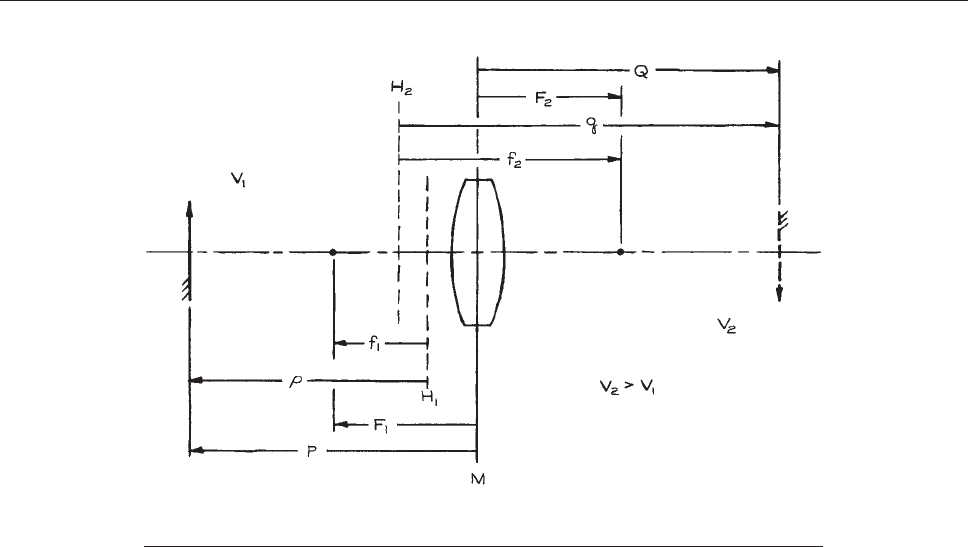
will vary across the image. Such a situation is called
vignetting. The one case in which an aperture, in addition
to the object window and pupil, does not produce vignet-
ting is when an aperture is placed at the location of the
image of the original window or pupil. Such an aperture is
sometimes employed to skim off stray current resulting
from scattering from slit edges and from aberrations. Also,
an aperture is placed at the exit window of an energy or
momentum analyzer to define its resolution. Except for
‘‘spatter apertures’’ or resolving apertures, an electron-
optical system should have only two apertures.
5.2 ELECTROSTATIC LENSES
It is a simple matter to produce axially symmetric electro-
des that, when electrically biased, will produce equipoten-
tial surfaces with shapes similar to those of optical lenses.
A charged particle passing across these surfaces will be
accelerated or decelerated, and its path will be curved so as
to produce a focusing effect. The chief difference between
such a charged-particle lens and an optical lens is that the
quantity analogous to the refractive index, namely the par-
ticle velocity, varies continuously across an electrostatic
lens, whereas a discontinuous change of refractive index
occurs at the surfaces of an optical lens. Charged-particle
lenses are ‘‘thick’’ lenses, meaning that their axial dimen-
sions are comparable to their focal lengths.
5.2.1 Geometrical Optics of Thick Lenses
In the case of a thick lens, it is not correct to measure focal
distances from a plane perpendicular to the axis through
the center of the lens. The focal points of a thick lens are
located by focal lengths, f
1
and f
2
, measured from principal
planes, H
1
and H
2
, respectively. As shown in Figure 5.5,
the principal planes of a charged-particle lens are always
crossed, and they are both located on the low-voltage side
of the midplane, M, of the physical lens. F
1
and F
2
locate
the focal points with respect to the central plane and hence
the distances from the central plane to the principal planes
are F
1
f
1
and F
2
f
2
, respectively. The object and image
distances with respect to the principal planes are p and q,
and, with respect to the central plane, are P and Q, respec-
tively. All distances are positive in the direction indicated
by the arrows in Figure 5.5.
Figure 5.5 Lens parameters. H
1
and H
2
are the principal planes. M is the midplane of the
physical lens.
ELECTROSTATIC LENSES 327
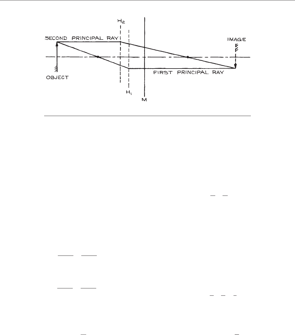
As in light optics, it is possible to graphically construct
the image produced by a lens if the cardinal points of the
lens are known. This procedure is illustrated in Figure 5.6.
It
is only necessary to trace two principal rays. From a
point on the object draw a ray through the first focal point
and thence to the first principal plane. From the point of
intersection with this plane draw a ray parallel to the axis.
Draw a second ray through the object point and parallel to
the axis. From the point of intersection of this ray with the
second principal plane, draw a ray through the second
focal point. The intersection of the first and second princi-
pal rays gives the location of the image point correspond-
ing to the object point.
A number of important relationships can be derived
geometrically from Figure 5.6 . The linear and angular
magnifi
cations, M and m, respectively, are given by:
M ¼
f
2
q
f
2
¼
f
1
f
1
p
ð5:7Þ
and
m ¼
f
1
p
f
2
¼
f
1
f
2
q
ð5:8Þ
where negative magnification implies an inverted image.
The object and image distances from the central
plane are
P ¼ F
1
f
1
M
ð5:9Þ
and
Q ¼ F
2
Mf
2
ð5:10Þ
The object and image distances from the principal planes
are related by Newton’s law:
p f
1
ðÞq f
2
ðÞ¼P F
1
ðÞQ F
2
ðÞ¼f
1
f
2
ð5:11Þ
and Newton’s formula:
f
1
p
þ
f
2
q
¼ 1 ð5:12Þ
For lenses that are not very strong, the principal planes are
close to the central plane. Then:
p ! P
q ! Q
ð5:13Þ
and
f
1
f
2
f
to give an approximate form of Newton’s formula that is
quite useful in the initial stages of design work:
1
P
þ
1
Q
¼
1
f
: ð5:14Þ
Furthermore, Spangenberg
1
has observed that for the
lenses discussed in succeeding sections:
M 0:8
Q
P
ð5:15Þ
Figure 5.6 Graphical construction of an image.
328 CHARGED-PARTICLE OPTICS
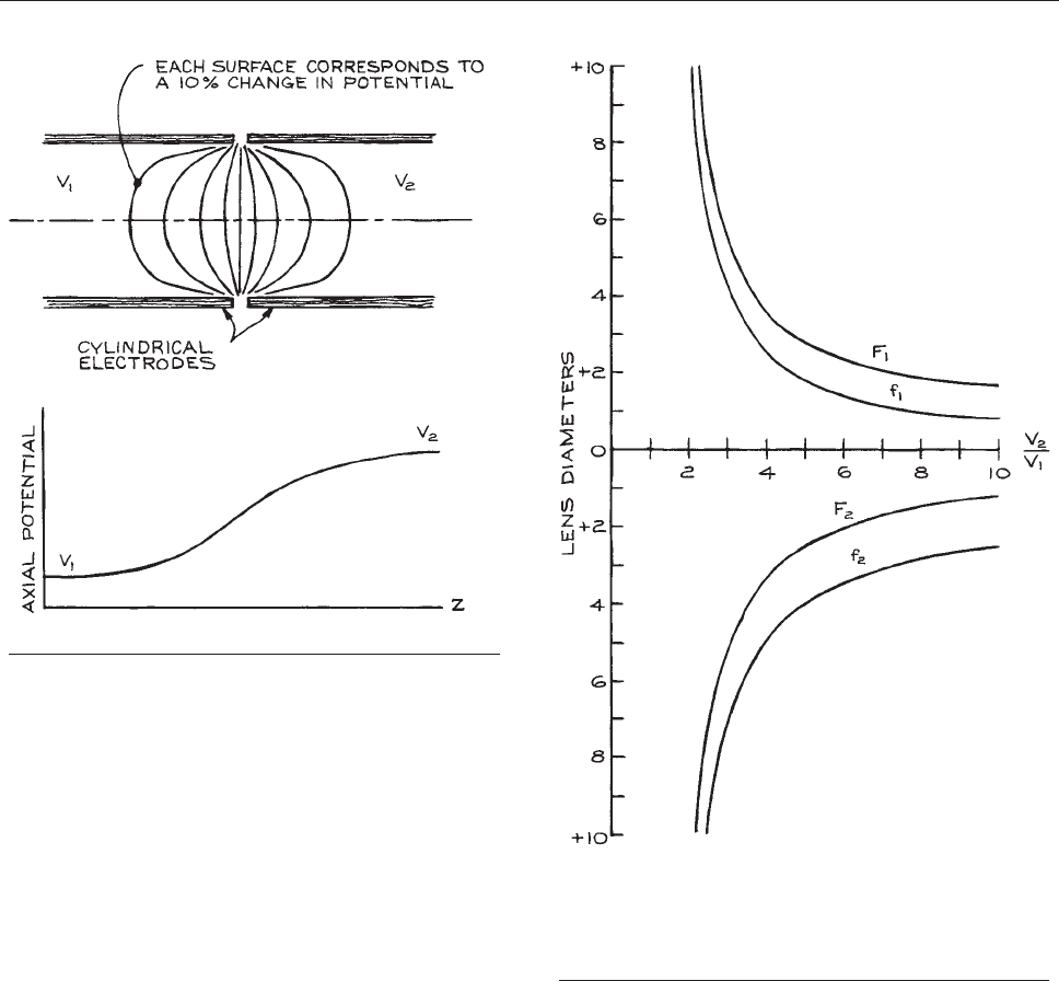
5.2.2 Cylinder Lenses
The most widely used lens for focusing charged particles
with energies of a few eV to several keV is that produced
by two cylindrical coaxial electrodes biased at voltages
corresponding to the desired initial and final particle ener-
gies. Figure 5.7 illustrates the equipotential surfaces and
the
axial electrical potential associated with the field pro-
duced by two coaxial cylinders biased at voltage V
1
and V
2
,
respectively.
The focal properties of a two-cylinder lens depend upon
the diameters of the cylinders, the spacing between them,
and the ratio E
2
/E
1
of the final to initial kinetic energies of
the transmitted particles. The lens properties scale with the
diameter, so all dimensions are taken in units of the diam-
eter D of the larger cylinder. If the gap between cylinders is
large, the focal properties become sensitive to the cylinder
wall thickness and external fields are liable to penetrate to
the lens. Most lenses are constructed with a gap g ¼ 0.1D.
The particle energies depend upon the electrical potentials
(bias voltages) applied to the elements. It is assumed that
the bias voltage supplies are referenced to the particle
source, so that V
2
/V
1
¼ E
2
/E
1
.
Focal properties are usually presented as g raphs (Figure
5.8)ortablesofF
1
, f
1
, F
2
,andf
2
as a fun ction of V
2
/V
1
.
For simple lenses i t is also convenient to plot P versus Q
for different V
2
/V
1
ratios, as in Figure 5.9. The c hief
Figure 5.7 Potential distribution in a two-cylinder lens.
Figure 5.8 Focal properties of a two-cylinder lens with
coaxial cylinders of the same diameter D and a gap
between of 0.1D. (From E. Harting and F. H. Read,
Electrostatic Lenses, Elsevier, New York, 1976; by
permission of Elsevier Publishing Company.)
ELECTROSTATIC LENSES 329
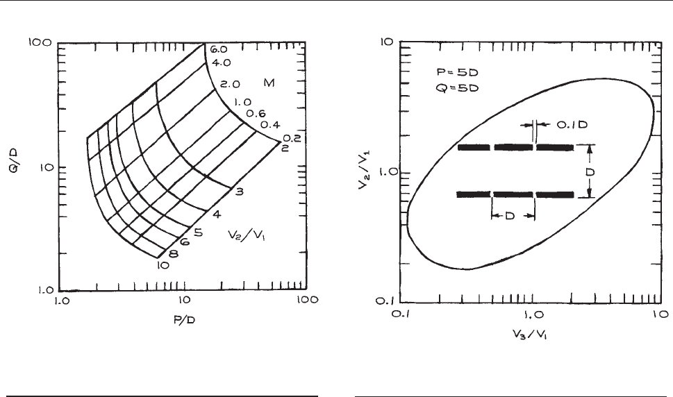
sources of information on the focal properties of electro-
static lenses are the book Electrostatic Lenses by Harting
and Read
7
and various journal articles by Read and his
coworkers.
8
These data are determined from numerical
solutions of the equation of motion of an electron in a lens
field and are thought to be accurate to 1–3%. Unfortunately,
these sources contain no information applicable to systems
with virtual objects or images. For two-cylinder lenses,
Natali, DiChio, Uva, and Kuyatt
9
have computed P–Q
curves that extend to negative values of the object and
image distances.
To obtain desired focal properties with a given accel-
eration ratio, two or more two-cylinder lenses can be
used in series. The lens field extends abou t one diameter
D on either side of the midplane g ap. When two gaps are
sufficiently close that their lens fields overlap, it is con-
venient to treat the combination as a single lens. Such a
three-cylinder lens has the advantage that it can produce
an image of a fixed object at a fixed image plane for a
range o f final-to-initial energy ratios. Alternatively, it can
produce a variable image location with a fixed energy
ratio.
A three-cylinder lens for which the initial and final ener-
gies differ is called an asymmetric lens. It can be used with
an electron or ion source to produce a variable-energy
beam. Such lenses are also used to focus an image of the
exit slit of a monochromator on a target while allowing for
a variation of the particle acceleration between monochro-
mator and target.
The focal properties of three-cylinder lenses are not
conveniently presented graphically, since each focal length
is a function of two independent variables. These variables
are usually taken to be V
2
/V
1
and V
3
/V
1
, where V
1
, V
2
, and
V
3
are the voltages on the first, second, and third lens
elements. Harting and Read
7
and Heddle
10
present data
on three-element lenses for V
3
/V
1
values between 1.0 and
30.0 in the form of tables of lens parameters (f
1
, f
2
, F
1
, F
2
)
as a function of V
2
/V
1
. They also plot ‘‘zoom-lens curves’’
as graphs of V
2
/V
1
versus V
3
/V
1
for selected values of P
and Q. An example is given in Figure 5.10.
Figure 5.9 P–Q curves for a two-cylinder lens with equal
diameter cylinders and a gap of 0.1D.(FromE.Hartingand
F. H. Read, Electrostatic Lenses, Elsevier, New York, 1976;
by permission of Elsevier Publishing Company.)
Figure 5.10 Typical ‘‘zoom-lens’’ curve. (From A. Adams
and F. H. Read, ‘‘Electrostatic Cylinder Lenses III,’’ J. Phys.,
E5, 156; copyright 1972 by the Institute of Physics.)
330 CHARGED-PARTICLE OPTICS
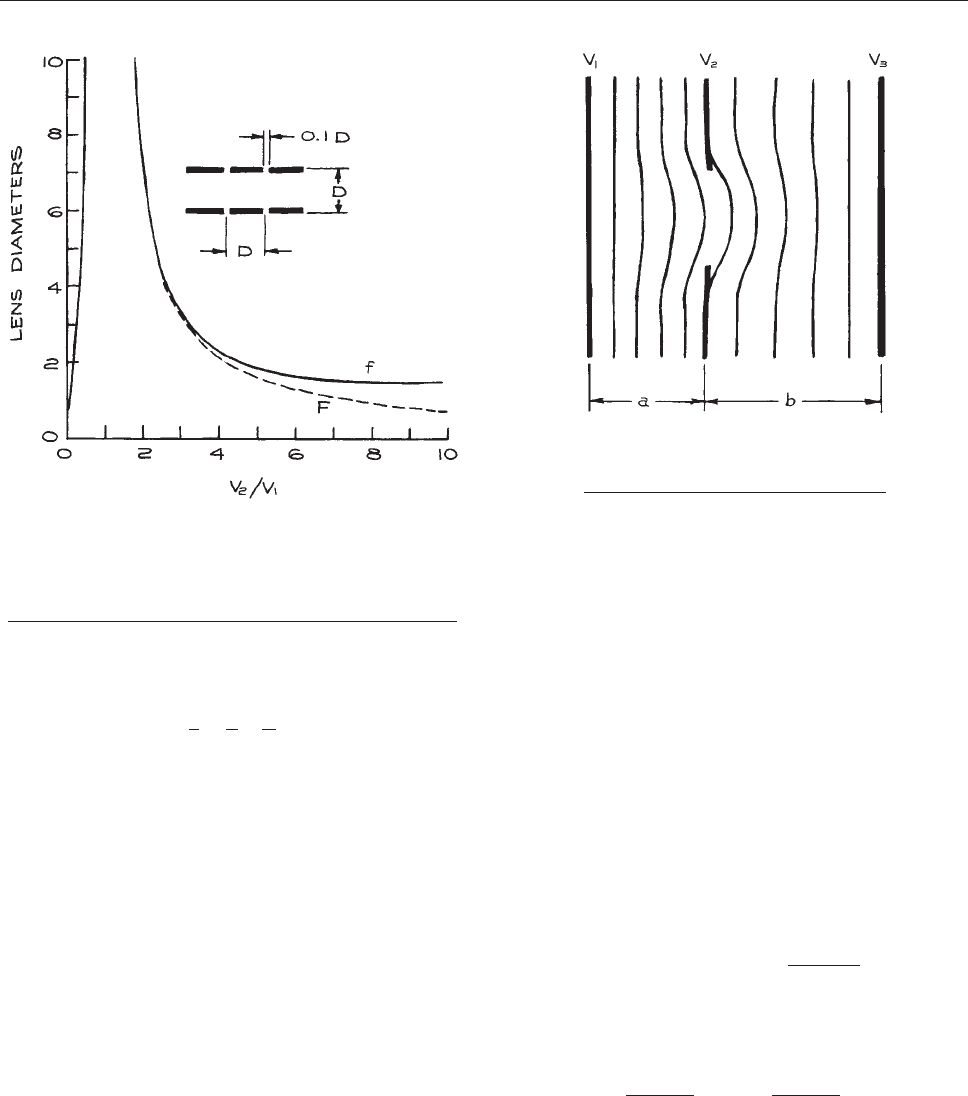
Read has defined a length f that approximately satisfies
the relation
1
f
¼
1
P
þ
1
Q
ð5:16Þ
for three-element lenses. For use in initial design work,
V
2
/V
1
is graphed as a function of f/D for various values
of V
3
/V
1
.
3
A three-element lens for which V
3
/V
1
¼ 1 is called an
einzel lens or unipotential lens. Such a lens produces focus-
ing without an overall change in the energy of the trans-
mitted particle. The focal properties are symmetrical: f
1
¼
f
2
¼ f and F
1
¼ F
2
¼ F. Figure 5.11 illustrates the focal
properties of a typical einzel lens. For any desired object
and image distance there are two focusing conditions: a
decelerating mode with V
2
/V
1
< 1 and an acceler ating
mode with V
2
/V
1
> 1. The ac celera ting mode is preferred,
because deceleration in the middle element causes expan-
sion of the transmitted beam, resulting in aberrations and
unwanted interactions with the lens surfaces.
5.2.3 Aperture Lenses
An aperture in a plane electrode separating two uniform-
field regions will have a focusing effect if the field on one
side is different from that on the other. As illustrated in
Figure 5.12, this lens results from a bulge in the equipo-
tential
surfaces caused by field penetration through the
aperture. A lens of this type is called a Calbick lens.
Single-aperture focusing is important in electron gun and
ion-source design because these devices usually have an
aperture at their output.
The Calbick lens is the analog of a thin lens. The electric
fields are established by the potentials V
1
, V
2
, and V
3
applied to the three planar elements, as shown in Figure
5.12. In this case it is assumed that electrons or ions
originate
at potential V
1
with essentially no kinetic energy.
For a circular aperture:
f
1
¼ f
2
¼ F
1
¼ F
2
¼
4V
2
E
B
E
A
ð5:17Þ
where the electrical field intensities in the uniform-field
regions are:
E
A
¼
V
2
V
1
a
, E
B
¼
V
3
V
2
b
ð5:18Þ
Figure 5.12 Protrusion of equipotential
surfaces through an aperture separating
regions of different field strength.
Figure 5.11 Focal properties of an einzel lens with the
intermediate cylinder of length A ¼ D and lens gaps
g ¼ 0.1D. (From E. Harting and F. H. Read, Electrostatic
Lenses, Elsevier, New York, 1976; by permission of
Elsevier Publishing Company.)
ELECTROSTATIC LENSES 331

The ratio of aperture potential to radius must be larger than
E
A
or E
B
. For a long slot in the xy plane:
F
x
¼
2V
2
E
B
E
A
ð5:19Þ
and
f
y
‘ ð5:20Þ
when the short dimension of the slot is in the x-direction.
The focal properties of a slot are important in the design
of electron guns that employ a ribbon filament.
11
Lenses can also be constructed using two or more aper-
tures. Read has computed the properties of two-aperture
and three-aperture lenses.
7
,
8
In practice, concentric cylindrical mounts support circular-
aperture electrodes of an aperture lens. The focusing
effects of these cylindrical elements can be ignored if the
cylinder diameter is at least three times greater than the
aperture diameter.
5.2.4 Matrix Methods
A useful description of the charged-particle trajectories
through a focusing system can be formulated using
the matrix methods introduced in Section 4.2.2.A
pa
rticle trajectory through a system that is cylindrically
symmetrical about the z-axis is determined by (r,dr/dz ¼
r#, z), where r is the radial distance of the trajectory
from the axis at z. A trajectory through a plane perpendic-
ular to the central axis at z is represented by a
vector:
r
r
0
ð5:21Þ
The effect of a displacement in a field-free region from z
1
to z
2
is given by:
r
2
r
2
0
¼ M z
1
! z
2
ðÞ
r
1
r
2
0
ð5:22Þ
where the ray transfer matrix is:
M z
1
! z
2
ðÞ¼
1 Dz
01
, Dz ¼ z
2
z
1
ð5:23Þ
A lens can be represented as if its effect were confined to
the region between the principal planes. The matrix oper-
ating between the principal planes is:
M H
1
! H
2
ðÞ¼
10
1
f
2
f
1
f
2
0
@
1
A
ð5:24Þ
Consider, for example, a ray originating at a point on an
object at z
1
andpassingthroughapointonanimageatz
2
.The
trajectory at z
2
can be determined from the trajectory at z
1
by:
r
2
r
2
0
¼ M H
2
! z
2
ðÞM H
1
! H
2
ðÞM z
1
! H
1
ðÞ
r
1
r
1
0
ð5:25Þ
In terms of the parameters defined in Figure 5.5, the
displacement
between the object and the first principal
plane is P F
1
+ f
1
; thus:
M z
1
! H
1
ðÞ¼
1 P F
1
þ f
1
01
ð5:26Þ
and similarly:
M H
2
! z
2
ðÞ¼
1 Q F
2
þ f
2
01
ð5:27Þ
Substitution yields:
r
2
r
2
0
0
@
1
A
¼
F
2
Q
f
2
f
1
f
2
Q F
2
ðÞP F
1
ðÞ
f
2
1
f
2
F
1
P
f
2
0
B
B
@
1
C
C
A
r
1
r
1
0
0
@
1
A
ð5:28Þ
This transformation matrix is generally applicable to the
problem of tracing a trajectory through the field of a lens.
For the two-cylinder lens, DiChio, et al. have derived sim-
ple analytical expressions for the elements of the matrix.
12
When r
1
and r
2
refer to points in the object and image
planes, respectively, the diagonal elements of the transfor-
mation matrix are the linear and angular magnification.
Furthermore, the focusing condition given by Newton’s
formula requires the numerator of the upper right element
332 CHARGED-PARTICLE OPTICS
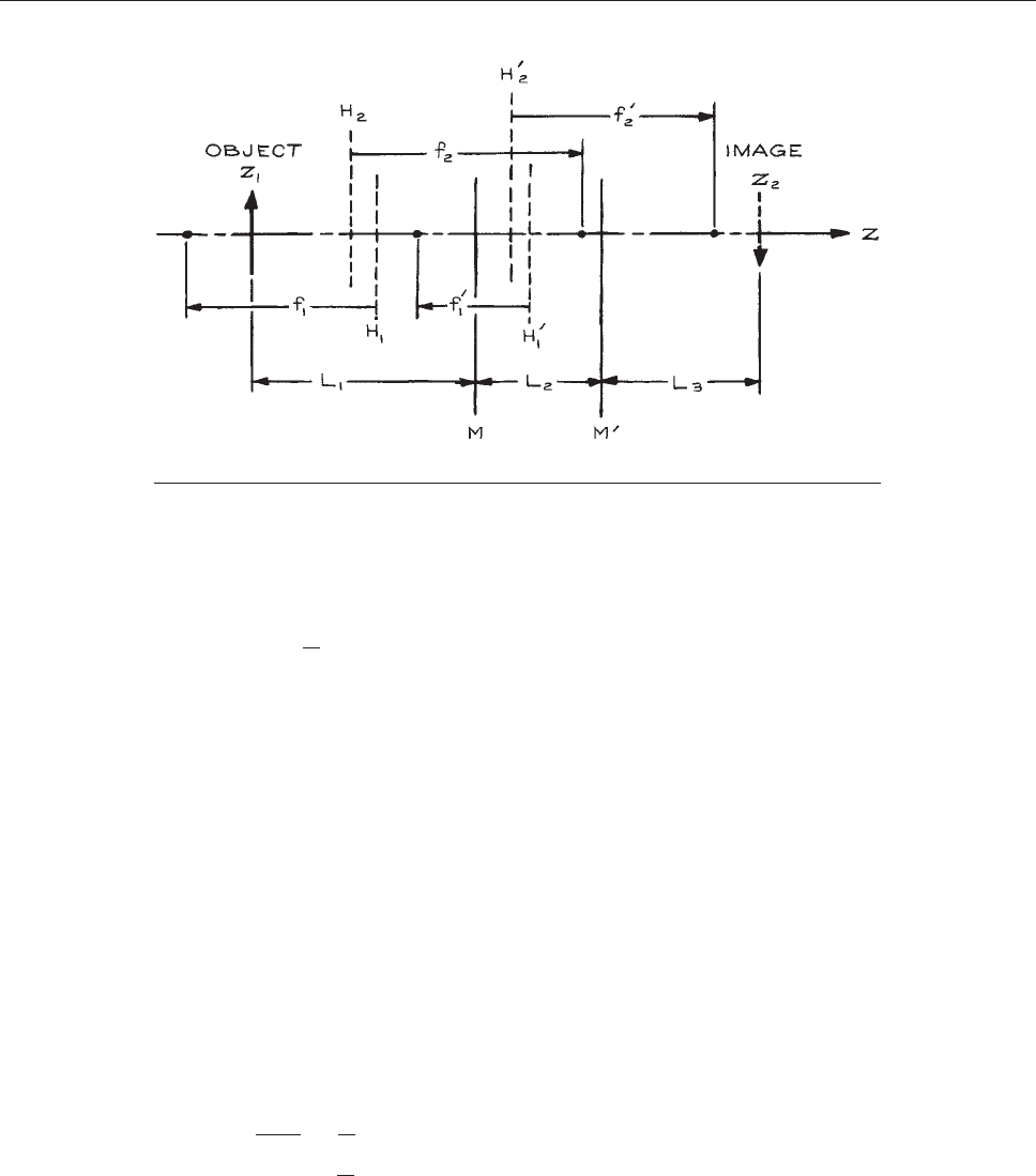
to be zero. Thus, the transformation matrix between object
and image is:
M object ! imageðÞ¼
M 0
1
f
2
m
!
ð5:29Þ
The matrix formulation is a desirable alternative to graph-
ical ray tracing for a system of lenses that are so close to
one another that an image does not appear between each
lens and the next. Consider, for example, the system of two
lenses in Figure 5.13. In this case the transformation
matrix
is:
M z
1
! z
2
ðÞ¼M H
2
0
! z
2
ðÞM H
1
0
! H
2
0
ðÞ
3 M H
2
! H
1
0
ðÞM H
1
! H
2
ðÞM z
1
! H
1
ðÞ
ð5:30Þ
In general, the image distance L
3
will be unknown initially.
It can be determined, however, from the focusing condition
that requires the upper right element of M z
1
! z
2
ðÞto be
zero.
It is occasionally necessary to determine a particle tra-
jectory in a region of uniform field. The transformation
matrix from z
1
to z
2
in a uniform field in the z-direction is:
M uniform fieldðÞ¼
1
2DzV
1
V
2
V
1
ffiffiffiffiffiffiffiffiffiffiffiffiffi
V
2
V
1
1
q
0
ffiffiffiffi
V
1
V
2
q
0
@
1
A
ð5:31Þ
where V
1
and V
2
are the potentials of the planar equipo-
tential surfaces perpendicular to the z-axis at z
1
and z
2
.
5.2.5 Aberrations
There are three types of aberrations that must be consid-
ered in designing charged-particle optics:
(1) Geometrical aberrations due to deviations from the
paraxial assumption that the angle h between a ray
and the central axis is sufficiently small that
h sin h tan h:
(2) Chromatic aberrations caused by variations in the
kinetic energies of transmitted particles.
(3) Space charge due to repulsive interactions between the
charged particles.
The geometrical aberration associated with a lens is
defined in terms of the radius Dr
2
of a spot in the image
plane formed by rays within the pencil angle h
1
that ema-
nate from an object point on the axis, as shown in Figure
5.14. The important geometrical errors can be expressed in
terms
of the coefficients of a power series in h
1
:
Dr
2
¼ bh
2
1
þ ch
3
1
... ð5:32Þ
Figure 5.13 A compound lens system.
ELECTROSTATIC LENSES 333
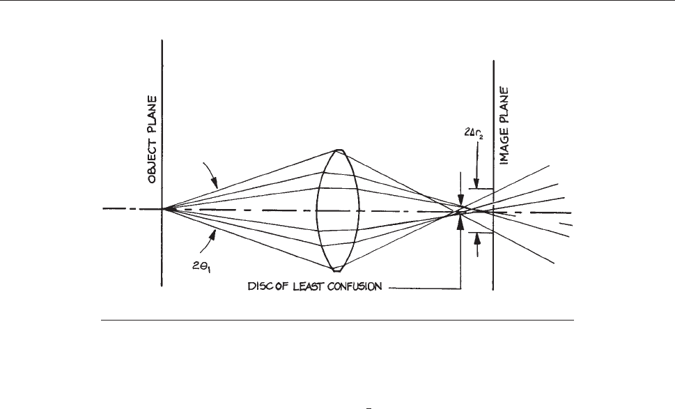
An imaging system is said to be second-order-focusing
if b ¼ 0, and third-order-focusing if c ¼ 0. An axially
symmetric system is always at least second-order-focusing,
since only terms of odd order appear in the expansion of
Dr
2
. The coefficient c is referred to as the third-order-
aberration coefficient. Higher-order coefficients can usu-
ally be ignored. For an object point on a lens axis, the error
represented by c is spherical aberration. Harting and
Read
7
have computed spherical-aberration coefficients
C
s
defined by:
c ¼ MC
s
ð5:33Þ
for all of the lenses for which they give focal properties.
For object points off axis, other types of aberration must
be considered (coma, field curvature, distortion, and
astigmatism). Most off-axis aberrations can be relate d
to the magnitude of C
s
. When the object is small com-
pared to the lens diameter, the spherical-aberration coef-
ficient gives a reasonable measure of the total geome trical
aberration.
As can be seen from Figure 5.14, the pencil of ray s
e
manating from a n object point achieves a minimum
diameter at a point slightly in front of the image plane.
This minimum diameter is the circle of least c onfu sion .
To achieve the shar pe st focus it is often possib le to vary
the lens voltages so as to place the circle of least confu-
sion on the desi red image pla ne. The radi us of this circle
is
1
4
Dr
2
;thusC
s
can, i n practice, be redu ced by a factor
of four.
The diameter of the bundle of rays emanating from an
object is usually determined by a pupil that limits the
portion of the lens that is illuminated by rays from the
object. The extent of illumination is specified by a filling
factor, which is the ratio of the diameter of the bundle of
rays near the lens gap to the lens diameter. Because the
spherical aberration depends upon the third power of the
angle between the limiting ray and the axis, it is obvious
that aberration increases rapidly with increasing filling
factor. In practice, a lens system should not be designed
with a filling factor in excess of about 50%.
For an object of finite extent, the worst aberration occurs
for off-axis image points. The magnitude of the aberration
depends upon the maximum value of the angle of a ray
from the edge of the object relative to the central axis of
the lens system. From Figure 5.3 it can be seen that this
angle
is the sum of the object pencil angle and beam angle.
In many lens systems, the image produced by one lens
serves as an object for succeeding lenses. According to
the Helmholtz–Lagrange law, the pencil angle associated
with this intermediate image is determined by the pencil
Figure 5.14 Geometrical aberration of the image of a point.
334 CHARGED-PARTICLE OPTICS
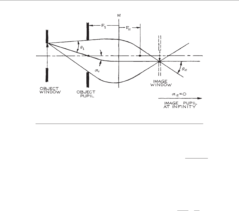
angle associated with the initial object. There are, how-
ever, no such physical restrictions on the beam angle from
the intermediate image. In fact, as shown in Figure 5.15,if
an
object pupil is placed at the first focal point of a lens,
then the corresponding image pupil is at infinity and the
image beam angle is zero. Obviously such an arrangement
reduces aberrations produced by lenses that treat this
image as an object.
Chromatic aberration depends upon the relative spread
in particle energies, DE/E, passing through a lens. Varia-
tions in particle energies can occur because of conditions
in the particle source or within the lens. An energy spread
of 0.2 to 0.4 eV is characteristic of electron sources. Some
ion sources yield ions in an energy bandwidth as great as
30 eV. Energy variations may also be caused by fluctua-
tions in the voltage from the power supplies that establish
both source and lens-element potentials.
For a given lens, the extent of chromatic aberration can
best be determined from a calculation of the image dis-
tances for particles with energies at the extremes of the
anticipated energy distribution. Consider, for example,
the case of a source at ground potential that produces
particles with energies between 0 and DE. For a lens of
voltage r atio V
2
/V
1
,adistanceP from the source, deter-
mine the corresponding image position, Q ¼ f(P, V
2
/V
1
).
Determine also:
Q þ DQ ¼ fP,
V
2
DE = q
V
1
DE = q
ð5:34Þ
Then a point on axis at the source yields an image at Q
of radius:
Dr
2
¼ h
2
DQ ð5:35Þ
or, by the Helmholtz–Lagrange law:
Dr
2
¼
h
1
DQ
M
ffiffiffiffiffiffi
V
2
V
1
r
ð5:36Þ
where h
1
and h
2
are the pencil angles at the source and the
image, respectively.
In electron-beam devices, the main cause of chromatic
aberration is the spread of electron kinetic energies emitted
from a thermionic cathode as well as the potential drop
across the emitting portion of the cathode. The energy of
electrons at the maximum of the current distribution from a
cathode is:
E
max
¼ 8:6 3 10
5
T eV ð5:37Þ
Figure 5.15 An object pupil at the first focal point moves the image
pupil to infinity and reduces the image beam angle a
2
to zero.
ELECTROSTATIC LENSES 335
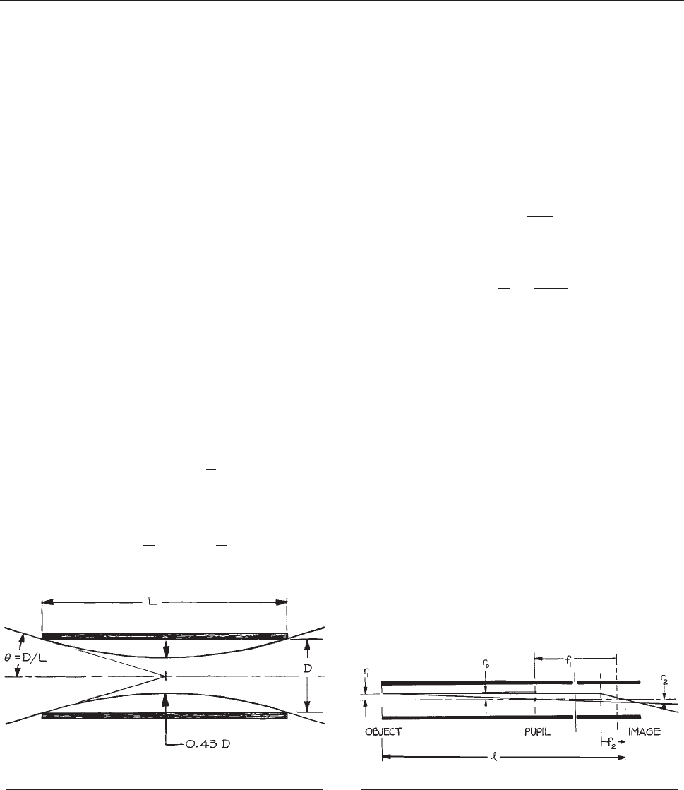
The width of the distribution DE E
max
.
For a bare tungsten filament, a temperature of
about 3000 K is required to produce significant emission.
At this temperature DE 0:25 eV. An oxide-coated cath-
ode (available from Electron Technology) can be
operated at temperatures as low as 1200 K, where
DE 0:1 eV. The potential drop across the emitting por-
tion of the cathode may add several tenths of an eV to the
energy spread.
The space-charge effect arises from the mutual r epul-
sion of particles of like charge. The effect increases with
current density. As a result, even a focused beam will
give a diffuse image. Furthermore, the beam will diverge
away from the image more rapidly than predict ed by
geometrical optics.
Space charge places a limit on the current in a charged-
particle beam. As an example of practical value, consider
the problem of transmitting maximum current through
a cylindrical element of length L and diameter D.As
shown in Figure 5.16, the maximum current is achieved
by
focusing the beam on a point at the center of the
tube with a pencil angle h ¼ D/L. It can be shown that
the space-charged-limited current of electrons of energy
E ¼qV is
I
max
ðelectronsÞ¼38:5V
3=2
D
L
2
lA ð5:38Þ
and the maximum ion current is:
I
max
ðionsÞ¼0:90
M
n
1=2
V
3=2
D
L
2
lA ð5:39Þ
where V is in volts, M is in amu, and n is the charge state.
2
The
minimum beam diameter at the space-charge limit is 0.43D.
Space charge also limits the current available from a
surface that emits electrons or ions. The typical source
geometry is the plane diode consisting of a planar anode
at potential V, a distance d from the cathode. Charged
particles produced by thermionic emission from the cath-
ode are accelerated toward the anode. The maximum elec-
tron current density at the anode is:
J
max
ðelectronsÞ¼2:34
V
3=2
d
2
lAcm
2
ð5:40Þ
while for an ion-emitting cathode:
J
max
ðionsÞ¼0:054
n
M
1=2
V
jj
3=2
d
2
lAcm
2
ð5:41Þ
with V in volts, d in cm, M in amu, and n the charge state.
5.2.6 Lens Design Example
Consider the problem of producing the image of the anode
aperture of an electron source on the entrance plane of an
energy analyzer, as illustrated in Figure 5.17. The anode
potential
is V
1
¼ 100 V, and the analyzer entrance-plane
potential is V
2
¼ 10 V. The anode aperture radius is
r
1
¼ 1.0 mm, and the distance from anode to analyzer is
l ¼10 cm. It is desired that the image of the anode aperture
serve as the entrance aperture for the analyzer with radius
r
2
¼ 0.5 mm. So as not to overfill the analyzer, one must
also have the image pencil angle h
2
¼ 0.14 and the image
beam angle a
2
¼ 0.
The lens to be designed is a decelerating lens with
V
2
/V
1
¼ 0.1 and magnification M ¼ 0.5. Customarily only
the focal properties of accelerating lenses are tabulated.
Figure 5.17 A simple lens design.
Figure 5.16 A beam focused to give maximum current
through a tube.
336 CHARGED-PARTICLE OPTICS

The focal properties for the desired lens are just the reverse
of those of the accelerating lens, with V
2
/V
1
¼ 10. From
Harting and Read,
7
the focal properties of the V
2
/V
1
¼ 10
lens (identified by a prime) are:
f
1
0
¼ 0:80DF
1
0
¼ 1:62D
f
2
0
¼ 2:54DF
2
0
¼ 1:19D
ð5:42Þ
The corresponding parameters for the V
2
/V
1
¼ 0.1 lens
are:
f
1
¼ 2:54DF
1
¼ 1:19D
f
2
¼ 0:80DF
2
¼ 1:62D
ð5:43Þ
From the P–Q curve of Figure 5.9 for V
2
/V
1
¼ 10 and
M#¼ 1/M ¼ 2, we estimate:
P ¼ Q
0
¼ 6:20D
Q ¼ P
0
¼ 2:05D
ð5:44Þ
Taking P ¼ 6.20D, Newton’s law gives:
Q ¼
f
1
f
2
P F
1
þ F
2
¼ 2:03D ð5: 45Þ
The overall length of the lens is:
l ¼ P þ Q ¼ 6:20D þ 2:03D ¼ 10 cm ð 5 :46Þ
and thus:
D ¼ 1:22 cm: ð5:47Þ
In order for the image beam angle to be zero, the
object pupil should be placed at the first focal point of
the lens so that the image pupil is at infinity. The object
pupil must define a pencil angle h
1
that is consistent with
the required image pencil angle. By the Helmholtz–
Lagrange law:
h
1
¼ Mh
2
ffiffiffiffiffiffi
V
2
V
1
r
¼ 0:022 ð5:48Þ
This angle is determined by the radius r
p
of an aperture at
the first focal point:
r
p
¼ h
1
P F
1
ðÞ¼0:13 cm ð5:49Þ
To estimate the geometrical aberration of this lens, we
calculate the spherical aberration for the lens used in
reverse. This is necessary because spherical-aberration
coefficients are available only for lenses with V
2
/V
1
>1.
For V
2
/V
1
¼ 10, Harting and Read give:
M
0
C
s
D
¼ 20 ð5:50Þ
Thus for the lens used in reverse, the image of a point is a
spot of diameter
Dr
0
¼ M
0
C
s
h
3
2
¼ 0:067 cm ð5:51Þ
For the lens used as designed, the size of the image of an
object point is:
Dr ¼ MDr
0
¼ 0:033 cm ð5:52Þ
Thus spherical aberration will enlarge the image by 67%
(Dr=r
2
¼ 0:033=0 :05); however, if the lens voltage is
adjusted slightly to bring the circle of least confusion onto
the image plane, the spherical aberration can be reduced
to 17%.
For a typical electron source, DE ¼ 0.3 eV. This energy
spread will result in chromatic aberration at the image. To
estimate this effect, calculate the image position Q + DQ
for electrons at the extreme of the energy distribution
where the deceleration ratio of the lens is:
ðV
2
DE=qÞ=ðV
1
DE=qÞ¼10:3=100:3 ¼ 0:103 ð5:53Þ
As before, the focal properties can be determined from
those of the corresponding accelerating lens. For the lens
with V
2
/V
1
¼ 0.103,
f
1
¼ 2:58DF
1
¼ 1:22D
f
2
¼ 0:82DF
2
¼ 1:65D
ð5:54Þ
The image position by Newton’s law in this case is:
Q þ DQ ¼
f
1
f
2
P F
1
þ F
2
¼ 2:07D ð5:55Þ
so:
DQ ¼ 0:04D ¼ 0:05 cm ð5:56Þ
This displacement of the image plane will cause the
image of a point object to appear as a disk of radius:
Dr ¼ DQh
2
¼ 0:007 cm ð5:57Þ
in the original image plane. Chromatic aberration enlarges
the image by about 14% (Dr=r
2
¼ 0:007=0:05).
ELECTROSTATIC LENSES 337

The overall aberration of the lens as designed is about
30%. The filling factor is:
2 h
1
þ a
1
ðÞP
D
¼ 54% ð5:58Þ
From the aberration calculations it can be seen that the
aberrations would become serious if the filling factor were
to exceed this value.
5.2.7 Computer Simulations
The re are a variety of progra ms available f or the compu-
tation of charged-particle t rajectories in the field of an
array of electrodes. Thes e employ Green’s func tion,
finite-element, and surface- charge methods to compute
the electrical field produced by the array. All provide
for the possibility of an applied magnetic field and some
solveforthefieldproducedbyanarrayofmagnets.A
particular virtue in computer-simulation programs is that
theycanbeusedtopredictthepropertiesofcompound
lenses that are more complex than the two- and three-
element lenses that are described above, and for which
there are tabulated values of focal lengths and focusing
properties. Among the most useful and widely used
simulation programs are Simion (Scientific Instrument
Services, Inc., www.simion.com) and CPO (CPO, Ltd.,
www.electronoptics.com).
It must be emphasized that computer simulation pro-
grams cannot substitute for an understanding of the basic
principles of electron optics described in this chapter. It is
impossible to obtain the desired performance in the design
of an electron-optical system by arbitrarily choosing an
array of electrodes and ‘‘fiddling’’ to obtain the desired
beam properties; the positions of lenses, windows, and,
especially, pupils should be determined from considera-
tions of basic principles before turning to the computer
to optimize a design or test its performance.
Figure 5.18(a) shows a computer simulation of the
simple
cylindrical lens discussed in Section 5.2.6 and
illustrated
in Figure 5.17. The computed electric field at
the
lens gap is shown as equipotential surfaces. Electron
trajectories are traced from points at the center and the
upper edge of the object win dow. One of the three tra jec-
tories from each point passes through the center of the
pupil; the other two are the extreme rays t hat can pass
through the pupil. Figure 5.18(b), a bl owup of a portion of
5.
18(a), shows the location of the image formed. It is
worth noting that the size of the image is half t hat of
the object, as predict ed in Section 5.2.6. The image dis-
tance, Q =1
.93D , is s om ewhat short of t ha t pred ic ted.
The bundle of rays from both the ce nter and the edge of
the object emerge from the image with their central axes
parallel to the axis of the lens; this implies that the beam
angle a
2
=0(seeFigure 5.15). Figure 5.18(c) shows a lens
system identical to that in 5.18(a), except the pupil has
been moved closer to the object and away from the first
focal point of the lens. The result is a significant increase
in the image beam angle, as well as noticeable geometric
aberration.
5.3 CHARGED-PARTICLE SOURCES
An electron or ion gun consists of a source of charged
particles, such as a hot metal filament or a plasma, and an
electrode structure that gathers particles from the source and
accelerates them in a particular direction to form a beam.
There is a wide range of practical electron and ion guns.
Some simple devices and their principles of operation will
be described in this section. In addition to simple devices
that can be conveniently constructed for laboratory use,
there are a number of very sophisticated guns that have been
developed commercially. These include electron guns for
cathode-ray tubes and electron-beam welders, and ion guns
for sputter-cleaning apparatus and for ion-implantation dop-
ing of semiconductors. Manufacturers of electron guns and
ion sources suitable for use in the laboratory include Kimble
Physics (electron and ion guns), Spectra-Mat (alkali-metal
ion sources), and Southwest Vacuum Devices and Clif-
tronics (both manufacturing CRT guns useful as electron
sources and both owned by Video Display Corporation).
5.3.1 Electron Guns
Electrons are produced by thermionic emission, field
emission, photoe lectric emission, a nd electron-impact
ionization. Thermionic sources are the most common.
13
These sources typically consist of a wire filament of
some refractory metal, such as tungsten or tantalum,
338 CHARGED-PARTICLE OPTICS
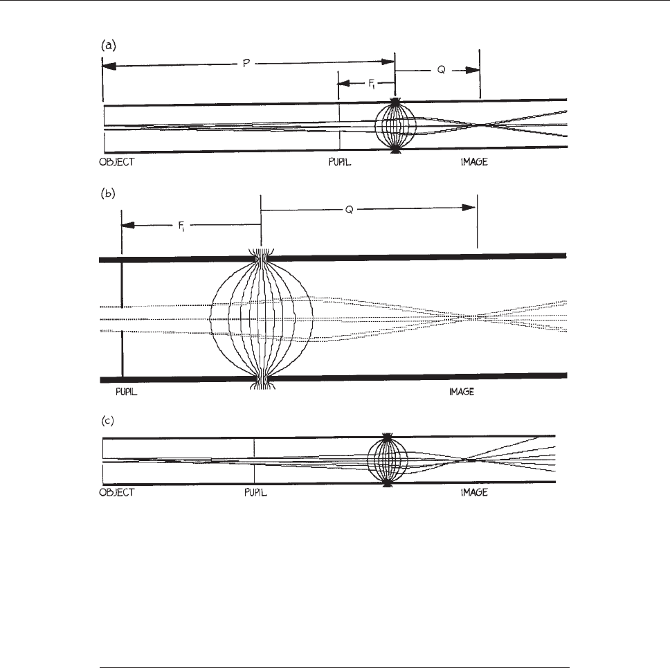
which is heated by an ele ctrical current passing through
it. In some cases thermionic sources consist of a metal
cup o r button that is indirectly heated by an electrical
heater or by e lectron bombardment of the back surfac e.
The electrons from a hot filament possess energies of a
few tenths of an electron volt. Mutual repulsion will
cause the electrons to diffuse away from the source if
they are not immediately accelerated into a beam. M any
accelerator structures are us ed. Most us e either diod e
(two-electrode) or triode (thre e-electrode) geometries ,
Figure 5.18 (a) MacSimion simulation of the cylindrical lens shown in Figure 5.17 and
discussed in Section 5.2.6. The voltage ratio V
2
/V
1
¼ 0.10; the object is defined by an aperture
window and the object distance from the lens gap is P ¼ 6.20D (D is the diameter); a pupil is
placed at the first focal point of the lens. The electric field at the lens gap is shown by
equipotential surfaces computed by the program. The trajectories of 100 eV electrons
originating at the center and edge of the window have been traced by the computer program.
(b) A blowup showing the image formed. The image distance from the lens gap is Q ¼ 1.93D.
(c) The same lens with the pupil moved closer to the object and away from the first focal point
of the lens. The result is a significant increase in the beam angle at the image.
(MacSimion, is a simulation program for MacIntosh developed by Don McGilvery and
coworkers, Department of Chemistry, Monash University, Clayton, Victoria, AUSTRALIA 3168)
CHARGED-PARTICLE SOURCES 339
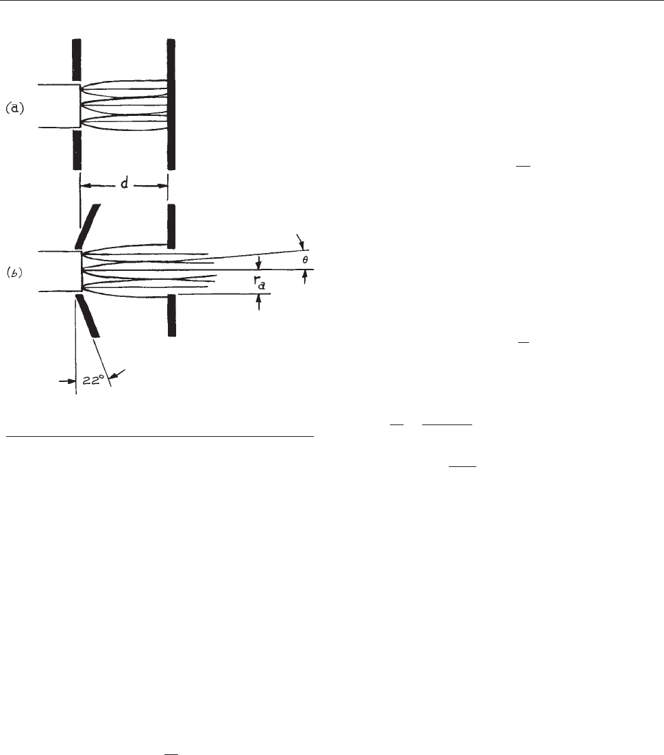
although some TV tubes employ a pentode geometry.
The Pierce diode geometry is most common in labora-
tory devices.
Figure 5.19(a) ill ustrates a simple diode electron gun
consisting
of a plane emissive surface and a parallel
plane anode. Electrons leave the cathode with a nomin al
energy E
k
. The anode is b iased at a positive potential V
a
relative to the ca thode, so that electrons from a spot on
the cathode will appear at a spot on the anode with ener-
gies of approximately E
a
= qV
a
. To admit the acceler-
ated electrons to the system beyond, a hole is made in the
anode. If the cathode and anode were infinite in extent, the
space-charge-limited current density given in Section 5.2.5
could be achieved at the anode, and the electron beam
emer
ging from the anode hole would be characterized by
a beam angle:
a ¼
r
a
3d
ð5:59Þ
where r
a
is the radius of the anode hole and d the cathode-
to-anode spacing. Since the most divergent electron
arriving at the anode would be one emitted parallel t o
the cathode with energy E
k
, it can be seen that the pencil
angle characterizing the beam from the anode aperture
would be
h ¼
ffiffiffiffiffi
E
k
E
a
r
ð5:60Þ
For a cathode of finite extent, the space-charge interac-
tion causes the beam to spread laterally within the gap
between cathode and anode. Pierce
2
has shown that the
electric field in an infinite space-charge-limited diode
can be reproduced in the region of a finite cathode by
means of the conical cathode structure illustrated in Figure
5.19(b). The maximum current of electrons is:
I
max
¼ pr
2
a
J
max
¼ 7:35
r
a
d
2
V
3=2
a
lA ð5:61Þ
The corresponding ratio of brightness to energy (which is
conserved) is:
b
E
a
¼
I
max
E
a
p
2
r
2
a
h
2
¼ 0:74
E
3=2
a
E
k
d
2
lAcm
2
sr
1
eV
1
ð5:62Þ
The design of multielectrode guns is a complicated
process involving time-consuming experimentation. A
number of special guns have been developed for such pur-
poses as producing low-energy electron beams or very
narrow beams. Klemperer and Barnett describe many of
these,
3
and most can be constructed easily if they are really
needed. In general, however, it is best to use the simplest
device that will fulfill one’s requirements.
The guns developed for TV tubes are the pro duct of
much industrial development. These guns will produce a
beam of electrons of several hundred eV to several tens
of thous ands eV th at is sharply focus ed to a spot at a
distance of 10 to 20 cm. Cathode-ray -tube guns can be
obtained quite inexpensively from commercial suppliers
such as Southwest Vac uum Devices and Cliftronics
(both owned by Video Display Corporation). Special-
ized guns of similar design are available from Kimble
Figure 5.19 (a) The plane diode; (b) the Pierce geometry
that simulates the field of the plane diode.
340 CHARGED-PARTICLE OPTICS
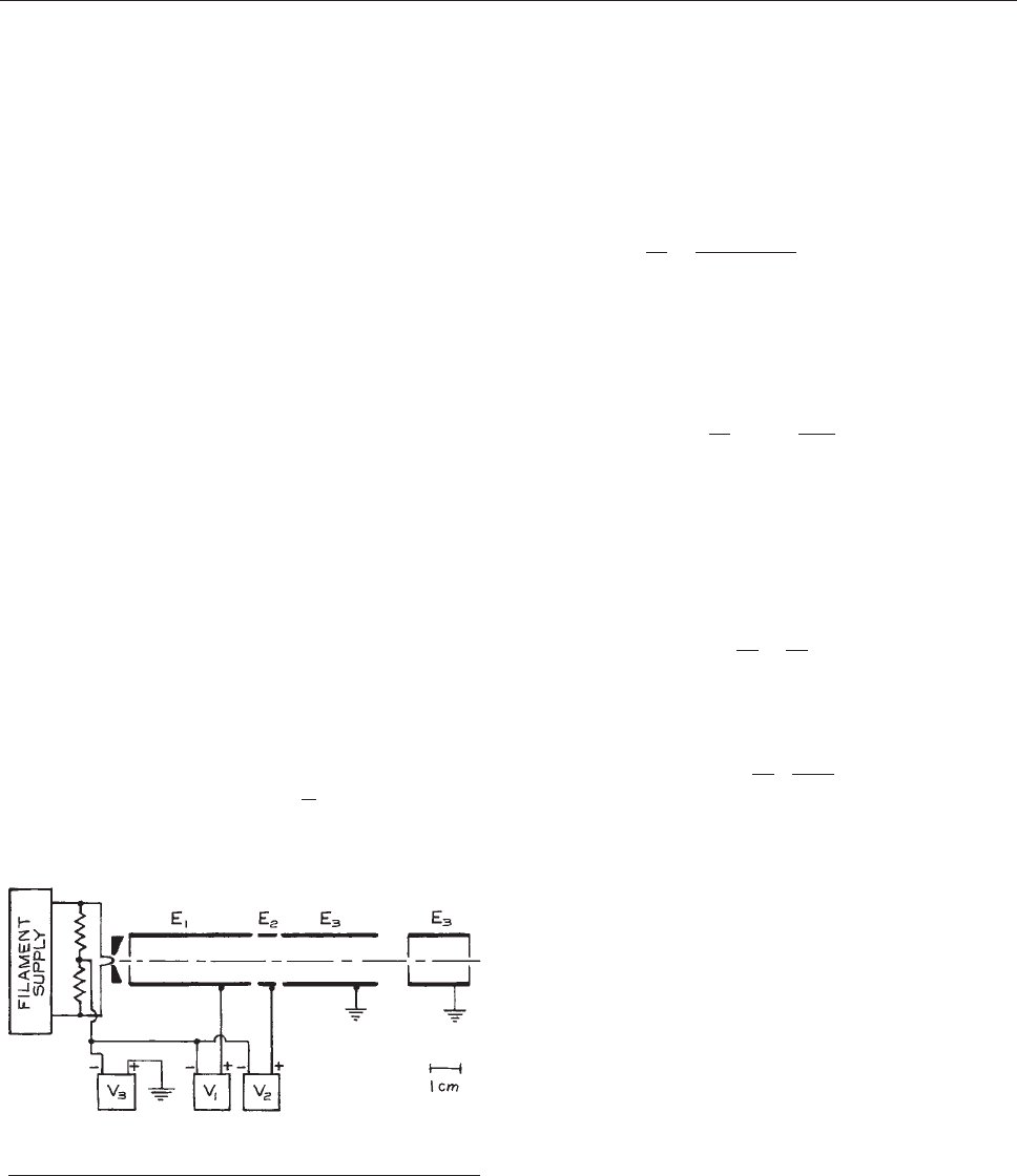
Physics and other manufacturers of electron spe ctro-
meters.
5.3.2 Electron-Gun Design Example
Consider the problem of designing an electron gun consist-
ing of a Pierce diode and a lens system that can inject a
beam of 20–200 eVelectrons into a gas cell, as illustrated in
Figure 5.20. It is desired that the beam current approach the
sp
ace-charge limit at 20 eV. The overall length of the gun is
to be about 10 cm, and the cell is to be located 4 cm in front
of the gun. The cell is 2 cm long, with an input aperture of
radius r
2
¼ 0.1 cm and an exit aperture of radius 0.15 cm.
Treat the exit aperture as though its radius r
4
were 0.1 cm, so
as to make the beam tight enough to minimize backscatter-
ing of electrons from the edges of this aperture.
Note that the electron gun system in Figure 5.20 is wired
in
such a way that the energies of the electrons through the
system, E
1
, E
2
, and E
3
, in electronvolts, are numerically
equal to the power supply voltages V
1
, V
2
, and V
3
. This is,
in general, a great convenience, since electron energies can
be read directly from the power supplies. In the following
discussion, E
i
and V
i
can be used interchangeably.
The maximum current through the cell can be taken as the
space-char ge-limite d current through a cylinder with a diam-
eter D equal to that of the gas-cell apertures and length L equal
to the length of the gas cell. From Section 5.2.5, the maximum
curr
ent of electrons with energy E
3
¼ 20 eV is, in this case
I
max
¼ 38:5V
3=2
3
D
L
2
¼ 34:4 lA
ð5:63Þ
To approach this limit, focus an image of the anode
aperture on the center of the cell. Make the image radius
r
3
¼ 0.43r
2
, the minimum size of the space-charge-limited
beam (note Section 5.2.5 and Figure 5.16).
14
The image
pencil angle will be h
3
¼ D/L ¼0.1 and the ratio of bright-
ness to energy at this image is:
b
3
E
3
¼
I
max
=p
2
r
2
3
h
2
3
E
3
¼ 9500 lAcm
2
sr
1
eV
1
ð5:64Þ
At the anode of the Pierce diode (Section 5.3.1), the ratio
of
brightness to energy is given by:
b
1
E
1
¼ 0:74
E
3=2
1
E
k
2
ð5:65Þ
where E
k
is the mean kinetic energy of electrons emitted
by the cathode, and E
1
is the energy of electrons at the
anode that is held at the potential V
1
relative to the cathode.
Now the ratio of brightness to energy is a conserved quan-
tity, so:
b
1
E
1
¼
b
3
E
3
ð5:66Þ
Substituting from the previous two equations yields:
E
1
¼
b
3
E
3
E
k
d
2
0:74
2=3
ð5:67Þ
For E
k
¼0.25 eV (Section 5.2.5), a cathode-to-anode spac-
ing d ¼ 0.5 cm, and a final electron energy of 20 eV, the
kinetic energy of electrons at the anode, E
1
¼ 86 eV, and
the potential to be applied to the anode is:
V
1
ðE
3
¼ 20 eVÞ¼86 V ð5:68Þ
A similar calculation yields:
V
1
ðE
3
¼ 200 eVÞ¼185 V ð5:69Þ
The current from the diode depends upon the radius of
the anode aperture r
1
and the current density J at the anode:
I ¼ Jpr
2
1
ð5:70Þ
Figure 5.20 An electron gun system to inject a
variable-energy beam into a gas cell.
CHARGED-PARTICLE SOURCES 341

With the lens system tuned to inject 20 eV electrons into
the target cell (E
3
¼ 20 eV), the maximum current density
at the anode: is
J
max
¼
2:34
d
2
V
3=2
1
; V
1
¼ V
1
ðE
3
¼ 20 eVÞ
¼ 7500 lAcm
2
ð5:71Þ
To achieve maximum current in the cell at 20 eV, we
choose the anode aperture to be:
r
1
¼
I
max
pJ
max
1=2
¼ 0:04 cm ð5:72Þ
A similar calculation for E
3
¼ 200 eV would suggest
using a larger anode aperture; a larger aperture, however,
would produce an excess of current and thus many stray
electrons when the system is tuned to produce a low-
energy beam.
Note that when the system is designed to approach
the space-charge limit at 20 eV, the pencil angle at the
anode is consistent with the pencil angle defined by the
cell apertures. The pencil angle characteristic of the Pierce
diode at the low-energy limit is:
h
1
¼
ffiffiffiffiffi
E
k
E
1
r
¼
ffiffiffiffiffiffiffiffiffi
0:25
86
r
¼ 0:05 ð5:73Þ
and the anode pencil angle that gives the space-charge-
limited pencil angle in the cell can be determined from
the Helmholtz–Lagrange law:
h
1
¼
ffiffiffiffiffi
E
k
E
1
r
r
3
r
1
h
3
¼ 0:05 ð5:74Þ
For final energies greater than 20 eV, these pencil angles
will be less than the angle defined by the cell apertures,
and scattering from the edges of the apertures will be
minimized.
It remains to design a lens system that will image the
anode aperture on the center of the gas cell. A variable-ratio
lens is required, and in this case a three-cylinder asymmetric
lens seems appropriate. The voltage ratios at the extremes
of the desired operating conditions are:
V
3
V
1
E
3
¼ 20 eVðÞ¼0:23 ð5:75Þ
and
V
3
V
1
E
3
¼ 200 eVðÞ¼1:1 ð5:76Þ
The desired magnification is
M ¼
r
3
r
1
1 ð5:77Þ
The lens diameter must be chosen to give an acceptable
filling factor. As a starting point, recall that:
M 0:8
Q
P
ð5:78Þ
The lens is to focus the anode aperture on the center of the
gas cell, so P + Q ¼ 10 cm + 4 cm + 1 cm ¼ 15 cm. The
distance from the anode to the middle of the lens will be:
P ¼
P
P þ Q
3 15 cm
¼
P
P þ 1:25MP
3 15 cm
¼ 6:7cm
ð5:79Þ
For a final energy of 20 eV, the maximum diameter of
the beam through the lens system will be approximately:
2h
1
P ¼ 0:67 cm; h
1
ðE
3
¼ 20 eVÞð5:80Þ
Choose D ¼ 2.0 cm to achieve a filling factor less than
30%. Then:
P ¼ 3:35D
Q ¼ 4:15D
ð5:81Þ
and the nominal focal length of the desired lens (see Sec-
tion
5.2.2)is
f ¼
1
P
þ
1
Q
1
¼ 1:85D ð5:82Þ
The calculations of Adams and Read
8
or Harting and
Read
7
can then be used to determine the lens voltages that
correspond to this nominal focal length. Alternatively, the
lens system can be modeled by computer simulation and
the potential to be applied to the central element of the
342 CHARGED-PARTICLE OPTICS
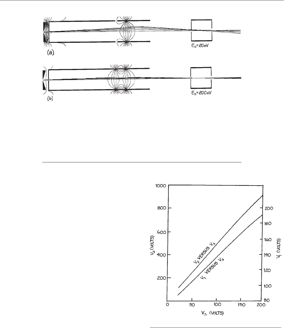
three-cylinder lens can be determined empirically. Figure
5.21 shows the results of simulations for the projection of
20
and 200 eV electrons into the target cell. Figure 5.22
gives the central lens element voltage V
2
obtained from the
simulation.
5.3.3 Ion Sources
Many parameters must be considered in choosing or
designing an ion source. Foremost is the desired type of
ionic species and charge state. The physical and chemical
properties of the corresponding parent material determine
to a large extent the means of ion production. Other impor-
tant parameters are the desired current, brightness, and
energy distribution. In some cases it is also necessary to
consider the efficiency of utilization of the parent material.
In view of the number of variables involved, it is not
surprising that many different types of ion sources have
been developed to meet both scientific and industrial
demands.
15
Ion sources can be classified according to the ion pro-
duction mechanism employed. The two most common
Figure 5.21 MacSimion simulat ion of the electric field and electron traject ories in the
electron gun system shown s chematically in Figure 5.20. The cathode-to-anode
distance
in the Pierce diode is d ¼ 0.5 cm and the radius of the aperture in the anode is
r
1
¼ 0.04 cm. The radii of the apertures in the target cell are r
3
¼ 0.1 cm and r
4
¼ 0.15
cm. The diameter of the lens D ¼ 2 cm, the length of the central element A ¼ 0.5D,and
the gap between lens elements is g ¼ 0.1D. (a) Trajectori es of electrons that pass
through the cell with energy E
3
¼ 20 eV; V
1
¼ 86 V, V
2
¼ 105 V, and V
3
¼ 20 V. (b)
Trajectories of electrons that pass through the cell with energy E
3
¼200 eV; V
1
¼185 V,
V
2
¼ 960 V, and V
3
¼ 200 V.
Figure 5.22 Lens voltages for the lens system of Figure 5.20.
CHARGED-PARTICLE SOURCES 343
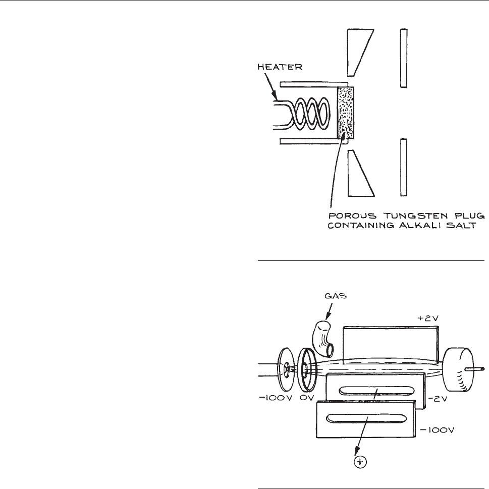
means are surface ionization and electron impact. The
electron-impact sources include both electron-bombard-
ment sources and plasma sources. More exotic ion sources
employ ion impact, charge exchange, field ionization, and
photoionization. Three typical sources, illustrating differ-
ent ion production mechanisms, will be discussed below.
In practice, the simplest means of producing ions is by
thermal excitation of neutral species. This process, known
as surface ionization, occurs efficiently when an atom or
molecule is brought in contact with a heated surface whose
work function exceeds the ionization potential of the atom
or molecule. This requirement is fulfilled for alkali atoms
(Li, Na, K, Rb, Cs) on surfaces of tungsten, iridium, or
platinum. In order for ionization to compete with vaporiza-
tion, it is necessary that the surface be sufficiently hot that
the substrate surface is only partially covered with neutrals,
so that the work function of the surface is characteristic of
the substrate rather than the material to be ionized.
In a surface-ionization ion gun, the source of neutral
atoms can either be remote from, or integral with, the ion-
izing surface. In the remote type, the alkali metal is con-
tained in an oven. A stream of metal vapor from the oven is
directed toward the ionizer, which is a heated metal ‘‘cath-
ode’’ located within an electrode structure similar to that
of an electron gun. The ‘‘anode’’ is negatively biased to
accelerate positive ions into a beam. The most convenient
alkali-ion emitter consists of a porous tungsten disk that
has been infused with an alkali-containing mineral and
mounted on an electrical heater. When heated, alkali atoms
are generated; the atoms diffuse to the surface of the disk,
and are ionized as they leave the surface. These emitters
with integral heaters are commercially available (Spectra-
Mat). As shown in Figure 5.23 , a source is constructed by
inserting
the emitter into the cathode of a Pierce diode or
into some other extractor electrode structure.
The majority of laboratory ion sources employ electron-
impact ionization. The simplest configuration is illustrated
in Figure 5.24 . In this source, an electron beam from a
simple
diode gun is injected into an ionization chamber
containing an appropriate parent gas. A transverse electric
field of a few V/cm causes ions produced by electron
impact to drift across the chamber and out through a slit
in the side of the chamber. An extractor electrode system
accelerates the ions into a beam. The ionic species pro-
duced will depend upon the parent gas, the gas pressure,
and the electron energy. Singly charged ions are produced
with maximum effi ci enc y at electron energies of about 70 eV.
Higher electron energies favor multiply charged ions.
Lower electron energies yield only singly charged ions and
Figure 5.23 An alkali-ion source consisting of an indirectly
heated emitter in a Pierce diode.
Figure 5.24 An electron-impact ion source.
344 CHARGED-PARTICLE OPTICS
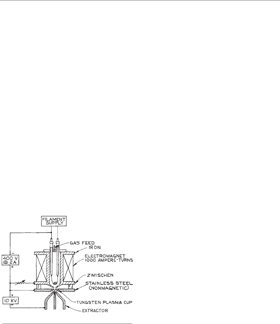
reduce the extent of fragmentation in the event that the
parent gas is a molecular species. Gas pressures are typi-
cally 1 to 10 mtorr. Higher pressures place an unreasonable
gas load on the vacuum system and impede the flow of ions
from the ionization chamber.
Theefficiencyoftheelectron-impact ionization source can
be improved by imposing a magnetic field of a few hundred
gauss coaxial with the electron beam. The field confines the
electron beam to a spiral around the beam axis, thus increas-
ing the path length and maximizing the probability of
collision with the gas molecules. Electron-bombardment
sources of this type yield currents of a fe w tens of micro-
amperes. The chief advantages are simplicity of construction
and an energy spread in the product ions of only a few eV.
Relatively high ion densities can be achieved in an elec-
trical discharge through a gas. The ion density in a dis-
charge can be further increased if the discharge is confined
and compressed by a magnetic field. The duoplasmatron
source illustrated in Figure 5.25 is the prototypical dis-
charge-
type ion source.
16
Applying a potential of 300 to
500 V between the heated cathode and the anode produces
a discharge through a gas at about 100 mtorr. After the arc
is struck, the discharge is maintained by passing a current
of 0.5 to 2 A through the ionized gas. In the duoplasma-
tron, the intermediate element, known as the zwischen, is
one pole of a magnet. The axial magnetic field at the tip
of the zwischen confines the discharge to a dense plasma
bubble at the anode. Plasma leaks through a hole in the
anode to fill a cup on the front face of the anode. An
extractor electrode, biased at about 10 kV relative to the
anode, withdraws ions from the surface of the plasma. Ion
currents of 1 to 10 mA are easily obtained. In operation,
several hundred watts of electrical power are dissipated in
the arc and the electromagnet. In its original form, this
source was liquid-cooled. However, the author has found
air-cooling to be acceptable for slightly smaller versions.
The duoplasmatron is the brightest of ion sources. Copious
quantities of singly charged atomic and diatomic ions can
be obtained for these species for which an appropriate
gaseous parent can be found. It is also possible to obtain
a few microamperes of doubly charged ions, and in addi-
tion, negative ions can be obtained by reversing the extrac-
tion potential.
17
The chief disadvantages of plasma sources
are their complicated construction and the fact that stable
operation is only possible for a few days before cleaning
and filament replacement are necessary.
5.4 ENERGY ANALYZERS
There are three basic means of measuring the energy of
charged particles in a beam. These involve measuring the
time of flight over a known distance, the retarding potential
required to stop the particles, or the extent of deflection in
an electric or magnetic field.
Because of the great velocities involved, the flight time
of a charged particle over any reasonable distance is very
short. Determination of the kinetic energy of a particle
from the time required to cover a distance of a few centi-
meters typically requires electronics with a response time
of a few nanoseconds. Time-of-flight analyzers are used for
energy analysis of electrons with energies less than 10 eV
and ions below 1 keV.
Placing a grid or aperture in front of a particle collector
and var ying the potential on this element will perform an
energy analysis of the particles in a beam.
18
This is a retard-
ing potential analyzer. The current at the collector is the
integrated current of particles whose energy exceeds the
potential established by the grid. As the grid potential is
reduced from that at which all current is cut off, the collector
current increases. To obtain the energy distribution, the inte-
grated current as a function of retarding potential must be
differentiated. One drawback to this method is that only the
Figure 5.25 A duoplasmatron ion source.
ENERGY ANALYZERS 345
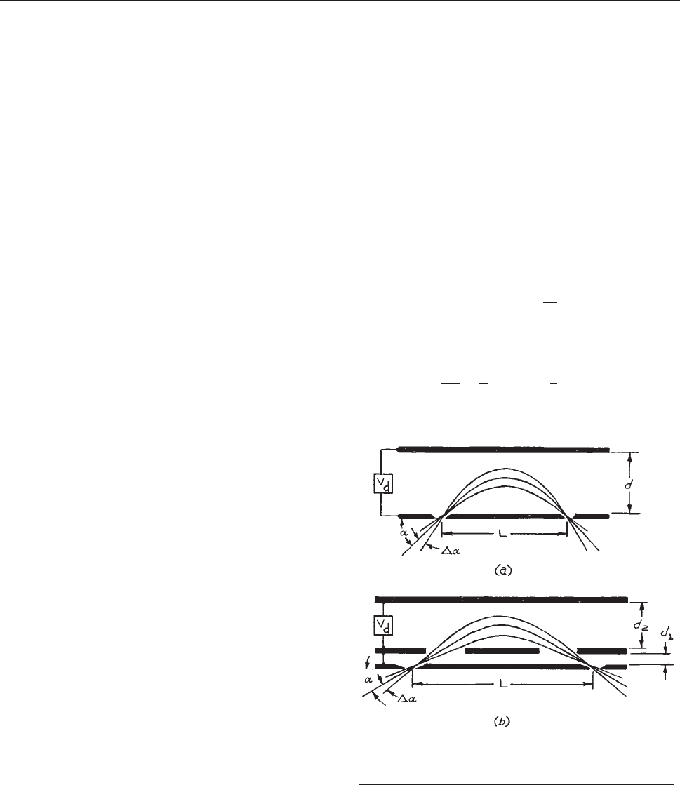
component of velo city normal to the retarding grid is
selected. There are also a number of practical difficulties.
The ratio of the initial energy to the energy at the potential
barrier varies rapidly for particles near the threshold for pen-
etrating the retarding barrier. This giv es rise to rapidly vary-
ing focusing effects near the threshold, so particles
approaching slightly off axis are often deflected away from
the collector. The result is that the transmission of the ana-
lyzer is unpredictable near the threshold. Another problem
with retarding-potential analyzers is that low-energy particles
near the retarding grid are seriou sly affected by space charge
and by stray electric and magnetic fields. Retarding potential
analyzers are very easily constructed and very compact, b ut
the vagaries of their performance suggests that their use for
high-resolution energy analysis be avoided if possible.
The energies of particles in a beam can be determined by
passing the beam through an electric or magnetic field, so
that the deflection of the particle paths is a function of the
particle energy per unit charge or momentum per unit
charge. In these dispersive-type analyzers, the shape of
the deflection field must be carefully controlled. Since it
is generally easier to produce a shaped electric field than
a shaped magnetic field, dispersive analyzers for particle
energies up to several keV are usually of the electrostatic
variety. For very high-energy particles, magnetic analyzers
are preferred, since production of the required electric fields
would demand inconveniently large electrical potentials.
The energy passband, DE, of an analyzer may be defined
as the full width at half maximum (FWHM) of the peak that
appears in a plot of transmitted current versus energy. Ideally
the transmission function is triangular. For a real analyzer it
resembles a Gaussian. W e shall take DE to be half the full
width of the transmission function; such an approximation
overestimates the passband of a real analyzer.
19
To first
order, entrance and exit slits or apertures, usually of equal
width w, establish the passband. The transmission function
also depends upon the maximum angular extent to which
particles can deviate from the central path leading from the
entrance to the exit slit. This angular deviation is defined by
angles Da in the plane of deflection and Db in the perpen-
dicular plane. If E is the central energy of particles trans-
mitted through an analyzer , then the resolution is:
DE
E
¼ aw þb DaðÞ
2
þc DbðÞ
2
ð5:83Þ
where a, b, and c are constants characteristic of the partic-
ular analyzer.
5.4.1 Parallel-Plate Analyzers
The simplest electrostatic analyzer employs a uniform
field created by placing a potential difference across a pair
of plane parallel plates, as shown in Figure 5.26. With the
entrance
and exit slits in one of the plates, first-order focus-
ing in the deflection plane is obtained when the angle of
incidence of entering particles is about a ¼ 45°.
The deflection potential V
d
(V), in relation to the inci-
dent energy E(eV), the plate spacing d, and the slit sepa-
ration L, is given by:
V
d
¼ E=qðÞ
2d
L
ð5:84Þ
with the proviso that d > L/2, to prevent particles from
striking the back plate. The resolution is:
DE
E
¼
w
L
þ DaðÞ
2
þ
1
2
DbðÞ
2
ð5:85Þ
Figure 5.26 Parallel-plate analyzers with (a) the
energy-resolving slits in one of the plates and (b) the slits in a
field-free region.
346 CHARGED-PARTICLE OPTICS
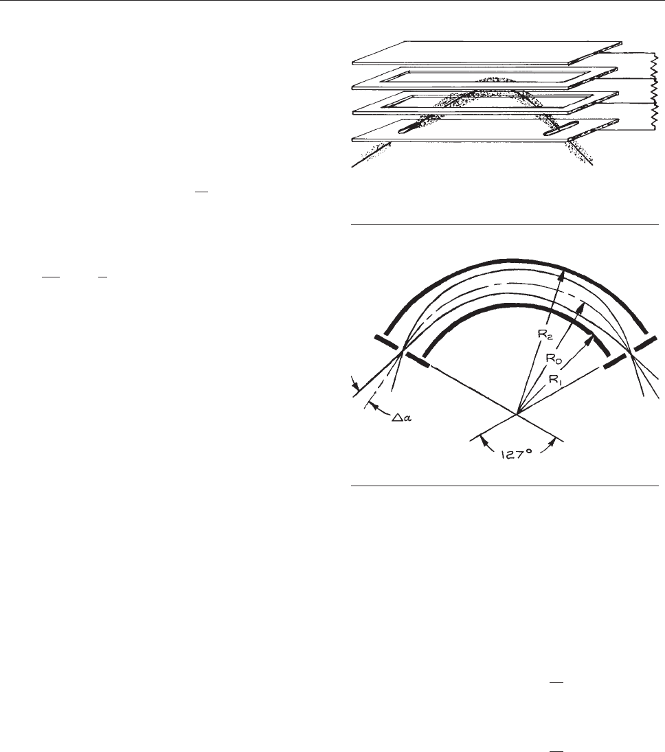
A point at the entrance aperture is focused into a line of
length 2
ffiffiffi
2
p
LDb, and the length of the exit slit is corre-
spondingly greater than that of the entrance slit.
When the slits are placed in a field-free region,
20
as in
Figure 5.26(b), optimum performance is obtained with the
angle
of incidence a ¼ 30°. The distance from the slits to
the entrance plate of the analyzer d
1
0:1d
2
, where d
2
is
the plate spacing. The deflection potential is:
V
d
¼ 2:6 E=qðÞ
d
2
L
ð5:86Þ
This arrangement gives second-order focusing in the plane
of deflection. The resolution is:
DE
E
¼ 1:5
w
L
þ 4:6 DaðÞ
2
þ 0:75 DbðÞ
2
ð5:87Þ
and the image of a point on the entrance slit is a line of
length 4LDb at the exit slit.
Although the parallel plate is an attracti ve design because
of its simple geometry, there are several problems. The
entrance apertures or slits in the front plate are at the boun-
dary of a strong field and act as lenses to produce unwanted
aberrations. This problem can be alleviated for the design
with the energy-resolving slits in a field-free region by
placing a fine wire mesh over these entrance apertures to
mend the field. A large electrical potential must be applied
to the back plate, creating a strong electrostatic field outside
the analyzer. The apparatus in which the analyzer is installed
must often be shielded from this field. In addition, because
the gap between the plates is large, the fringing field at the
edges of the plates can penetrate into the deflection region.
This problem can be solved by extending the edges of the
plate well beyond the deflection region, or by placing com-
pensating electrodes at the edges of the gap, as in Figure 5.27.
5.4.2 Cylindrical Analyzers
Two electrostatic analyzers employ cylindrical electrodes.
These are the radial cylindrical analyzer and the cylindri-
cal mirror analyzer.
The radial cylindrical analyzer is shown in Figure 5.28.
The
radial electric field is produced by an electrical poten-
tial placed across concentric cylindrical electrodes. Par-
ticles are injected midway between the electrodes in a
direction approximately tangent to the circular arc of
radius R
0
. First-order focusing is obtained if the cylindrical
electrodes subtend an angle of p=
ffiffiffi
2
p
¼ 127°. Assuming
a charged particle that originates at ground potential with
essentially no kinetic energy, and a mean pass energy E ¼
qV (that is, the energy of the particle that travels along
the central path of radius R
0
), the potentials to be applied
to the outer and inner cylindrical elements are:
V
outer
¼ V 1 2ln
R
2
R
0
ð5:88Þ
and
V
inner
¼ V 1 2ln
R
1
R
0
ð5:89Þ
Figure 5.27 Guard electrodes at the edges of a
parallel-plate analyzer to offset the distortion of the
field caused by fringing.
Figure 5.28 The radial cylindrical analyzer.
ENERGY ANALYZERS 347
where R
2
and R
1
are the radii of the outer and inn er
cylinders, respectively. The potentials on the electrodes
are such that a charged particle that enters at the mid-
radius R
0
with an energy equal to the pass energy E will
lose an amount of energy e qual to 2E ln R
2
/R
0
were it to
travel to the outer electrode, and would gain an amount
of energy equal to 2E ln R
0
/R
1
were it to travel to the
inner electrod e.
The resolution of this analyzer is:
DE
E
¼
w
R
0
þ
2
3
DaðÞ
2
þ
1
2
DbðÞ
2
ð5:90Þ
It is good practice to limit the angle of divergence in the
plane of deflection so that:
Da <
2
ffiffiffi
2
p
p
ðR
2
R
1
Þ
R
0
ð5:91Þ
in order to keep the filling factor below 50%. The radial-
field analyzer gives focusing only in the plane of deflec-
tion. A point at the entrance slit is imaged as a line of
length
ffiffiffi
2
p
pR
0
Db at the exit slit.
The cylindrical-mirro r analyzer is similar to the
parallel-plate analyzer except the deflection plates are
coaxial cylinders. In fact, the parallel-plate analyzer can
be considered a special case of the cylindrical mirror. In
the usual geometry, shown in Figure 5.29, the source is
lo
cated on the axis, and particles emitted into a cone defined
by polar angle a pass through an annular slot in the inner
cylinder. Particles of energy E are deflected so that they pass
through an exit slot and are focused to an image on the axis.
The cylindrical mirror is double-focusing (focusing occurs
in both the deflection plane and the perpendicular plane) so
that the image of a point at the source appears as a point at
the detector. An obvious advantage of this analyzer is that
particles at any azimuthal angle can be collected.
For optimum performance the entry angle a ¼ 42.3°,in
which case the distance from source to detector is L ¼
6.12R
1
.
21
The inner cylindrical plate is at the same poten-
tial as the source, and the potential on the outer cylinder,
relative to the inner cylinder, is:
V
outer
¼ 0:763 E=qðÞln
R
2
R
1
ð5:92Þ
It is wise to choose R
2
>2.5R
1
so that particles are
not scatte red from the outer electrode. The resolution
of the axial-focusing cylindrical-mirror analyzer is
approximately:
DE
E
¼ 1:09
w
L
ð5:93Þ
for a source of axial extent w and an energy-resolving
aperture of diameter w
0
¼ w sin a perpendicular to the axis
(as shown in Figure 5.29).
If
the source is not small and well defined, the entry
and exit slots in the inner cylinder can be used to
define the resolution of the cylindrical-mirror analyzer,
as in Figure 5.30; this arrangement is only first-
ord
er-focusing.
5.4.3 Spherical Analyzers
For many applications, the most desirable ana lyzer
geometry employs an inverse-square-law field cre ated
by placing a potential across a pair of concentric
spherical electrodes. Focusing in both the deflection
plane and the perpendicular plane can be obtained
using any sector portio n of a sphere. As shown in
Figure 5.31, the object and image lie on lines that are
Figure 5.29 Axial-focusing cylindrical-mirror analyzer.
Figure 5.30 Cylindrical-mirror analyzer with
energy-resolving slits in the inner electrode.
348 CHARGED-PARTICLE OPTICS
perpendicular to the entrance and exit planes, respec-
tively, and tangent to the circle described by the
midradius R
0
.Furthermore,byBarber’s rule, the object,
the center of curvature of the spheres, and the image lie
onacommonline.The180° spherical sector (Figure
5.
32) is often used because of the c ompact geometry
that
results from folding the beam back onto a line
parallel to its original path. As with the cylindrical
mirror, the spherical analyzer can be used to collect
all particles emitted from a point source at or near a
particular polar angle.
Assuming a charged particle that originates at ground
potential with essentially no kinetic energy, and a mean
pass energy E ¼qV (that is, the energy of the particle
that travels along the central path of radius R
0
), the
potentials to be applied to the outer and inner spherical
elements are:
V
outer
¼ V 2
R
0
R
2
1
ð5:94Þ
and:
Figure 5.32 The hemispherical analyzer: w is the width
of the entrance and exit apertures, Da the maximum
angular deviation of an incident trajectory, and w
m
the
maximum deviation of a trajectory from the central path
through the analyzer.
Figure 5.31 Focusing of a spherical analyzer.
ENERGY ANALYZERS 349

V
inner
¼ V 2
R
0
R
1
1
ð5:95Þ
where R
2
and R
1
are the radii of the outer and inner spheres,
respectively; in general, the potentials on the electrodes are
such that a charged particle that enters at the midradius R
0
with an energy equal to the pass energy E will lose an
amount of energy equal to 2E 1 R
0
/R
2
ðÞwere it to travel
to the outer electrode, and would gain an amount of energy
equal to 2ER
0
/R
1
1ðÞwere it to travel to the inner electrode.
The resolution of the 180° spherical sector (Figure 5.32)is:
DE
E
¼
w
2R
0
þ
1
2
DaðÞ
2
ð5:96Þ
and the maximum deviation, w
m
, of a trajectory from the
central path within the analyzer is given by:
w
m
R
0
¼
DE
E
þ Da þ
1
2Da
w
2R
0
þ
DE
E
2
ð5:97Þ
For the truncated spherical sector shown in Figure 5.31, the
resolution
is approximately:
DE
E
¼
w
R
0
ð1 cos /Þþsin /
ð5:98Þ
where / is the angle subtended by the analyzer sector and l
is the distance from the exit boundary of the analyzer to the
exit aperture. Although it would appear that the resolution
could be increased arbitrarily by increasing l, the aberra-
tions increase rapidly as the system becomes asymmetric.
It is best to employ the symmetric geometry with / in the
range 60–180°.
In comparison with the parallel-plate or cylindrical-mir-
ror analyzers, the spherical analyzer has the advantage of
requiring relatively low electrical potentials on the electro-
des. Because the electrodes are closely spaced in the spher-
ical analyzer, fringing fields are less of a problem and more
easily controlled. The chief drawback of this type of ana-
lyzer is the difficulty of fabrication and mounting.
5.4.4 Preretardation
In all electros tatic-deflection analyzers, the passband DE
is a linear function of the transmitted energy. Thus, the
absolute energy resolution of these devices can be
improved by retarding the inci dent particles prior to t heir
entering the a nalyzer. In principle, the passband of an
analyzer can be reduced arbitrarily by preretardation;
in practice, there are limitations on this technique. A
decelerating lens as in the example given in Section
5.
2.6 can slow charged particles incident on the entrance
aperture
of an analyzer. It would be very difficult, how-
ever, to design a lens system to be used with analyz ers
that have an annular entrance slit. Space charge and stray
electric and magnetic fields must be considered. Because
the flight path through an analyzer is long, it is usually
not possible to reduce the energy of transmitted particles
below about 2 eV before these effects result in severe
aberrations. Finally, it is important to recall that if
all particles of a particular energy in a b eam are to be
transmitted through an analyzer, the ratio of brightness
to energy must be conse rved (Section 5.1.3). As the
ener
gy of particles incident on an analyzer is decreased,
the current is ultimately reduced because the pencil
angle of the beam exceeds the acce ptance angle of the
analyzer.
When using a decelerating lens with an analyzer, it is
good prac tice to place an aperture on the high-energy
side of the lens and design the lens so that the image of
this aperture appears at the entrance plane of the ana-
lyzer. The need for a real entrance aperture is thereby
eliminated, and there are no metal surfaces in the vicinity of
the low-energy beam. Since space charge will cause the
low-energy beam to expand at the entrance plane of an
analyzer, current would be lost if a real entrance aperture
were used. As demonstrated by Kuyatt and Simpson,
space-charge expansion at a virtual aperture is compen-
sated by the spreading of the beam, with the result that
the beam appears to originate at an aperture of about the
same size as that in the absence of space charge
22
(see
Figure 5.16).
5.4.5 The Energy-Add Lens
An electrostatic energy analyzer can be used as a mono-
chromator to select the particles in a beam whose energies
fall within a narrow range, or as an analyzer to determine the
energy distribution of particles originating from a process
under study. In the latter application the passband of the
analyzer must be scanned over the energy range of interest.
350 CHARGED-PARTICLE OPTICS

Scanning can be accomplished by varying the potential dif-
ference between the analyzer electrodes; however, neither
the transmission nor the energy resolution will be constant.
A more satisfactory method for determining the energy dis-
tribution of particles in a beam is to fix the analyzer poten-
tial at the voltage that allows transmission of particles of the
highest desired energy and preaccelerate the incident par-
ticles by a variable amount. The energy that must be added
to the particles so that they pass through the analyzer is then
a measure of the difference between their initial energy and
the energy necessary to transmit them with no preaccelera-
tion. In a scattering experiment, for example, the analyzer
might be set to transmit elastically-scattered particles, and
the distribution of energy lost by inelastically scattered par-
ticles would be scanned by monitoring the transmitted cur-
rent as a function of energy added.
An energy-add lens must add back energy without dis-
turbing the optics of the analyzer. Kuyatt
23
showed that the
electron-optical analog of the field lens is suited to this
application. This lens is positioned so that its first principal
plane coincides with the particle source to be examined.
The source is then imaged onto the second principal plane
with unit magnification. For a reasonably strong lens (V
2
/V
1
> 3), the position of the principal planes is nearly independ-
ent of the voltage ratio and the separation of the planes is
small. Thus particles from the source can be accelerated by
a variable amount without changing the apparent position
of the source. An energy-add lens used in conjunction with
a fixed-ratio decelerating lens for preretardation at the input
of an electron energy analyzer is schematically illustrated
in Figure 5.33. For transmission of electrons with energy A
(eV
) less than the maximum energy to be transmitted, the
Figure 5.33 An energy-add lens and fixed-ratio retarding lens at the input of an analyzer.
The energies and corresponding lens voltages for electrons transmitted with no added
energy are given above the lens. Energies and voltages for transmission of electrons that
have lost energy A are shown below. The ‘‘source’’ is defined by an aperture that is finally
imaged at the entrance plane of the analyzer.
ENERGY ANALYZERS 351

potential of the second element of the energy-add lens and
every electrode thereafter is increased by A (V). For a
positive ion analyzer, the potential would be decreased by
A/n (V), where n is the charge state of the ions.
A problem with the energy-add lens is that the object pupil
moves as the lens voltages change. Thus, while the apparent
source remains stationary, the beam angle may v ary over a
considerable range as the lens is tuned. As a result, the lenses
following the energy-add lens may be overfi lled. This can be
avoided by placing a second field lens downstream from the
first at an intermediate image of the apparent source. The
second field lens is then tuned to gi v e a zero beam angle. An
einzel lens (Section 5.2.2) can be used so that there is no net
change
of energy as the beam angle is manipulated.
5.4.6 Fringing-Field Correction
For the radial-field cylindrical analyzer or the spherical ana-
lyzer, particles must pass through the fringing field at the
edge of the electrode gap as they enter the deflection region.
The electric field at the edge bulges out of the gap, and this
curvature produces a focusing effect that causes undesirable
aberrations. Herzog
24
and Wollnik and Ewald
25
have shown
that a diaphragm at the entrance of the condenser gap can
largely eliminate this problem. As illustrated in Figure 5.34,
th
e diaphragm, when properly located, produces a field that
has the same effect as a field abruptly terminated at a dis-
tance d* in front of the condenser gap. The appropriate
location of the diaphragm as a function of the dimensions
given in Figure 5.34 can be determined for either a thick or
th
in diaphragm from the graphs in Figure 5.35.
Figure 5.34 A shielding diaphragm to correct for focusing
at the fringing field at the edge of an electrostatic
condenser. The field appears as if it were terminated
abruptly at a distance d* from the gap.
Figure 5.35 The distance of the apparent field boundary
from the edge of the condenser electrodes as a function of
the dimensions given in Figure 5.34 for (a) a thick
diaphragm
and (b) a thin diaphragm. (From H. Wollnik and
H. Ewald, ‘‘The Influence of Magnetic and Electric Fringing
Fields on the Trajectories of Charged Particles,’’ Nucl. Instr.
Meth., 36, 93 (1965); by permission of North-Holland
Publishing Company.)
352 CHARGED-PARTICLE OPTICS
5.4.7 Magnetic Energy Analyzers
Magnetic fields are employed in se veral charged-particle-
energy analyzers and filters. The trochoidal analyzer
[Figure 5.36(a)] has proven quite useful for the dispersion
of
very-lo w-ener gy (0 to 10 eV) electrons and ions. This
device employs a magnetic field aligned with the direction of
the charged-particle beam, and an electric field perpendicu-
lar to this direction.
26
The trajectory of a particle injected
into this analyzer describes a spiral and the guiding center of
the spiral drifts in the remaining perpendicular direction. The
drift rate depends upon the particle energy; a beam entering
the device is dispersed in energy at the exit. The projection of
the trajectory on a plane perpendicular to the electric field
direction is a trochoid, hence the name. The de vice requires a
very uniform magnetic field of about 100 gauss. The field is
usually produced by a relatively large Helmholtz pair (see
Section 5.6.5) mounted outside the vacuum system contain-
ing
the analyzer. The result is that the entire experiment is
immersed in the field. This may be a drawback in some
cases, but, on the other hand, for low-energy electrons or
ions, the field helps contain particles that otherwise would be
lost from coulombic repulsion (i.e., space charge).
The Wien filter [Figure 5.36(b)] similarly employs crossed
electric
and magnetic fields, howev er , the fields are perpendic-
ular to one another and both are perpendicular to the injected
beam direction.
27
The Coulomb force induced by the electric
field E deflects charged particles in one direction and the
Lorentz force associated with the magnetic field B tends to
deflect them in the opposite direction. The forces balance for
one velocity , v ¼ |E|/|B|, and particles of the corresponding
energy are transmitted straight through to the exit aperture.
A magnetic field alone, perpendicular to the direction of
a charged-particle beam will provide energy dispersion,
provided that the particles are all of the same mass and
charge [Figure 5.36(c)]. Sector magnets such as those used
in
mass spectrometers are used in electron spectro-
meters for very-high-energy electrons and ions, the advant-
age over electrostatic deflectors being that large electrical
potentials are not required. Another advantage is that the
deflection is in the direction parallel to the magnet pole
face, making it possible to view the entire dispersed spec-
trum at one time. In contrast, energy dispersion in an
electrostatic device results in a significant portion of the
dispersed particles striking one or the other electrode.
Figure 5.36 Charged-particle energy analyzers with
magnetic fields: (a) the trochoidal analyzer with an
electromagnet; (b) the Wien filter; (c) the sector
magnet analyzer. Trajectories for electrons of differ ent
energies are shown. Magnet polarities are for electrons.
ENERGY ANALYZERS 353
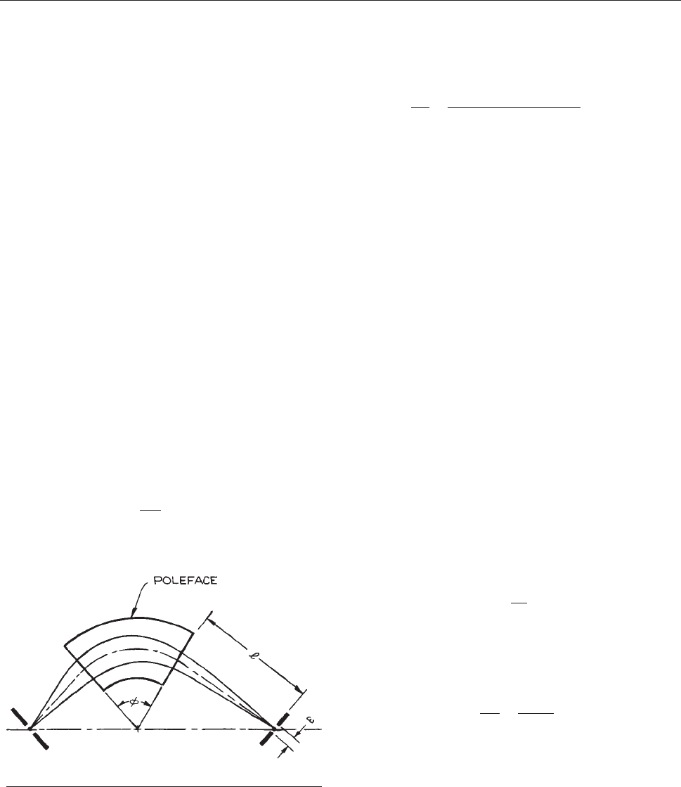
5.5 MASS ANALYZERS
Mass analysis is more complicated than energy analysis of
an isotopically pure beam, since energy and momentum
are independent variables in a mixed beam. A detailed
discussion of the many types of mass analyzers that have
been developed is beyond the scope of this book. The
principles of operation of a few representative analyzers
will be described.
5.5.1 Magnetic Sector Mass Analyzers
The deflection of ions in a perpendicular magnetic field is
proportional to the particle momentum per unit charge. If
all particles entering a magnetic field have the same
energy per unit charge, then the field will separate par-
ticles according to their masses. In the usual c onfigura-
tion, a magnetic field is produced between the two
parallel, sector-shaped polefaces of an electromagnet,
as illustrat ed in Figure 5.37. The focusing properties of
this
field
28
are the same as those of the spherical electro-
static analyzer, a nd the locations of the e ntrance and exit
slits are given by Barber’s rule (Section 5.4.3). The
radiu
s of curvature of ions of energy E in a magnetic
field of intensity B is:
R ¼
144
Bn
ffiffiffiffiffiffiffi
mE
p
cm ð5:99Þ
with B in gauss, E in eV, m in amu, and n the charge state.
In terms of the parameters specified in Figure 5.37, the
resolution
is:
DE
E
¼
w
R
0
1 cos /ðÞþ‘ sin /
ð5:100Þ
where R
0
is the radius of curvature of the central trajec-
tory. To first order, there is no focusing in the plane
perpendicular to the plane of deflection. When the cur-
vature of the fringing field is taken into consi deration,
however, so me focusing in the perpendicula r plane
results. Incident ion trajectories should be normal to
the entrance pla ne to avoid focusing e ffects.
5.5.2 Wien Filter
The W ien filter , employing mutually perpendicular electric
andmagneticfieldsnormaltotheiontrajectory[Figure
5
.36(b)] can serve to disperse char ged particles according
to
either mass or energy.
27
Ions of a unique velocity v will
experience equal and opposite forces through interaction
with the two fields (the Coulomb force and the Lorentz
force) and be transmitted in a straight line. If all of the ions
injected into the fields of the Wien filter ha v e the same
kinetic energy, ions of a unique mass are transmitted straight
through; if the injected ions have all been accelerated
through the same potential (relativ e to their source), ions
of a unique mass-to-charge ratio are transmitted. In most
W ien filters a pair of permanent magnets supplies the mag-
netic field, and the electric field is produced by placing an
electrical potential V
d
across a pair of parallel electrodes
separated by a distance d. The velocity of ions transmitted
straight through the Wien filter is
v ¼ 10
8
V
d
dB
cm s
1
ð5:101Þ
with V
d
in volts, d in cm, and B in gauss. Varying V
d
scans
the mass spectrum of ions. If slits of width w are placed at
the entrance and exit of a Wien filter of length L, the mass
resolution for ions of energy E is:
Dm
m
¼
2dEw
qV
d
L
2
ð5:102Þ
assuming the incident ion trajectories are normal to the
entrance plane. Boersch, Geiger, and Stickel have made a
detailed analysis of the focusing properties of the Wien filter.
29
Figure 5.37 Focusing of the magnetic sector.
354 CHARGED-PARTICLE OPTICS
5.5.3 Dynamic Mass Spectrometers
Dynamic mass spectrometers use time-varying electric or
magnetic fields or timing circuits to disperse ions accord-
ing to their masses.
30
The quadrupole mass analyzer and
the linear time-of-flight mass spectrometer are the two
most successful designs of this type.
The quadrupole mass analyzer illustrated in Figure 5.38
employs a time-v arying electric quadrupole field. For a par-
ticular
field intensity and frequency, only ions of a unique
mass-to-charge ratio will follow a stable path and pass
through the field. As shown in the figure, the quadrupole
field is approximated by a square array of four cylindrical
electrodes parallel to the axis along which ions are injected.
The potential applied to the vertical pair of electrodes is:
V
v
¼ U þ V cos 2pft ð5:103Þ
while for the horizontal pair
V
h
¼U þV cos 2pft þpðÞ ð5:104Þ
where f refers to an r.f. frequency. For optimum perform-
ance the ratio of the d.c. field to the r.f. field is adjusted so
that U/V 0.17. For singly charged ions, the mass of the
ions that are transmitted is:
m ¼ 0:14
V
r
2
f
2
amu ð5:105Þ
with V in volts, r in cm, and f in MHz. Mass scanning is
usually accomplished by varying the r.f. amplitude V, while
fixing the ratio of d.c.-to-r.f. voltage (U/V) and the fre-
quency (f). Quadrupole analyzers are compact and offer
the advantages of high transmission, fast scanning, and
insensitivity to the initial ion energy. These instruments
are available commercially as residual-gas analyzers for
high-vacuum systems and are suitable for use in many
scattering experiments.
The time-of-flight mass spectrometer depends upon the
fact that the velocity of ions of the same kinetic energy is a
function of mass. In this spectrometer, positive (negative)
ions that have been accelerated to an energy of about 1 keV
are admitted to a long drift tube in short bursts by a
negative (positive) electrical pulse applied to a grid at
the entrance of the drift region. The lightest ions travel
most rapidly and are the first to arrive at the detector
located at the end of the drift tube. Heavier ions arrive in
the order of their masses. The obvious advantage of this
design is that the entire mass spectrum is scanned in a few
microseconds. Furthermore, the spectrum can be scanned
thousands of times each second, making this system ideal
for studying rapidly varying processes. Its chief drawback
is its size, since the length of the flight tube required
to achieve good resolution may be greater than a meter.
5.6 ELECTRON- AND ION-BEAM
DEVICES: CONSTRUCTION
To realize the design of a charged-particle optical system,
it is necessary to create an environment where a stream of
particles can travel without loss of momentum and to make
electrodes and pole pieces that faithfully produce the elec-
trical and magnetic fields necessary to deflect the particles.
5.6.1 Vacuum Requirements
Charged particles lose energy through interactions with
gas molecules; thus ions or electrons can only be trans-
ported in a vacuum. The required pressure depends upon
the distance they must travel. As noted in Section 3.1.2, the
mean
free path at a pressure of 1 mtorr is a few centimeters,
while at 10
5
torr this increases to a few meters. It follows
that high vacuum is required for the operation of a
charged-particle optical system.
Figure 5.38 The quadrupole mass analyzer.
ELECTRON- AND ION-BEAM DEVICES 355

Conducting surfaces must be kept clean, since contamina-
tion with an insulating material will result in the buildup of
surface charges that cause an unpredictable deflection of
charged particles passing nearby . Clean electrode surfaces are
particularly important for particles of energy less than 100 eV
and when high spatial resolution is required. All electrodes
must be clean and free of hydrocarbon contamination before
installation in the vacuum system (Section 3.6.3). An oil-free
v
acuum system with turbomolecular pumps, ion pumps, or
sorption pumps (Section 3.4.3) is most desirable, although a
system
ev acuated with a properly trapped oil diffusion pump
(Sections 3.5.5 and 3.4.2) is adequate in many cases.
Polyphen
yl ether diffusion-pump fluids such as Con v alex-
10 (Consolidated Vacuum) or Neo v ac Sy (Varian) have been
found to be the least offensiv e diffusio n-pump oils for electron-
optical syste ms. In lo w-energy-beam de vices, a daily bake to
200–300 ° C will keep electrode surfaces clean and ensure
stable operation. Hydrocarbons on aperture surfaces exposed
to charged particles create a particularly obnoxious problem.
Bombardment of the adsorbed hydrocarbons produces an insu-
lating carbon polymer that adheres tenaciously to the under-
lyingmetal.Thiscarbonmaterialcanonlyberemovedby
high-temperature baking (400° C), by vigorous application
of an abrasi ve, or by etching with a strong solution of NaOH.
When baking is impractical, electrode surface quality and
stability are often impro v ed by a coating of carbon black. A
surface can be blacked by brushing with a sooty acetylene
flame; howe v er, the coating produced in this manner does not
adhere well. A superior coating can be produced by spraying
or brushing the surface with a thin water or ethanol slurry of
colloidal graphite (Aquadag, made by Acheson Colloids Co.).
The tenacity of this coating is improved by preheating the
metal surface to about 100 °C before the slurry is applied.
5.6.2 Materials
The materials used to construct lens elements must be such
that the equipotential surfaces near the electrodes faithfully
follow the contours of the electrode surfaces. These surfaces
must be clean, and must withstand periodic cleansing by bak-
ing, bead blasting, electropolishing, or harsh chemical action.
The refractory metals such as tungsten, tantalum, and
particularly molybdenum are probably the best electrode
materials. These metals have a low, uniform, surface poten-
tial, they do not oxidize at ordinary temperatures, and they
are bakeable. Refractory metals are hard and rather brittle.
Only the wrought material can be machined or formed
easily. Stock produced by sintering is very difficult to
machine. Electrodes spun from sheet molybdenum are
available in cylindrical and spherical shapes (Bomco, Inc.).
Oxygen-free high-conducti vity (OFHC) copper (Section
1.
3.3) is often used for electrode fabrication, although Kuyatt
used
commercial, half-hard copper in some applications.
Exposed to air , copper forms a surface oxide, but this oxide
is conducting. Copper is bakeable and reasonably machinable.
Stainless steels (Section 1.3.1) contain domains of differ-
ent
composition, some of which may be ferromagnetic. The
magnetic properties of stainless steels vary considerably,
even between samples of the same net composition; these
materials are unsuitable for use with low-energy charged
particles unless they are carefully annealed to remove resid-
ual magnetism (Section 1.3.1). Stainless steels have the
adv
antage of being bakeable, strong, and easy to machine.
Aluminum (Section 1.3.4) is unsuitable, because its sur-
face
is rapidly attacked by oxygen in the air to form a hard,
insulting, layer of oxide. On the other hand, aluminum has
a low density, and most aluminum alloys are easy to
machine or form by bending, spinning, or rolling. When
these properties are important, the surface can be plated
with copper or gold to overcome the problem of oxidation.
Electrodes and lenses must be mounted on nonconducting
materials. Glass or ceramic (Section 1.3.7) or, in some cases,
plastic
(Section 1.3.6) can be used for this purpose. Of the
c
eramic materials, alumina is the best insulator and the stron-
gest. Precision-ground rods and balls are av ai lable commer-
cially. Alumina circuit board substrate in the form of thin
plates laser-cut in complex shapes can be obtained quite inex-
pensiv ely. There are also machinable ceramics from which
complicated shapes can be formed (MACOR from Corning).
As noted in Chapter 3, it is important to be aware that the
resistivity of a ceramic is strongly dependent upon temper-
ature. The resistivity of a ceramic material falls by roughly
a factor of 10 for ev ery 100 ° C increase in temperature.
31
For example, the resisti vity of alumina is greater than 10
17
ohm cm at 100 ° C and falls belo w 10
7
ohm cm at 1000 ° C.
Plastics are machinable and inexpensive. Unfortunately,
they are not bakeable; a further disadvantage is that they
contain hydrocarbons that can contaminate the vacuum
environment. Polyimide plastic sheet (Kapton) is a useful
insulator.
356 CHARGED-PARTICLE OPTICS
Mica in sheets is an excellent insulator (‘‘stove mica’’
from Spruce Pine Mica Co.).
5.6.3 Lens and Lens-Mount Design
Most electron-optical lenses are created by the fields in the
gap between coaxial cylindrically symmetric electrodes.
These electrodes must be designed so that electric fields
associated with the lens mounts and the vacuum-container
walls do not penetrate the gap between electrodes. The
involuted design illustrated in Figure 5.39 ensures that
the
lens gap is shielded. The step on the shoulder of the
lens elements is designed so that the inner gap is of the
correct size when the outer gap is adjusted to some stand-
ard width. In this way all the lenses in a system can be
correctly positioned with the aid of a single gauge.
There are two widely used, semikinematic schemes for
mounting lens elements. These are the rod mount and the
ball mount, illustrated in Figures 5.40 and 5.41, respectiv ely.
In
the rod mount, cylindrical lens elements rest on ceramic
rods that insulate the elements from one another and from
a grounded mounting plate. The critical dimensions are
the diameters of the lens elements and the width of the
channel in which the rods rest. In order for the lens element s
to be coaxial, their outer diameters must be identical. This
requirement is met by making all of the elements from a
single piece of rod stock that has been carefully turned to a
uniform diameter. To ensure that the elements are mounted
coaxially, it is then only necessary that the sides of the
Figure 5.39 Tube lens electrodes are constructed so that
external fields cannot penetrate the lens gap. When
mounting the lens elements, a gauge is inserted to ensure
correct spacing at the invisible lens gap.
Figure 5.40 Cylindrical lens elements mounted on ceramic
rods.
Figure 5.41 Lens elements mounted on ceramic balls.
ELECTRON- AND ION-BEAM DEVICES 357

channel in which the rods rest be parallel. This is easily
accomplished in a milling operation. If the ver ti cal position
of the lens axis is important, then the width of the channel
becomes a critical dimension. Of course, the diameter of the
rods is important, but, as noted elsewhere (Section 1.3.7),
alumina
rod, centerless-ground to high precision, is commer-
cially available. For maximum strength the rods should be
about 90° apart around the circumference of the lens element.
In the ball-mounting scheme, lens elements are insulated
from one another and positioned by ceramic balls that rest in
holes near the edges of the lenses. This system is preferred
when mounting very thin elements, as in an aperture-lens
system. Ideally only three balls should be used. The critical
dimensions are the locations of the holes and their diameter .
The holes should be bored, or drilled and reamed, in a milling
machine or jig borer using a dividing head or a precision
rotary table. For balls of diameter d, the hole diameter should
be d sin 45°, in which case the spacing between lens elements
will be d cos 45°. A lens system is assembled by stacking lens
elements alternating with balls. The stack must be clamped.
The clamp should hav e some spring and should bear on the
topmost element only at one or two points near the center of
the circle around which the balls are located. A rigid clamp
will tend to drive the balls into their holes and may crush the
edges of the holes. If the clamp bears too near the edge, there
is a danger that the stack may become cocked off axis.
5.6.4 Charged-Particle Detection
For particle energies up to a few tens of keV, a stream of
charged particles of sufficient intensity can be collected
and measured directly as an electrical current. To achieve
the greatest sensitivity, individual ions or electrons can be
detected with an electron multiplier. Charged particles can
also be detected with photographic emulsions, scintilla-
tors, and various solid-state devices. Emulsions and scin-
tillators have largely been supplanted by the methods
mentioned above, and solid-state devices (Section 7.9.1)
are
only suitable for the detection of high-energy particles
(above 30 keV).
The collector for the direct detection of a current of
charged particles is called a Faraday cup. Typical designs
are illustrated in Figure 7.35. These simple collectors are
c
onnected directly to a current-measuring device and are
useful at currents down to the detection limits of modern
electrometers about 10
14
A. Their design and use is dis-
cussed in Section 7.9.
Single
charged particles can be detected with electron
multipliers. Their use and application is discussed in
Section 7.9.
5.6.5 Magnetic-Field Control
A magnetic field may cause aberrations in a char ged-particle
optical system. The Earth’s magnetic field is the usual source
of problems, but large concentrations of magnetic materials
nearby or large currents, such as those associated with a cyclo-
tron, may also produce magnetic fields of sufficient intensity
to deflect the trajectories of electrons or ions in an optical
system. The Earth’ s magnetic field is about 0.6 gauss directed
at an angle of elev ation in the north–south plane roughly equal
to the local latitude. Whether or not this is a problem depends
on the energy and mass of the transmitted charged particles,
and the dimensions of lens elements and apertures through
which the particles must pass. For example, the radius of
curvature of the path of a 10 eV electron moving perpendic-
ular to the Earth’ s field is 15 cm; this amounts to a defection of
1.5 mm along a 1 cm path. For a low-energy (<100 eV)
electron spectrometer , such considerations may lead to a
residual-field tolerance of less than 1 milligauss.
There are two methods to eliminate magnetic fields: an
opposing field can be applied to cancel the offending field
throughout the volume occupied by the apparatus, or the
apparatus can be enclosed in a shield of high permeability
ferromagnetic metal that shunt s the local field around the
enclosure. An electromagnet constructed to make an oppos-
ing field is the less expensive, but also the more ungainly,
approach; the dimensions of the coils may exceed by a factor
of 10 the dimensions of the apparatus to be shielded. In addi-
tion, without an elaborate feedback control, an electromagnet
can only cancel a constant (dipole) fi eld. A magnetic shield
need be only large enough to contain the apparatus, but the
construction requires expensiv e fabrication and heat treat-
ment of the shielding alloy that is itself relatively expensi v e.
Electromagnets for canceling the ambient field are
assembled from two or more pairs of current-carrying loops.
A continuous solenoid would be impractical, since access
to the interior volume is limited. Caprari has surveyed opti-
mal geometries for a range of possibilities.
35
The most
common arrangement consists of a pair of identical circular
358 CHARGED-PARTICLE OPTICS
magnet coils spaced apart by half the coil diameter. These
are referred to as Helmholtz pairs or Helmholtz coils.The
axis of the pair of coils must be oriented parallel to the field
that is to be canceled. Alternatively, three pairs arranged
orthogonally can be used with the current to each adjusted
to give a net field that opposes the offending field. The
Helmholtz coil geometry is illustrated in Figure 5.42.The
fi
eld along the axis of a round Helmholtz pair, a distance z
above the bottom coil is given by:
B ¼ 0:32
NI
R
1 þ
z
R
2
3=2
þ 1 þ 1
z
R
2
3=2
()
gauss
ð5:106Þ
where N is the total number of turns, I is in amperes, and R
and Z are in cm. For square coils, a similar expression with R
replaced by L/2 applies. The orientation of the coils and the
exact value of the current must be determined with the aid of
a magnetometer. The field produced by a Helmholtz pair is
of high uniformity only in a small volume midway between
the coils and near the axis. For example, a uniformity
of 0.1% is achieved in a central volume of 2 3 10
2
cubic radii, a uniformity of 1% in a volume of 1.5 310
1
cubic radii, and a uniformity of 5% in a volume of 0.6 cubic
radii.
34
Thus, the coil dimensions must exceed those of the
apparatus to be shielded by at least a factor of 10 in order to
reduce the magnetic field to a few milligauss. In addition, it
is important to recognize that a Helmholtz coil can only
cancel the dipole component of the ambient field.
Shielding electron-optical devices from ambient magnetic
fields can be accomplished with an enclosure fabricated of
special high-permeab ility nickel–iron alloys.
36
These materi-
als are availab le as sheet or tubing and thus as a practical
matter are best formed into simple cylindrical shapes, either
with or without endcaps, depending on requirements of access
to the interior. Construction details are important in determin-
ing the performance of a magnetic shield. Removable parti-
tions and endcaps should be designed to overlap the fixed
pieces to which they are attached and they should fit tightly.
Permanent joints should be spot-welded lap joints or arc-
welded butt joints. Magnetic-shielding alloys only attain their
high permeability after annealing in a hydrogen atmosphere
follow ing a precisely defi ned tempera ture schedule. Mechan-
ical stress degrades the permeability of the material so the
annealing is carried out after fabrication. It usually makes
sense to have a shield fabricated by a shop that is prepared
to do the annealing. Suppliers and fabricators of magnetic-
shielding mater ials include Amuneal Corp., Magnetic Metals
Co., and the Magnetic Shield Division of Perfection Mica Co.
A magnetic shield must be handled carefully. Bending or
sharp blows degrade the shielding properties, as will contact
with magnetic materials; magnetized tools are frequently the
culprits. The annealed material should not be heated above
400 °C. It must be emphasized that magnetic shielding cannot
be accomplished casually; a few sheets of ‘‘l-metal’’ wrapped
around a v acuum system will often do more harm than good.
The performance of a magnetic shield is specified by an
attenuation factor, A, given by the ratio of the magnetic field
H
0
at a point in the absence of the shield to the field strength
H
s
at the same point when it is surrounded by the shield:
A ¼
H
0
H
s
ð5:107Þ
Figure 5.42 Round and square Helmholtz coils.
ELECTRON- AND ION-BEAM DEVICES 359

The calculation of the attenuation factor is generally dif-
ficult, howev er, since a shield is usually constructed of sheet
and tubing, a reasonable estimation can be made from
approximations to the attenuation factor for simple geomet-
ric shapes. The attenuation of a long cylindrical shield can be
approximated as that for an infinitely long cylinder and the
attenuation of a closed box can be approximated as that for a
sphere. The attenuation factor depends upon the thickness of
the shielding material, the overall dimensions of the shield,
and l, the permeability of the shielding material. Low-
saturation alloys used to shield fields of the order of 1 gauss
have permeabilities of about 40 000. From the formulae
below it will be obvious that two or more nested shields of
thin material are much preferable to a single thick shield.
37
For a long cylinder, the attenuation factor is given
approximately by:
A
ld
2R
ð5:108Þ
and for a sphere by
A
2ld
3R
ð5:109Þ
where R is the radius of the cylinder or sphere and d is the
thickness of the material. For a nested pair of cylinders or
spheres of radius R
1
and R
2
spaced apart by a distance
D ¼jR
1
R
2
j, the attenuation factor:
A A
1
A
2
2D
R
ð5:110Þ
where A
1
and A
2
are the attenuation factors for each of the
cylinders or each of the spheres alone and R is the mean
radius of the two. Note that the attenuation increases with
the spacing between the two shields.
A sample calculation illustrates the advantage of multiple
shields: A single cylindrical shield, 20 cm in diameter of 1
mm thick material with a permeability of 40 000 gives an
attenuation factor of 200. Nested shields 20 cm and 22 cm in
diameter of the same material giv e an attenuation factor of
7000; for shielding from the Earth’ s magnetic field, the dou-
ble shield reduces the field well into the sub milligauss range.
An opening in a magnetic shield is often unavoidable. For
example a shield surrounding a vacuum system must be left
open at one end for attachment of the pump and for electrical
and mechanical feedthroughs. The external field penetrates
into the opening. The attenuation near an opening reaches a
value of about two-thirds of the maximum attenuation of the
shield at a distance into the shield volume about equal to the
mean radius of the opening.
38
A skirt of shielding alloy
extending outward from an opening, thus effectively dis-
placing the opening outward from the shielded volume,
helps to alleviate the problem.
Cited References
1. K. R. Spangenberg, Vacuum Tubes, McGraw-Hill, New
York, 1948.
2. J. R. Pierce, Theory and Design of Electron Beams , 2nd edn.,
Van Nostrand, New York, 1954.
3. O. Klemperer and M. E. Barnett, Electron Optics, 3rd edn.,
Cambridge University Press, Cambridge, 1971.
4. V. E. Cosslett, Introduction to Electron Optics, Oxford
University Press, Oxford, 1946.
5. D. Roy and J. D. Carette Electron Spectroscopy, H. Ibach,
(Ed.), Topics in Current Physics, Springer, Berlin, 1977,
Chapter 2.
6. V. W. Hughes and H. L. Schultz (Eds.), Methods of Exper-
imental Physics, Vol. 4A, Atomic Sources and Detectors
Academic Press, New York, 1967.
7. E. Harting and F. H. Read, Electrostatic Lenses, Elsevier,
New York, 1976.
8. F . H. Read, J. Phys., E2, 165, 1969; (b) F. H. Read, J. Phys., E2,
679, 1969; (c) F. H. Read, A. Adams, and J. R. Soto-Montiel, J.
Phys., E4, 625, 1971; (d) A. Adams and F . H. Read, J. Phys., E5,
150, 1972; (e) A. Adams and F. H. Read, J. Phys., E5, 156, 1972.
9. S. Natali, D. DiChio, E. Uva, and C. E. Kuyatt, Rev. Sci.
Instr., 43, 80, 1972; D. DiChio, S. V. Natali, and C. E. Kuyatt,
Rev. Sci. Instr., 45, 559, 1974.
10. D. W. O. Heddle, Tables of Focal Properties of Three-
Element Electrostatic Cylinder Lenses, J.I.L.A. Report No.
104, University of Colorado, Boulder, 1970.
11. R. E. Collins, B. B. Aubrey, P. N. Eisner, and R. J. Celotta,
Rev. Sci. Instr., 41, 1403, 1970.
12. D. DiChio, S.V. Natali, C. E. Kuyatt, and A. Galejs, Rev. Sci.
Instr., 45, 566, 1974.
13. J. A. Simpson, in Methods of Experimental Physics, Vol. 4A,
V. W. Hughes and H. L. Schultz (Eds.), Academic Press, New
York, 1967, Section 1.15.
14. An estimation of image expansion at the space-charge limit
can be obtained from the data of W. Glaser, Grundlagen der
Elektronenoptik, Springer, Vienna, 1952, p. 75.
15. R. G. Wilson and G. R. Brewer, Ion Beams, Wiley, New
York, 1973.
360 CHARGED-PARTICLE OPTICS

16. C. D. Moak, H. E. Banta, J. N. Thurston, J. W. Johnson, and
R.F. King, Rev. Sci. Instr., 30, 694, 1959; M. von Ardenne,
Tabellen der Electronenghysit IonengRysik und Ubermilros-
kopie, Deutscher Verlag der Wissenschaften, Berlin, 1956.
17. W. Aberth and J. R. Peterson, Rev. Sci. Instr., 38, 745, 1967.
18. J. A. Simpson, Rev. Sci. Instr., 32, 1283, 1961.
19. M. E. Rudd Low Energy Electron Spectrometry,byK.D.
Sevier (Ed.), Wiley-Interscience, New York, 1972, Chapter
2, Section 3; A. Poulin and D. Roy, J. Phys., E11, 35, 1978.
20. T. S. Green and G. A. Proca, Rev. Sci. Instr., 41, 1409, 1970; G.
A. Proca and T. S. Green, Rev. Sci. Instr., 41, 1778, 1970.
21. V. V. Zashkvara, M. I. Korsunskii, and O. S. Kosmachev,
Soviet Phys. Tech. Phys., 11, 96, 1966; H. Sar-el, Rev. Sci.
Instr., 38, 1210, 1967, and 39, 533, 1968; J. S. Risley, Rev.
Sci. Instr., 43, 95, 1972.
22. C. E. Kuyatt and J. A. Simpson, Rev. Sci. Instr., 38, 103, 1967.
23. C. E. Kuyatt, unpublished lecture notes; see also A. J.
Williams, III, and J. P. Doering, J. Chem. Phys., 51, 2859,
1969; J. H. Moore, J. Chem. Phys., 55, 2760, 1971.
24. R. F. Herzog, Z. Phys., 89, 447, 1934; 97, 596, 1935; Phys.
Z., 41, 18, 1940.
25. H. Wollnik and H. Ewald, Nucl. Instr. Meth., 36, 93, 1965.
26. A. Stamatovic and G. J. Schulz, Rev. Sci. Instr., 39, 1752,
1968; A. Stamatovic and G. J. Schulz, Rev. Sci. Instr., 41,
423, 1970: L. Sanche and G. J. Schulz, Phys. Rev. A, 5
, 1672,
1972;
D. Roy, Rev. Sci. Instr., 43, 535, 1972.
27. R. L. Seliger, J. Appl. Phys., 43, 2352, 1972.
28. E. Segre, Experimental Nuclear Physics, Vol. 1, Wiley,
New York, 1953, part V.
29. H. Boersch, J. Geiger, and W. Stickel, Z. Phys., 180,415,
1964.
30. E. W. Blauth, Dynamic Mass Spectrometers, Elsevier,
Amsterdam, 1966; P. H. Dawson, Quadrupole Mass
Spectrometer, Elsevier, Amsterdam, 1976.
31. W. D. Kingery, H. K. Bowen, and D. R. Uhlmann,
Introduction to Ceramics, 2nd edn., John Wiley & Sons, Inc.,
New York, 1976, Chapter 17.
32. J. Millman and H. Taub, Pulse, Digital, and Switching
Waveforms, McGraw-Hill, New York, 1965, Chapter 3;
C. N. Winningstad, IRE Trans. Nucl. Sci., NS43, 26, 1959;
C. L. Ruthroff, Proc. IRE, 47, 1337, 1959.
33. L. J. Richter and W. Ho, Rev. Sci. Instr., 57, 1469, 1986; R. M.
T rom p, M. Copel, M. C. Reuter, etal.Rev.Sci.Instr., 62, 2679,
1991.
34. R. K. Cacak and J. R. Craig, Rev. Sci. Instr., 40, 1468, 1969.
35. R. Caprari, Meas. Sci. Technol., 6, 593, 1995.
36. The Definitive Guide to Magnetic Shielding, Amuneal Man-
ufacturing Corp., 4737 Darrah Street, Philadelphia PA 19124.
37. V. Schmidt, Electr on Spectr ometry of Atoms using Synchr o tr on
Radiation, Cambridge University Press, Cambridge, 1997, 403–
407.
38. W.G. Wadey, Rev. Sci. Instr., 27, 910, 1956.
REFERENCES 361

ELECTRONICS
This chapter dis cusses electronics at a level s omewhere
between that of a handbook, which consists essentially of
charts, tables, and graphs, and a textbook, whe re the
interesting, important, and useful conclusions come only
after well-developed discussions with examples. The aim
here is a presentation that has sufficient continuity and
readability that individual sections can be profitably read
without having to refer to preceding sections or ot her
texts. On the other hand, it is important to have useful
and frequently referenced material in the form of readily
accessible table s, gra phs , and di agrams that are suffi-
ciently self-explanatory that very little reference to the
text material is necessary. Another important goal is
vocabulary. A large amount of jargon in electronics is
meaningless to the uninitiated, but when it is necessary
to understand the properties o f an elect ronic device from
a writ ten technical description, when writing the specifi-
cations for electronic equipment, or when talking to an
electronics engineer, salesman, or technician, this
vocabulary is essential. With this i n mind, terms not cur-
rent outside of electronics are italicized.
To be used to best advantage, this chapter should be
supplemented with manufacturers’ catalogs, data books,
applications texts, handbooks, and more sp ecialized
texts that treat the topic of inter est in d epth. Manuf ac-
turers of laboratory electronic equipm ent, discrete devi-
ces, and integrated circuits have publications that
describe, in clear practical terms, the properties of their
products and their applications to a wide variety of tasks.
Much of this material is also available o n the internet,
and for this reason internet addresses are given when
available.
The material has been organized and written as
one explains it to a student or technician coming to work
in a laboratory for the first time. The complexity of
modern electronics is such that the cut-and-try approach
is too inefficient and costly in terms of material and
time. There are just too many possibilities when con-
necting devices and multiple-component circuits,
and it is important to establish a systematic approach
based on a limited number of simple, well-understood
principles. It is probably not reasonable in the labora tory
to expect quick solutions to problems that are entirely
outside one’s previous experience. The number of
really new situations that can arise is limi ted, however,
most probl ems being var iations on a few basic situations.
The ability to recognize this and to isolate the source
of difficulty comes with practice and mastery of basic
principles. When confronted with a new situation involv-
ing rack upon rack of equipment, t he tendency is to
believe that an understanding of how everything works
is beyond the capabilities of all but expert electronics
engineers. This is far from the truth. At the operational
level, present-day electronics is the most reliable, easy-to-
use, and easy-to-understand element of most experiments.
6.1 PRELIMINARIES
6.1.1 Circuit Theory
An understan ding o f e lementary c ircuit theory a nd the
accompanying vocabulary permits one to reduce com-
plex circuits consisting of many elements to a few
362
CHAPTER
6
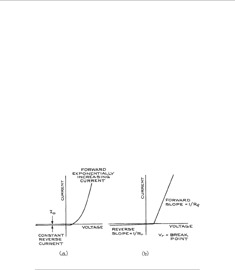
essentials, predict the behavior of complex circuits,
specify the operation of components , an d un derstand
and use data sheets and operation manuals. In routine
laboratory wor k, it is not necessary to be skillful with
circuit theory. It is necessary to be able to isolate the
basic elements of a circuit and understand their beh av-
ior. With that ability, when circuits fail to operate cor-
rectly, the causes of the malfunction can be localized
and repaired.
Linear circuit theory applies to devices whose output
is d irectly proportional to the applie d input. If o ne
increases the current through a resistor by a factor
of two, for example, the voltage across it will double.
An example of a nonlinear device is a switch that is
either open or closed and whose state changes abruptly
at a threshold. A n onlinear device can often be tr eated
with linear theory by dividing the response of the
device into separate regions over which it beh aves in a
quasi-linear manner. This is called linearizing the
response curve. An example is the piecewise lineariza-
tion of a d iode’s current–voltage response, as shown
in Fig ure 6.1. The exponentially rising forward current
and
constant reverse current are represented by straight
lines of slop e 1/R
f
and 1/R
r
, which are joine d at
voltage V
c
.
We begin by considering only passive linear devices;
that is, devices that either dissipate energy (resistors) or
store energy in electric (capacitors) or magnetic (inductors,
transformers) fields. Active devices, such as transistors, can
supply energy to a circuit when appropriately powered by
external sources. The analysis of circuits with active devi-
ces is based on representations using equivalent circuits
consisting of passive devices.
Con v entional circuit analysis uses three lumped circuit
elements – resistors (R), capacitors (C), and inductors (L).
This way of analyzing circuits is valid at signal frequencies f
for which the wav elength k is much larger than the physical
dimensions of the circuit. Since k ¼ c/f,wherec is the speed
of light, this means that analysis in terms of lumped elements
is valid up to frequencies of a few hundred megahertz.
This frequency limitation also excludes waveforms with
significant frequency components above a few hundred
megahertz, even though the repetition rate of the waveform
may be much less. A convenient way to estimate the fre-
quency of the highest-frequency component of a nonsinu-
soidal waveform is to divide 0.3 by the rise time of the
waveform, t
r
, defined as the time between the 10% and
90% amplitude points on the leading edge of the wave-
form. A pulse with a 10 ns rise time, for example, has
significant frequency components up to 30 MHz. The fall
Figure 6.1 (a) Real and (b) piecewise linear representation of the current–voltage
characteristics of a diode.
PRELIMINARIES 363
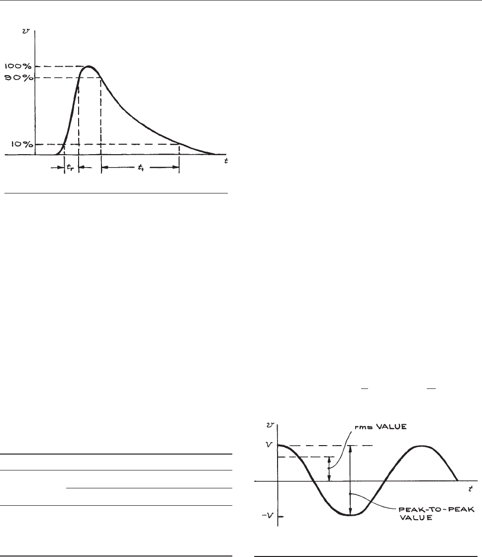
time, t
f
of a waveform is the time between the 10% and
90% amplitude points on the trailing edge. Figure 6.2
illustrates rise
time and fall time.
Even at low frequencies there are no ideal resistors, capaci-
tors, or inductors. Actual resistors have some capacitance and
inductance, while capacitors have resistance and inductance,
and inductors hav e resistance and capacitance. These depar-
tures from ideality are largely a matter of construction.
At high frequencies, stray capacitances and inductances
become significant, and one commonly speaks of distributed
parameters, in contrast to the lumped parameters at low fre-
quencies. Coaxial cable is an example of a type of distributed
parameter circuit. The electrical properties of coaxial cable
are normally given in terms of resistance and attenuation
per unit length as a function of frequency. At high frequen-
cies, the resistance of conductors (eve n connecting wires)
increases due to what is termed skin effect. The magnitude
of this effect for round cross-section wires is gi ven in Table
6.1 as a function of frequency. High-frequency connections
are
best made with leads having a large surface area-to-
volume ratio, with flat-ribbon geometry the best.
Conventional circuit theory is based on a few laws, prin-
ciples, and theorems. In the equations that follow, lowercase
letters represent instantaneous values of voltage and current,
whereas uppercase letters indicate effective or d.c. values. It
is also convenient to distinguish between root-mean-square
(rms), peak-to-peak, and average values of voltage and cur-
rent for sinusoidally varying voltages. If v ¼Vcos xt, where
v is the instantaneous value of voltage and V is the peak
value,thermsvalueisV=
ffiffiffi
2
p
, the peak-to-peak value is 2V,
and the average value is clearly zero. This is illustrated in
Figure 6.3. Common US line voltage is specified as 110 V
a.
c., which is the rms value. The peak voltage is 156 V, so
the peak-to-peak voltage is 312 V.
Under certain conditions, the rms value is not suffi cient
for specifying the output of an a.c. source. A source produc-
ing voltage spikes of large amplitude, but short duration
superimposed on a small sinusoidally varying voltage will
have an rms value very close to that without the spikes, but
the spikes can have a large effect on circuits connected to the
source. When specifying the output of a d.c. power supply,
the magnitude, frequency, and duration of nonsinusoidal
waveforms that appear at the output need to be specified,
as well as the rms value of any a.c. component of the output.
Laws
(i) Current–voltage relations. For resistors, capacitors,
and inductors we have:
v
R
¼ iR, v
C
¼
1
C
ð
idt, v
L
¼ L
di
dt
ð6:1Þ
Figure 6.2 Rise time (t
r
) and fall time (t
f
) of a pulse.
Table 6.1 Ratio of a.c to d.c wire resistance
Wire Gauge R
ac
/R
dc
10
6
Hz 10
7
Hz 10
8
Hz 10
9
Hz
#22 6.9 21.7 69 217
#18 10.9 34.5 109 345
#14 17.6 55.7 176 557
#10 27.6 87.3 276 873
Figure 6.3 Relation of rms and peak-to-peak voltages for a
sinusoidal waveform.
364 ELECTRONICS

respectively, where the resistance R is in ohms; the capaci-
tace C in farads; and the inductance L in henrys.
(ii) Loops and nodes (Kirchhoff’s laws). In these, the
sums are algebraic (signs taken into account):
(1) R (voltage drops around a closed loop) ¼ R (voltage
sources).
(2) R (current into a node) ¼ R (current out of a node),
where a node is a point where two or more elements
have a common connection.
Theorems
(i) Thevenin’s theorem. A real voltage source in a circuit
can always be replaced by an ideal voltage source in series
with a generalized resistance. An ideal voltage source is
one that can maintain a constant voltage across its termi-
nals regardless of the load across it. In other words, an
ideal voltage source has zero internal resistance. An auto-
mobile battery, with an internal resistance of a few hun-
dredths of an ohm, is a good approximation to an ideal
voltage source at currents of a few amperes. Electronically
regulated power supplies often have very low effective
internal resistances when operated within their voltage
and current ratings.
(ii) Norton’s theorem. A real current source in a circuit
can always be replaced by an ideal current source shunted
by a generalized resistance. An ideal current source is one
that supplies a constant current regardless of load – such a
source has an infinite internal resistance. Photo-multiplier
and electron-multiplier devices provide currents, albeit
very low, that are almost independent of load, and they
approximate ideal current sources.
Superposition, Circuits with Multiple
Sources
For a circuit that contains several sources (voltage, current,
or a combination of both) the contribution of each source
to the voltage between any two points or the current past a
point can be considered separately with all the other sour-
ces represented by their internal resistances. The total volt-
age or total current is then the algebraic sum of the separate
contributions of each of the individual sources.
When connecting a source of current or voltage to a
circuit, it is often important to know the internal resistance
of the source. This can be determined by first measuring the
open-circuit voltage of the source with a high internal-
resistance voltmeter and then connecting a variable
resistance across the source and adjusting it until the volt-
meter reading is one half the open-circuit value. The source
resistance is then equal to the value of the variable-resist-
ance setting. If the source has a very high internal resistance,
a current measurement can be substituted for the voltage
measurement. In this case, the output is shunted with an
ammeter and the so-called short-circuit current is measured.
Avariableresistanceisthenplacedinserieswiththe
ammeter and adjusted until the current through the ammeter
is one half the short-circuit current. The value of the variable
resistor at this point is equal to the internal resistance of the
source. Analogous measurements can be made for a.c. sour-
ces by using either a.c. voltmeters and ammeters or an
oscilloscope.
6.1.2 Circuit Analysis
For any given source, the choice of representation (Thevenin
or Norton) is arbitrary and, in fact, the series resistance in the
Thev enin representation is exactly equal to the parallel
resistance in the Norton representation. Thev enin’s and
Norton’s theorems simplify the application of the laws and
principles discussed above.
The most general method for solving circuit problems is
to apply Kirchhoff’s laws using the appropriate current–
voltage relations for each element in the circuit. This gives
rise to one or more linear differential equations, which,
when solved with the proper boundary conditions, give
the general solution. This is illustrated for RC circuits in
Section 6.1.3.
When
dealing with sinusoidal sources of angular fre-
quency x, circuit analysis can be greatly simplified when
only the steady-state solution is required. In this case, circuit
capacitances and inductances are replaced by r eactances:
capacitive reactance ¼ jX
C
, where X
C
¼
1
xC
inductive reactance ¼ jX
L
, where X
L
¼ xL
j ¼
ffiffiffiffiffiffiffi
1
p
ð6:2Þ
PRELIMINARIES 365
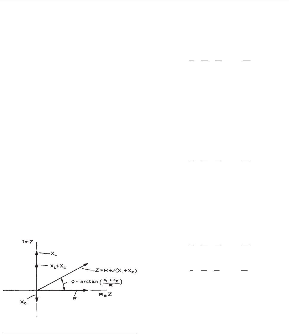
The impedance Z of a circuit is obtained by combining
reactances and resistances ac cording to the formula
Z ¼ R þ j(X
L
þ X
C
). These quantities can be represented
in the complex plane by vectors (see Figu re 6.4 ). The
angle
between Z and the real axis is /. By analogy with
the I–V relations for a pure resistance, X
C
is the ratio of
the a.c . voltage across a capacitor to the current t hrough
it, X
L
is the ratio of the a.c. voltage across an inductor to
the current through it, and Z is the net ratio of a.c. voltage
to current in a c ircuit composed of resistors, capacitors,
and inductors.
The fact that jX
C
and jX
L
are imaginary means that the
voltage and current are 90° out of phase with each other.
For a capacitor, the voltage lags the current by 90°, while
for an inductor the voltage leads the current by 90°.
Another quantity that is occasionally useful in circuit
analysis is the complex admittance Y, which is the recip-
rocal of the impedance. The SI unit of admittance is the
siemen. The usefulness of the admittance arises in circuits
with several parallel branches, where the net admittance is
the sum of the admittances of the branches.
In carrying out circuit analysis, the following results of
the above laws are useful:
Series Circuits. At any instant the current is the same
everywhere in a series circuit, and the algebraic sum of
the voltage drops around a circuit equals the algebraic
sum of the sources. For circuit elements of impedance
Z
1
, Z
2
, ..., Z
N
in an N element series circuit, the total
impedance is Z ¼ Z
1
þ Z
2
þþZ
N
. If all the elements
are resistors, or inductors, or capacitors, the general
expression reduces, respectively, to:
R ¼ R
1
þ R
2
þþR
N
1
C
¼
1
C
1
þ
1
C
2
þþ
1
C
N
L ¼ L
1
þ L
2
þþL
N
ð6:3Þ
Parallel Circuits. For circuit elements in parallel, the
voltage drop across each branch is the same while the
current through each branch is inversely proportional to
the impedance of the branch. The total current through
all of the branches is the voltage across the network
divided by the equivalent impedance for the network.
The equivalent impedance Z and admittance Y for an N
branch parallel circuit are:
1
Z
¼
1
Z
1
þ
1
Z
2
þþ
1
Z
N
ð6:4Þ
and:
Y ¼ Y
1
þ Y
2
þþY
N
ð6:5Þ
where Z
1
, Z
2
, ..., Z
N
are the impedances of the branches
and Y
1
, Y
2
, ..., Y
N
are the admittances . In t he special cases
where all the c ircuit elements in the branches are of the
same type:
1
R
¼
1
R
1
þ
1
R
2
þþ
1
R
N
C ¼ C
1
þ C
2
þþC
N
1
L
¼
1
L
1
þ
1
L
2
þþ
1
L
N
ð6:6Þ
where R, C, and L are the net resistance, capacitance, and
inductance of the circuits.
Voltage Dividers. The voltage divider, illustrated in
Figure 6.5(a), is a very common circuit element. The
instantaneous
voltage across Z
N
is v
in
[Z
N
/(Z
1
þZ
2
þ
Z
3
þþZ
N
)]; that is, the fraction of v
in
that appears
Figure 6.4 Relations between reactance, resistance,
impedance, and phase angle.
366 ELECTRONICS
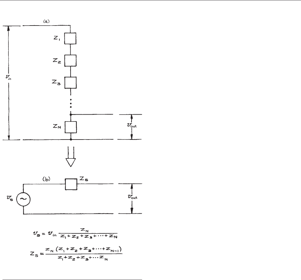
across any circuit element is the impedance o f that ele-
ment divided by the total impedance of the series circuit.
Voltage dividers provide a convenient way to obtain a
variable-voltage output from a fixed-voltage input, but
there are l imitations. To avoid drawing too much current
from the voltage source, the impedance of the voltage
divider string should not be too small. If, in the interest of
conserving power, however, the impedance is made
large, the output impedance of the circuit will be large
and v
out
will depend critically on the load. This can be
seen f rom the Thevenin equivalent of the circuit given in
Figure 6.5(b) wh ere v
s
is the instantaneous voltage of the
ideal voltage source. When Z
s
is large, the voltage across
a load will depend critically on the value of the load.
Such loading of a divider is to be avoided. For noncritical
applications, Z
s
should be at mo st 1/10 of any anticip ated
load.
Precision, highly linear, multiturn potentiometers are
commonly used for position sensing. In this application,
the shaft of the potentiometer is coupled mechanically
to the moveable element whose position is to be
determined, and a stable voltage source is connected
across the ends of the potentiometer. The ratio of the
voltage from the variable contact of the potentiometer
to its e nd gives the angle through which the shaft has
rotated.
Equivalent Circuits. Two circuits are equivalent if
the relationships between the measurable currents and
voltages are identical. As has been seen, a circuit with
two external terminals can b e replaced by its Thevenin or
Norton equivalent. Common equivalence transformations
for circuit s with three terminals (Mill er and Y–D trans-
formations) are shown in Figures 6.6 and 6.7.Inthefirst
Mi
ller transformation of Figure 6.6, it is necessary to
kno
w t he ratio of the voltages at nodes 1 and 2; in the
second it is necessary to know the ratio of the currents
into nodes 1 and 2.
Discussions o f amplifier circuits often refer to the
Miller effect. This occurs when the input and output
circuits of the amplifier are coupled by an impedance
Z#. By using the transformation in Figure 6.6,Z# bet
ween
input terminal 1 and output terminal 2 can be transformed
into an equivalent circuit where Z# is replaced by Z
1
and
Z
2
from terminals 1 and 2 to ground. The relations between
Z
1
,Z
2
, and Z# are given in the figure. When the coupling
between terminals 1 and 2 is capacitive with Z# ¼ 1/jxC#,
Z
1
and Z
2
are also capacitive impedances equal to
1/jxC#(1 K) and 1/jxC#K/(K 1), where K is the voltage
gain of the amplifier, negative for the example shown in
Figure. 6.6.
Figure 6.5 (a) The voltage divider; (b) the Thevenin
equivalent.
PRELIMINARIES 367
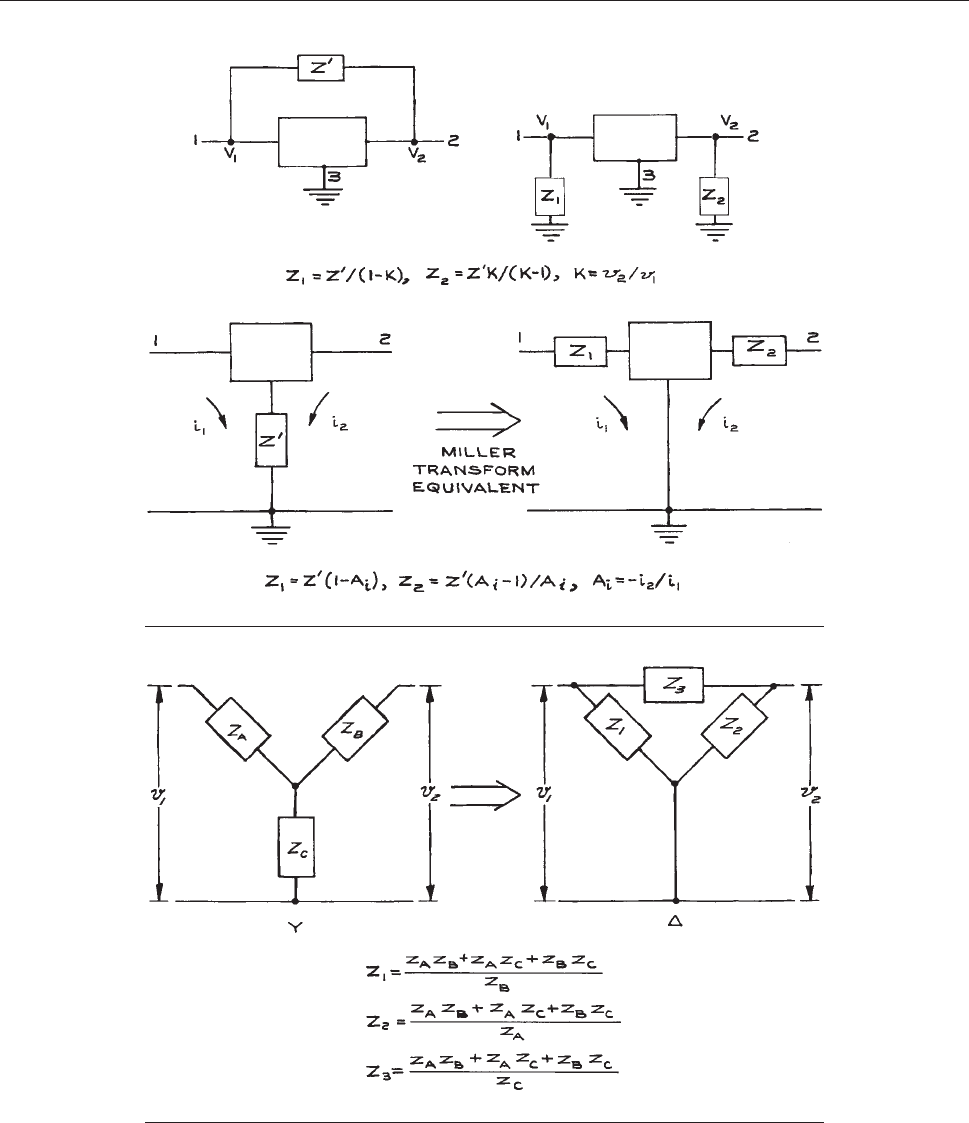
Figure 6.6 Miller transformations for circuits with three terminals.
Figure 6.7 Y–D transformation for a circuit with three terminals.
368 ELECTRONICS
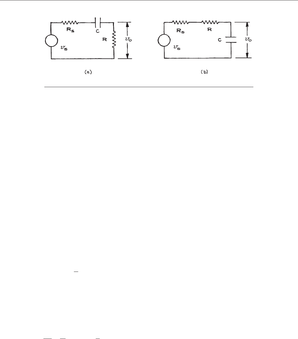
The Y–D transformation allows one to transform a cir-
cuit of three elements from a node to a loop configuration.
6.1.3 High-Pass and Low-Pass Circuits
Analysis of the high-pass and low-pass circuits shown in
Figure 6.8 illustrates some of the above circuit-analysis
principles.
The combination of v
s
and R
s
represents a real
voltage source with instan taneous open-circuit voltage v
s
and internal resistance R
s
. For the high-pass or differentiat-
ing circuit, the output voltage v
o
is across the resistor R;
for the low-pass or integrating circuit, it is across
the capacitor C. Very often, the essential properties of
complex circuits can be understood in terms of one of
these two circuits, so it is useful to be acquainted with
their characteristics.
These circuits can be analyzed by the differential-
equation method. For either circuit:
v
s
ðtÞ¼iR
s
þ
1
C
ð
idt þiR ð6:7Þ
This equation uses the fact that the sum of the voltage drops
in the circuit equals the sum of the voltage sources and the
current is the same everywhere in a series circuit at any
instant. Differentiating with respect to time:
dv
s
dt
¼
di
dt
ðR
s
þ RÞþ
i
C
ð6:8Þ
The solution to the homogeneous equation (dv
s
/dt ¼ 0) is:
i ¼ Ae
t=R#C
ð6:9Þ
where R# ¼ R
s
þ R and A is the integration constant
determined from the initial conditions. The general
solution requires that the functional form of v
s
be
known. Consider three cas es:
(1) An a.c. voltage of amplitude V:
v
s
¼ V cosðxt þ /Þð6:10Þ
(2) A step voltage of amplitude V:
v
s
¼
0 for t <0
V for t >0
ð6:11Þ
(3) A rectangular pulse of amplitude V and duration T:
v
s
¼
V for 0 < t < T
V for t <0,t > T
ð6:12Þ
For case 1, the output voltage is sinusoidal at the same
frequency as the input voltage. The ratio of v
o
to v
s
as a
function of normalized frequency is shown in Figure 6.9(a).
At
the frequencies x ¼x
H
and x ¼ x
L
for the two circuits,
v
o
is 1=
ffiffiffi
2
p
of the maximum value. These frequencies are
called the upper and lower corner frequencies, respectively.
The maximum power that can be delivered to a load is
proportional to the square of the output voltage, so that at
x ¼ x
H
and x ¼ x
L
, the maximum power that the circuits
Figure 6.8 (a) High-pass or differentiating circuit; (b) low-pass or integrating circuit.
PRELIMINARIES 369
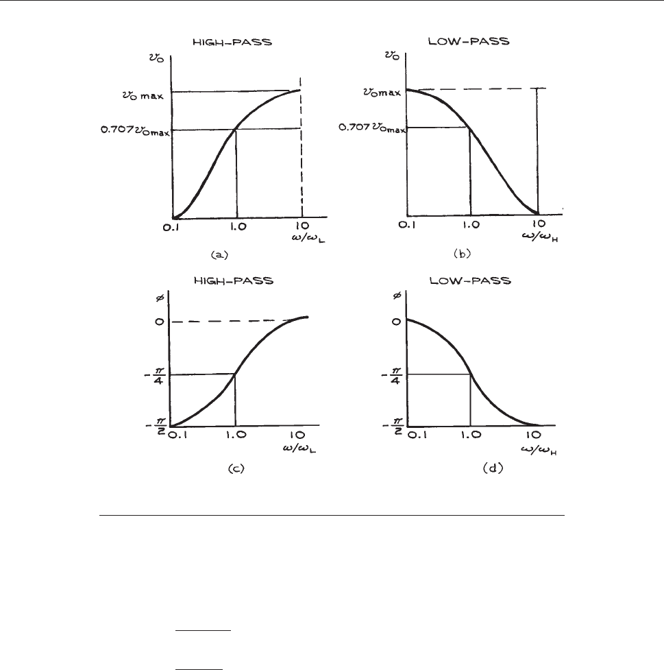
can deliver to a constant load is one-half the maximum
possible value. The usual way of expressing this is in terms
of decibels dB, where:
ratio in dB ¼ 10 log
10
power out
power in
¼ 10 log
10
v
2
out
=R
out
v
2
in
=R
in
ð6:13Þ
If R
out
¼R
in
, which is often assumed, then (ratio in dB) ¼
20 log
10
[v
out
/v
in
]. When m
out
=m
in
¼
ffiffiffiffiffiffiffiffi
1=2
p
, this is a pprox -
imately 3, so that 3 dB represents a power reduction
of a factor of two. Since the frequency response of ampli-
fiers,filters,andtransducersisroutinelygivenindB,itis
important to keep in mind that the dB scale is logarith-
mic. Human sensory per ception is approximately loga-
rithmic, and a 3 dB change in sound level or light level is
barely perceptible.
Because of the reactive element in the RC circuits (the
capacitor), the voltage is not in phase with the current, as
illustrated in Figure 6.9(b). These plots of phase and log
(output
voltage) as a function of log(frequency) are called
Bode plots, after H. W. Bode.
1
It is often convenient to approximate frequency-
response curves by a piecewise linear function. Such ideal-
ized Bode plots are shown in Figure 6.10(a) and (b). The
corner
frequencies are where x/x
L
and x/x
H
¼ 1.0.
Figure 6.9 Output voltage as a function of frequency for: (a) high-pass and (b) low-pass
circuits; phase as a function of frequency for: (c) high-pass and (d) low-pass circuits.
370 ELECTRONICS
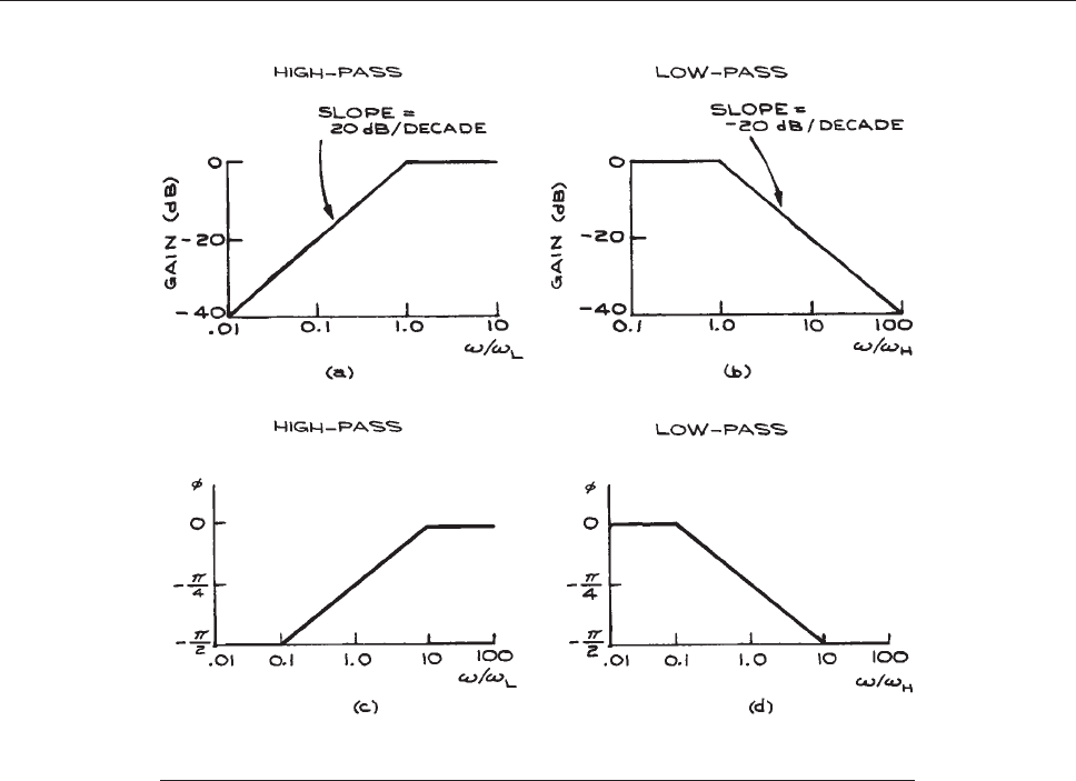
They correspond to the 3 dB points on the unapproxi-
mated Bode plots. For most purposes, the simplified curves
are satisfactory representations. From these curves, every
10-fold reduction in frequency below x
L
for the high-pass
circuit decreases the output voltage by 20 dB, and every
twofold reduction decreases it by 6 dB. The low-pass cir-
cuit has just the opposite properties: a 10-fold increase in
frequency above x
H
results in a 20 dB decrease in output
voltage, and a twofold increase results in a 6 dB decrease.
One often states these facts as 20 dB per decade and 6dB
per octave. The linearized phase-response curves are
shown in Figure 6.10(c). The 3
dB frequencies occur at
a phase shift of p/4 (45°) for the two circuits.
For the nonrepetitive input voltage waveforms of cases (2)
and (3), the output waveforms are given in Figure 6.11.
Th
e output, waveforms for the rectan gular-wave
input function can be used to determine the RC time
constants for differentiating and integrating circuits.
This is called square-wave testing. Th e RC time con-
stant for the differentiating circuit is obtained by using a
square-wave input with a rise time much smaller than
RC and a period much larger than RC. For times small
compared with RC, the tilt of the top edge of the output,
as viewed with a fast-rise-time oscilloscope (see Figure
6.
12) is directly related to RC.
The fractional decrease in
v
o
,intimet
1
is t
1
/RC, which can be set equal to (V V#)/V
and solved for RC. For the integrating circuit, RC is
obtained by measuring the rise time of the output waveform
on a fast-rise-time oscilloscope. Using the definition of
the rise time t
r
, as the time between the 10% and 90% points
Figure 6.10 Idealized gain response for (a) high-pass and (b) low-pass circuits; idealized
phase response for (c) high-pass and (d) low-pass circuits
PRELIMINARIES 371
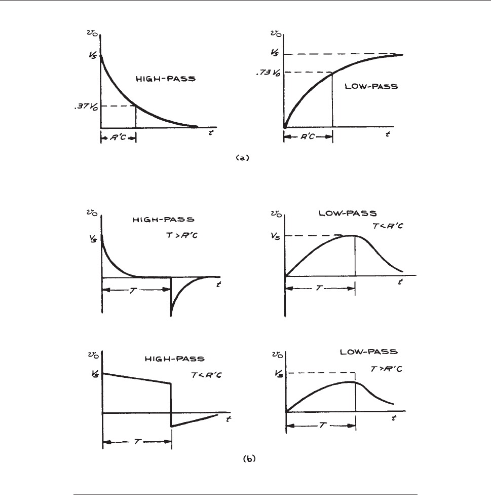
on the leading edge of the output waveform, one has the
relation:
t
r
¼ 2:2 RC ð6:14Þ
6.1.4 Resonant Circuits
The voltages and currents in circuits with capacitors, induc-
tors, and resistors show oscillatory properties much like
those of mechanical oscillators. Electronic circuits ha v e
Figure 6.11 Response of high-pass and low-pass circuits to a step voltage (a) and a
rectangular pulse of duration T (b).
372 ELECTRONICS
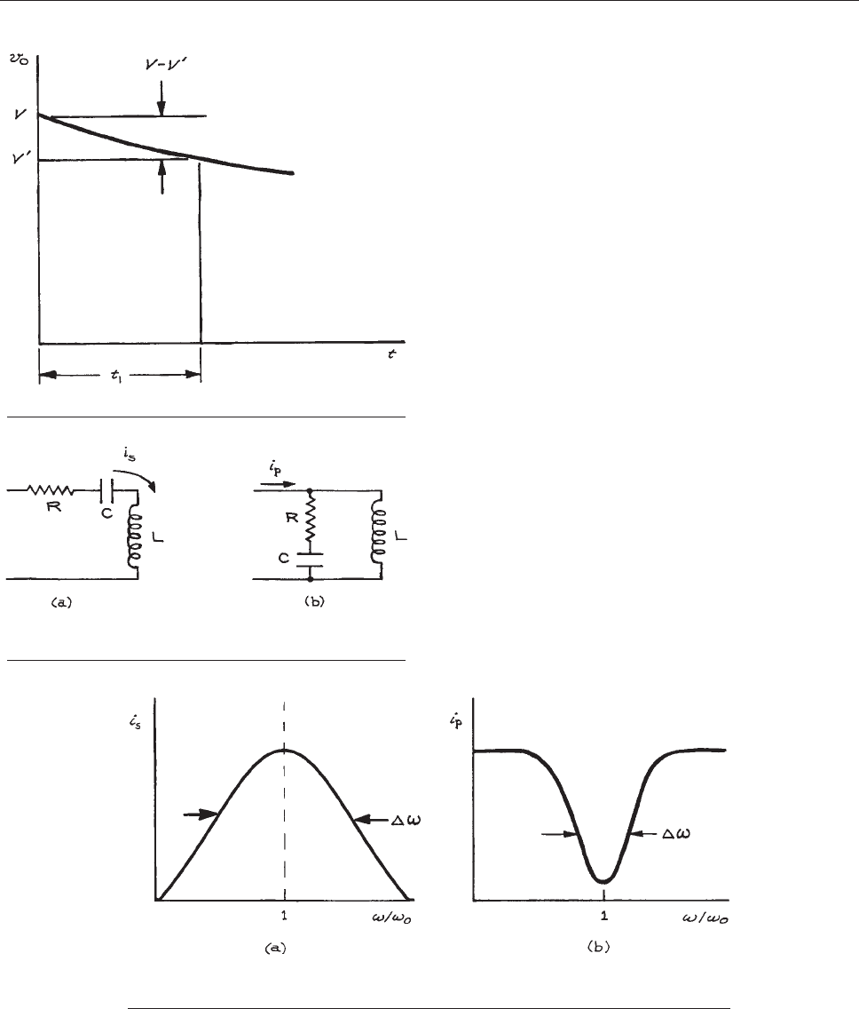
natural frequencies of oscillation and can be critically
damped, underdamped, or overdamped, depending on
the relations between the values of the circuit parameters.
Resonant circuits with ideal capacitors and inductors are of
the series or parallel type sho wn in Figure 6.13.Whendriven
b
y a sinusoidal input source, the capacitativ e reactance in the
series circuit will cancel the inducti v e reactance at the
resonant frequenc y x
o
, where 1/Cx
o
¼ x
o
L and
x
o
¼
ffiffiffiffiffiffiffiffiffiffiffi
1=LC
p
.Atx
o
the impedance of the series circuit is
a minimum and the current through it is a maximum.
For the parallel resonant circuit at low frequencies, the
L branch will have a very low reactance and the current
drawn from the source will flow almost entirely through
that branch. At high frequencies, the current through the
RC branch is limited by the value of R. The total impe-
dance of the parallel circuit is therefore small at low and
high frequencies, passing through a maximum at the fre-
quency x
o
¼
ffiffiffiffiffiffiffiffiffiffiffi
1=LC
p
, provided that R << x
o
L. Graphs of
the currents in the two circuits as a function of driving
frequency are given in Figure 6.14. Real inductors have
an
associated resistance, which generally must also be
taken into account when analyzing circuits.
One measure of the resonance sharpness in the series and
parallel circuits is the Q or quality of the circuit. For prac-
tical purposes, Q ¼ x
o
/Dx where Dx is the full width at
half maximum of the peak or valley. In terms of the circuit
parameters, 1/Q ¼ x
o
L/R ¼ 1/x
o
RC. This is the ratio of the
energy stored (in the capacitor or inductor) to the energy
dissipated in the resistor per cycle at resonance. Values of Q
Figure 6.12 Square-wave testing of a high-pass circuit.
Figure 6.13 (a) Series resonant circuit; (b) parallel resonant
circuit.
Figure 6.14 Current as a function of frequency for: (a) the series resonant circuit and
(b) the parallel resonant circuit.
PRELIMINARIES 373
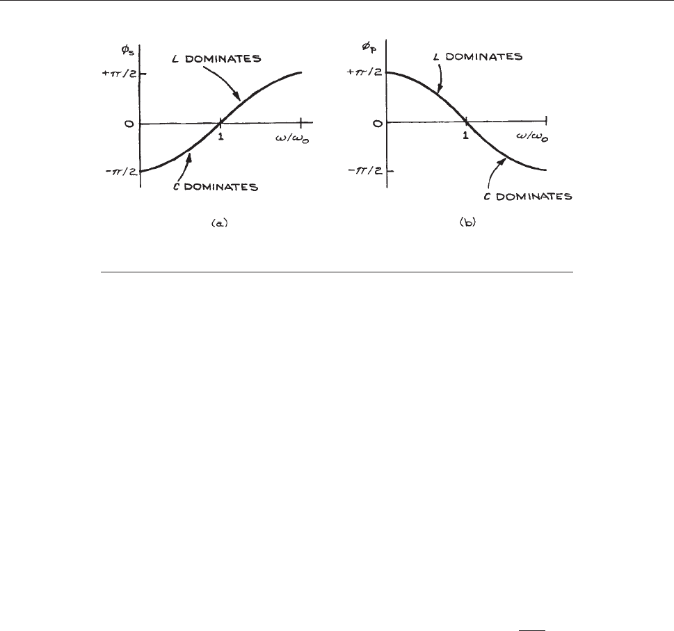
as large as 100 can be attained in electrical circuits while
mechanical oscillators can attain values as high as 10
6
. The
phase relationships between voltage and current in series
and parallel resonant circuits are shown in Figure 6.15.
T
hebehaviorofanLRC circuit upon the application of a
step or rectangular input is much like the response of a
mechanical system to a sudden impulse. Critically damped,
underdamped, and overdamped current flows result.
6.1.5 The Laplace-Transform Method
A general technique for analyzing circuits for arbitrary
input voltage waveforms is the method of Laplace
transforms. With this method it i s possible to use onl y
algebra and lists of transforms – such as t hose given in
Table 6.2 – for the s olution of differential equations and
the
evaluation of boundary c onditions. The results of the
method will be presented without any proofs. The
vocabulary of Laplace transforms occurs in the discus-
sion of circuits and is included in this chapter for that
reason.
The method is based on an integral transform of the type:
f ðs Þ¼
ð
‘
0
f ðtÞe
st
dt ð6:14Þ
where
f ðsÞ is the Laplace transform of f(t), written as
L [f(t)]. The function f(t) can involve integrals and dif-
ferentials. When L is applied to the second-order differ-
ential equations that arise in circuit analysis, rather
important simplifications occur a nd results can often be
written down by inspection. The Laplace transform of
the output voltage
v
o
ðsÞ of a circuit is the Laplace trans-
form of the input voltage
v
i
ðsÞ times the Laplace tra ns-
form of the transfer function
TðsÞ–thetransfer function
being the function relating the output to input. To obtain
TðsÞ, the values of all elements in the circuit are replaced
by their transform equivalents according to the recipe
R / R, C / 1/sC,andL / sL . In the simple case of
the voltage divider, the transfer function is t he ratio of the
impedance of the output-circuit element to the total
impedance of the circuit chain. T(s) is obtained in exactly
the same way, using the equivalences for R, C,andL.In
general,
TðsÞ is in the form of a ratio of two functions of
s, G(s)andH(s), which are polynomials in s:
TðsÞ¼
GðsÞ
HðsÞ
ð6:15Þ
The values of s for which G(s) is zero are called the zeros
of
TðsÞ; the values of s for which H(s) is zero are the
locations of the poles of
TðsÞ. In the most general case,
the zeros and poles are complex. The positions of the zeros
and poles of
TðsÞ in the complex plane give important
information on the properties of the circuit under analysis.
When the poles are complex, they occur in pairs, while
Figure 6.15 Phase relations between voltage and current in: (a) the series resonant
circuit and (b) the parallel resonant circuit.
374 ELECTRONICS

Table 6.2 Elementary Laplace Transforms
f(t)(t >0)
f ðsÞ
d(t)1
11/s
t
n1
/(n 1)! 1/s
n
(n a positive integer)
e
at
1
s a
sin at
a
s
2
þ a
2
cos at
s
s
2
þ a
2
sinh at
s
s
2
a
2
cosh at
s
s
2
a
2
t
2a
sin at
s
ðs
2
þ a
2
Þ
2
1
2a
3
ðsin at at cos atÞ
1
ðs
2
þ a
2
Þ
2
df ðt Þ
dt
s
f ðsÞf
0
, f
0
¼ lim
t!0
f ðt Þ
d
2
f ðt Þ
dt
s
2
f ðsÞsf
0
f
1
, f
1
¼ lim
t!0
df ðt Þ
dt
R
t
0
f ðt
0
Þdt
0
1
s
f ðsÞ
1
a b
ðe
at
e
bt
Þ
1
ðs aÞðs bÞ
1
a b
ðae
at
be
bt
Þ
s
ðs aÞðs bÞ
1
a
2
ð1 cos atÞ
1
sðs
2
þ a
2
Þ
1
a
3
ðat sin atÞ
1
s
2
ðs
2
þ a
2
Þ
1
abðb
2
a
2
Þ
ðb sin at a sin btÞ
1
ðs
2
þ a
2
Þðs
2
þ b
2
Þ
1
b
2
a
2
ðcos at cos btÞ
s
ðs
2
þ a
2
Þðs
2
þ b
2
Þ
1
a
2
þ b
2
e
at
b
ffiffiffiffiffiffiffiffiffiffiffiffiffiffiffi
a
2
þ b
2
p
sin½bt þ argð a þ ibÞ
1
s ðs þ aÞ
2
þ b
2
hi
PRELIMINARIES 375
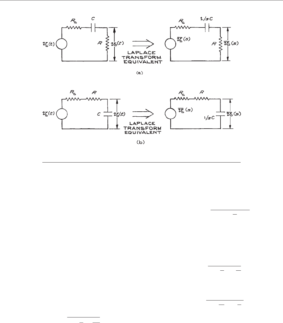
real-valued poles can occur singly or in pairs. The values of
the real and imaginary components of the pole coordinates,
usually labeled r and x, have important physical meaning.
The real component r is a measure of the damping in the
circuit while the imaginary part x is the natural frequency
of oscillation. Negative values of r give stable circuits in
which transient signals all decay to zero with time. Circuits
employing only passive elements behave in this way and
are stable. Circuits with active elements can behave in such
a way that the output increases with time in response to a
transient input signal. Such circuits are unstable and have
values of r greater than zero. They are to be avoided,
except in the case of oscillators, which must be unstable
in order to function.
The Laplace-transform equivalents of the high-pass
and low-pass circuits are shown in Figure 6.16. For the
high-pass
circuit, the output voltage across the resistor R
for the transformed circuit is:
v
o
ðsÞ¼
v
s
ðsÞ
1
ð1 þ
R
s
R
Þþ
1
SRC
ð6:16Þ
where
TðsÞ, the transfer function, has a pole at s ¼1/(R
+ R
s
)C. For the low-pass circuit, the ou tput voltage across
the capacitor for the transformed circuit is:
v
o
ðsÞ¼
v
s
ðsÞ
1
1 þð1 þ
R
s
R
ÞSRC
ð6:17Þ
TðsÞ has a pole at S ¼1=ðR þ R
s
ÞC. The steady-state
frequency and phase response of the circuits are obtained
from
TðsÞ by replacing s with jx. The transfer functions
are now, for the high-pass circuit:
TðxÞ¼
1
ð1 þ
R
s
R
Þj
x
L
x
ð6:18Þ
and:
TðxÞ¼
1
1 þ j
x
x
H
ð1 þ
R
s
R
Þ
ð6:19Þ
for the low-pass circuit. For these circuits x
L
¼ x
H
¼ 1/RC
for R
s
jR<<j.
Figure 6.16 Laplace-transform equivalents of: (a) the high-pass and (b) the low-pass
circuit.
376 ELECTRONICS
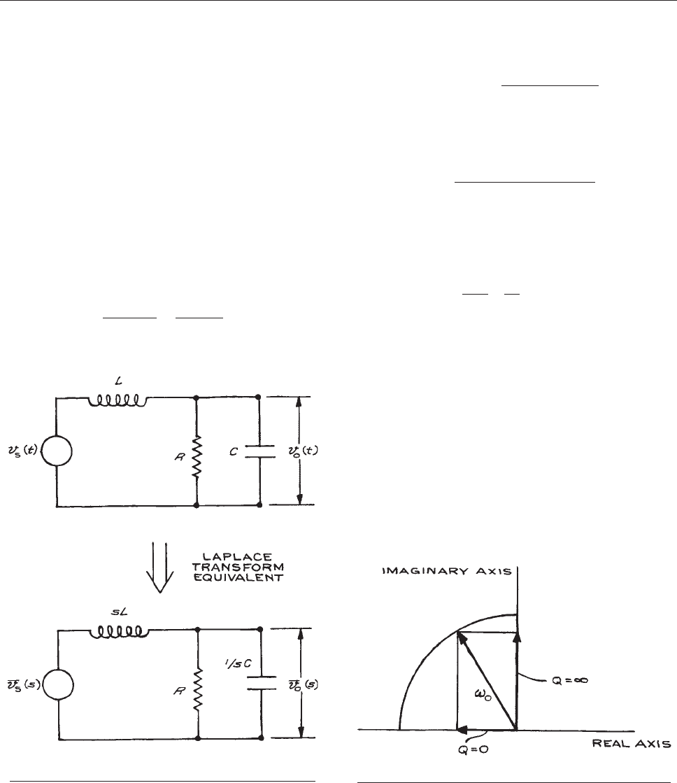
As seen previously, x
L
and x
H
are the corner
frequencies of the circuits. By rationalizing the denomina-
tors of the transfer functions, one obtains the phase
response. Since there are no inductive elements in the cir-
cuits, there is no natural frequency of oscillation. The poles
lie on the negative real axis because there are no active
elements in the circuit to cause sustained oscillations.
6.1.6 RLC Circuits
Consider the equivalent circuit and the Laplace transform
given in Figure 6.17. To analyze the circuit, consider the
parallel
combination of R and 1/sC, which is in series with
sL in a voltage-divider configuration:
R=sC
R þ 1=sC
¼
R
1 þ sRC
ð6:20Þ
Thus:
v
o
ðsÞ¼
v
i
ðsÞ
1
1 þ sL=R þ s
2
LC
ð6:21Þ
The poles of
TðsÞ occur at:
s ¼
L=R6
ffiffiffiffiffiffiffiffiffiffiffiffiffiffiffiffiffiffiffiffiffiffiffiffiffiffiffiffi
ðL=RÞ
2
4LC
q
2LC
ð6:22Þ
Letting the natural frequency of oscillation of the circuit be
x
0
¼ 1=
ffiffiffiffiffiffi
LC
p
,wehaveQ ¼ R/x
0
L
0
, and the poles can be
rewritten as:
s ¼
x
0
2Q
6
x
0
2
ffiffiffiffiffiffiffiffiffiffiffiffiffiffiffiffiffiffiffi
1=Q
2
4
q
ð6:23Þ
There are three different possibilities for the roots of s:
(1) 1/Q
2
¼ 4: a single real root at s ¼x
0
/2Q
(2) 1/Q
2
4 ¼ m
2
(m real): two real roots at s ¼x
0
/2Q
6 x
0
m/2.
(3) I/Q
2
4 ¼m
2
(m real): two conjugate complex roots
at s ¼x
0
/2Q 6 jx
0
m/2.
The magnitude of s in the r, jx plane is x
0
; in geometric
terms this means that the roots of s are confined to a semi-
circle of radius x
0
in the left half of the complex plane (see
Figure 6.18).
Figure 6.17 An RLC circuit and the Laplace-transform
equivalent.
Figure 6.18 Pole trajectory for an RLC circuit.
PRELIMINARIES 377
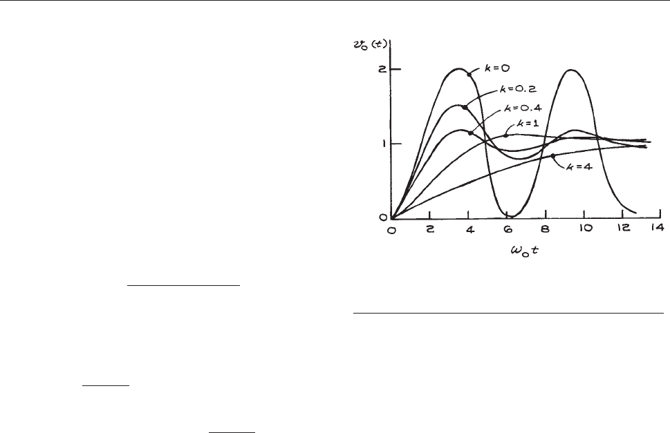
6.1.7 Transient Response of
Resonant Circuits
The stability of a linear system subjected to a driving func-
tion depends on the system itself rather than the driving
function. For ease of analysis, consider the RLC circuit of
Figure 6.17 to be driven by a unit step input voltage of the
fo
rm v
i
(t) ¼ 1 for t > 0. The Laplace transform of the output
voltage is then the transform of the input voltage,
v
i
ðsÞ,
multiplied by the transform of the transfer function
TðsÞ:
v
o
ðsÞ¼
v
i
ðsÞ
TðsÞð6:24Þ
For the unit step, input v
i
(s) ¼ 1/s from Table 6.2; therefo re
v
o
ðsÞ¼
1
sð1 þ sL=R þ s
2
LCÞ
ð6:25Þ
To find v
o
(t) it is necessary to look up the inverse transform
in Table 6.2. The result is:
v
o
ðtÞ¼1
e
kx
0
t
ffiffiffiffiffiffiffiffiffiffiffiffiffi
1 k
2
p
sin
"
ffiffiffiffiffiffiffiffiffiffiffiffiffi
1 k
2
p
x
0
t
þarctan
ffiffiffiffiffiffiffiffiffiffiffiffiffi
1 k
2
p
k
!#
ð6:26Þ
where k ¼ 1/2Q. Critical damping, overdamping, and
underdamping correspond to k ¼ 1, k > 1, and k <1,
respectively. The normalized response of the circuit for
various values of k is shown in Figure 6.19.
A
s can be seen, th e underdamped waveform overshoots
the steady-state value of one and oscillates about it with
decreasing amplitude. This is sometimes called ringing.
As damping is increased, the output waveform oscilla-
tions decrease in amplitude until, for k ¼1 (critical damp-
ing), the oscillations are completely gone. Increasing the
damping beyond k ¼ 1 only i ncreases the time for the
waveform to arrive at the steady-state value.
Overshoot, rise time, settling time, and error band are
terms used to characterize output waveforms. They are
illustrated in Figure 6.20. For critical damping, t
r
¼ 3.3/
x
0
. By decreasing the damping so that k <1,t
r
can be
further decreased, but at the expense of ringing. A suitable
compromise that is often used is k ¼ 0.707, under which
circumstance the overshoot is 4.3% and t
r
is reduced to
2.16/x
0
. Figure 6.21 is a graph of the percentage overshoot
as a function of k.
The abov e analysis is not restricted to passive circuits.
Amplifiers with negati v e feedback can have response
functions identical in form to those for RLC circuits. The
response of such amplifiers to nonrepetiti ve waveforms is
specified using the same terms as for the passi ve circuit
above. In pulse amplifiers, the transient response is the fun-
damental limitation on the pulse repetition rate. For critically
damped amplifiers, the width T of the impulse response and
the rise time t
r
are approximately related by T ¼ 1.5t
r
,sothat
pulsescannotbesentatarategreaterthan1/T per second. T,
in this case, is generally taken to be the time between the 50%
points on rising and falling edges of the output waveform.
For the precision control of temperature in a thermostat,
three-term control is often used. With this method, the
power applied to the heater element is set equal to a constant
background level plus a term proportional to the difference
between the set-point temperature T
s
and current temper-
ature T, a term proportional to the time integral of T
s
T,
and a term proportional to the time derivative of T
s
T.The
resulting differential equation is, under certain circumstan-
ces, analogous to that for the RLC circuit. Experimental
parameters are chosen to obtain the fastest time response
consistent with overall system stability. This is discussed in
further detail in Section 6.7.9 and in Chapter 7.
Figure 6.19 Response of a resonant circuit with no
damping (k=0), underdamping (k=0.2, 0.4), critical
damping (k=1), and overdamping (k=4).
378 ELECTRONICS
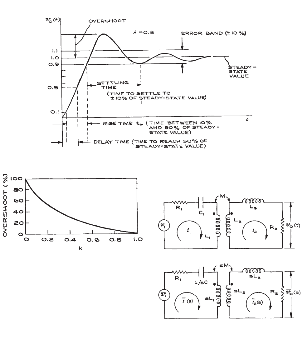
6.1.8 Transformers and Mutual Inductance
Transformers consist of primary and secondary windings
coupled by a core, which can be of magnetic material or
air. A voltage is induced in the secondary of the trans-
former when there is a change of current in the primary.
The reverse also occurs – indu ced volt age in the primary
due to a current change in the secondary. A transformer
circuit and the Laplace-transform equivalent are illus-
trated in Figure 6.22. T he dot associated with each
Figure 6.20 Output waveform in an underdamped resonant circuit.
Figure 6.21 Percentage overshoot as a function of
damping in a resonant circuit.
Figure 6.22 A transformer circuit and the
Laplace-transform equivalent. M, the mutual inductance,
is positive if i
1
and i
2
both flow into or out of the dotted
ends of the coils.
PRELIMINARIES 379
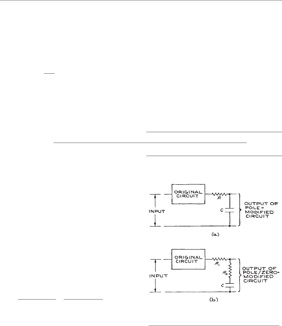
winding of the transformer indicates the relative orienta-
tion of the windi ngs. The convention is that M,themutual
inductance, is positive if the currents i
1
and i
2
both flow
into or out of the dotted ends of the coils, and negative
otherwise. The transfe r function
TðsÞ is obtained by
applying Kirchhoff’s laws to the two loops:
v
i
ðsÞ¼R
1
i
1
ðsÞþ
i
1
ðsÞ
sC
þ
i
1
ðsÞsL
1
sM
i
2
ðsÞ
0 ¼
i
2
ðsÞsL
2
i
1
ðsÞsM þ
i
2
ðsÞsL
3
þ
i
2
ðsÞR
2
ð6:27Þ
v
o
ðsÞ¼
i
2
ðsÞR
2
Eliminating
i
1
ðsÞ and substituting for
i
2
ðsÞ in the third
equation gives the result:
6.1.9 Compensation
It is often desired to modify the frequency response of a
given circuit. Two common methods are the addition of a
pole that is much smaller than the other poles of the trans-
fer function and the simultaneous addition of a pole and
zero to the transfer function. The addition of a pole is
accomplished with a resistor and capacitor in a low-pass
configuration at the output of the circuit to be modified, as
illustrated in Figure 6.23(a). If the original circuit had a
pole x
1
and the introduction of the RC circuit produced a
pole at x
2
where x
2
<< x
1
, the overall response of the
circuit would be a 20 dB/decade decrease in gain from x
2
to x
1
followed by a 40 dB/decade decrease for frequencies
greater than x
1
.
The addition of a pole and a zero is accomplished with
the circuit in Figure 6.23(b). The transfer function for the
pole-zer
o compensation network is:
R
2
þ 1=sC
R
1
þ R
2
þ 1=sC
¼
1 þ sR
2
C
1 þ sðR
1
þ R
2
ÞC
ð6:29Þ
with the zero at s ¼1/R
2
C and the pole at s ¼1/(R
1
þ
R
2
)C. If the zero in the transfer function is chosen to
cancel the smallest pole of the original circuit, the overall
frequency response will be flat up to the frequency
corresponding to the new pole. The gain will then decrease
by 20 dB/decade with increasing frequency up to the sec-
ond pole of the original circuit. The gain will then decrease
by 40 dB/decade up to the next high-frequency pole, after
which the decrease will be 60 dB/decade. The response of
the pole-zero-compensated circuit is sharper than that of
one with single-pole compensation.
6.1.10 Filters
Filters are generally classed as low-pass, high-pass, band-
pass, and band-reject. RC circuits are examples of the first
two kinds, while the series and parallel RLC circuits illus-
trate the last two. A series of band-pass or band-reject
filters with pass bands at different, but closely spaced,
frequencies is called a comb filter.
Figure 6.23 Compensation by: (a) the addition of a pole
and (b) the addition of a pole and a zero to cancel the
lowest-frequency pole of the original circuit.
v
o
ðsÞ¼
v
i
ðsÞ
R
2
MCs
2
CL
1
ðL
2
þ L
3
ÞM
2
s
3
þ R
1
ðL
1
þ L
2
ÞþR
2
L
1
½Cs
2
þ L
2
þ L
3
þ R
1
R
2
C½R
2
s þ R
2
ð6:28Þ
380 ELECTRONICS

The ideal filter would pass unattenuated all frequencies
in its pass band while completely rejecting frequencies
outside the pass band. The simple circuits we have exam-
ined thus far are only approximations to the ideal. There
are excellent approximations to the ideal filter that rely on
judicious choices of the transfer function poles of RC and
RLC circuits. There are four classes of filter design, each of
which has its advantages:
(1) Maximally flat has the flattest amplitude response within
the pass band. The Butterworth filter is an example.
(2) Equal ripple has fluctuations in the pass band but
greater attenuation in the stop band than the maxi-
mally flat filter.
(3) Elliptic has the maximum rate of attenuation between
the pass band and stop band. The Chebyshev filter is an
example of this type.
(4) Linear phase has a much less sharp cutof f than the others,
but maintains an almost linear phase response in the
pass band. The Bessel filter is an example of this type.
Methods of filter design are well established, and there
are many texts and handbooks that provide tables for filter
synthesis. Before designing or specifying a filter, it is
important to know, not only the cutoff and phase proper-
ties, but also the transient response and the input and out-
put impedances.
Amplifiers with negative feedback provided by resis-
tors and capacitors ca n have responses identical to RLC
circuits. By appropriate choices of the elements in a
feedback network, these amplifiers can be made into
filters. These so-called active filters are especially useful
at low frequencies, where large inductors with low resist-
ance are heavy a nd expensive. There are m any texts
and handbooks on active-filter design. Lancaster’s Active
Filter Cookbook (D. Lancaster, 2nd ed., Butt erworth-
Heinemann, Oxford, 1996) is written from a practical
point of view with a minimum of mathematics. Most
active-filter designs are based o n high-gain integrated-
circuit operationa l amplifiers. With the frequency
response of these amplifiers now extending well into
the megahertz region, active filters are finding increasing
application to high-frequency circuits. Stability is an
important factor in filter design, especially for large
values of Q. If drift is to be minimized, highl y stable
passive components are required.
6.1.11 Computer-Aided Circuit Analysis
The Simulation Program with Integrated-Circuit Emphasis
(SPICE) was originally intended for integrated circuit
design where the very large number of circuit elements
made traditional circuit analysis slow, cumbersome, and
subject to errors. The SPICE Program was first limited to
use on mainframe computers with network access, but var-
ious versions are now available for personal computers
(PCs). One popular PC version of SPICE is PSPICE, now
available from Cadence. Because SPICE and PSPICE fig-
ure prominently in electrical-engineering circuit-analysis
courses, they are usually available over university networks
and various versions, including student/faculty and evalua-
tion versions, can be downloaded from the web. Analysis of
digital circuits with SPICE requires detailed information
about waveforms and delays within individual units. Dig-
ital circuits are increasingly assembled from programmable
arrays and the manufacturers of the arrays generally supply
the required information with their programming software.
The following procedures should be followed when
using circuit-analysis programs:
(1) Create a schematic diagram of the circuit:
Assemble components from the program library
Import or create components unavailable in library
Assign values to resistors, capacitors, and
inductors
Make interconnections
(2) Create SPICE/PSPICE file:
Specify temperature
Specify sources
– Independent
– Controlled
Verify interconnections (nodes)
(3) Analysis:
D.c., quiescent
Transient
A.c., small signal
(4) Output:
Graphs
– Bode plots
– Waveforms
– Numerical tables
(5) Adjust circuit to meet design criteria and reanalyze.
PRELIMINARIES 381

Analysis programs are extremely useful, but cannot
replace an understanding of circuit theory. It is unrealistic
to believe that one can begin with an approximate circuit
and use a program to arrange the values of the components
and the configuration until the desired result is attained.
Even for a simple circuit of 10 components, the number of
possibilities is so large that an uninformed attempt to arrive
at a desired final result cannot be successful. On the other
hand, an arbitrary circuit can be analyzed to determine
whether it will perform according to the requirements.
Most analysis programs come with libraries of common
active devices (transistors, diodes, operational amplifiers)
however, new devices appear on the market daily and
older devices become obsolete so th at it is imprac tical
for any single library to contain all possible devices. Add-
ing device specifications to analys is prog ra m libraries ca n
be time consuming and it is often more e fficient to use
available devices with operating parameters close to those
of the device in question. This requires additional research,
but device specifications are now routinely available on the
websites of the manufacturers. In some cases, manufac-
turers provide SPICE files for their devices for loading
directly into libraries. An additional benefit of analysis pro-
grams is compatibility with schematic capture and printed-
circuit-board layout software. This is discussed in more
detail in Section 6.10.3 on printed circuit boards.
6.2 PASSIVE COMPONENTS
In discussing passive components, emphasis will be placed
on choosing the correct type for the function to be per-
formed. It is rarely sufficient to specify the nominal value
of a component. This can be appreciated by looking through
the catalog of any electronics supplier under resistors and
finding perhaps 50 different resistor types, each with a range
of resistance values. The following are some general con-
siderations in the choice of passive components:
(1) Nominal value and tolerance. An aspect of this is the
coding applied to the component. Color, letter, and
number codes are used.
(2) Stability. The nominal value as a function of temperature
[the temperature coefficient (tempco) is often expressed
in % or in parts per million change per °Corppm/°C].
Age and en vironmental conditions such as humidity,
vibration, or shock also effect component v alues. On the
other hand, components can affect their environment –
for example, the outgassing of a capacitor in vacuum or
the heating of one component by another.
(3) Size and shape. Along with the reduction in size that
solid-state electronics has brought, there has been a
similar reduction in the size of passive components.
Generally, one uses the smallest practical size, but
power -density considerations can limit the packing den-
sity of power-dissipating components. Also, components
come in different shapes with dif fer ent lead geometries
depending on the intended mounting method. These are
discussed in the section on hardware.
(4) Power dissipation and voltage rating. A resistor has both
a po wer rating and a voltage rating. For very large values
of resistance, it is quite possible to operate well within
the resistor’s power rating, yet exceed the voltage rating.
The result is electrical breakdo wn and destruction of the
resistor. For moderate values of capacitance, capacitors
dissipate very little power and power rating is of no
importance. Very-high-capacitance capacitors with large
effective surface areas, however, have non-negligible
shunt conductances. The large currents that flo w in such
capacitors can cause considerable heat to be generated
with potentially fatal (to the capacitor) results.
(5) Noise. Passive components can introduce noise into an
electronic circuit, and one must be particularly aware
of this problem in low-level circuits and choose appro-
priate low-noise components.
(6) Frequency characteristics. Pure resistors, capacitors,
and inductors are practically unrealizable, and the elec-
trical properties of real passive components depend on
frequency in a nonideal way. This is often indicated by
an equivalent circuit. Inductors and transformers with
magnetic cores, however, are inherently nonlinear and
can be treated only approximately in this way.
(7) Derating. This is an engineering term related to the
safety factors to be used when operating components
under a variety of conditions. Good design requires that
components be operated at no more than 50% of the
manufacturer’s recommended maximum ratings, partic-
ularly with respect to power and voltage. At high ambi-
ent temperatures, components should be derated by even
larger amounts. The resulting decrease in stress greatly
increases component lifetime. In laboratory equipment,
382 ELECTRONICS

large safety factors should always be used for enhanced
reliability. The abbreviation SOA, safe operating area,
specifies the limits of voltage, current, and temperature
for semiconductors.
(8) Cost. For laboratory applications it is poor practice to
economize on passi v e components by using the least e x-
pensiv e ones that will do the job. Laboratory work is labor
intensiv e. The extra cost of top-grade components greatly
outweighs the time saved in troubleshooting and repair .
6.2.1 Fixed Resistors and Capacitors
The more common types of fixed and variable resistors and
fixed capacitors are listed in Tables 6.3 to 6.5.InTable 6.5,
the C range
and V range refer to the minimum and max-
imum values available for all types of a given dielectric. It
is not possible to have the maximum capacitance at the
maximum voltage. The larger capacitances have lower
working voltages (WV), while the smaller ones have the
Table 6.3 Fixed resistors
Carbon Composition Precision Wire-Wound (bobbin)
R range: 2.7 X to 22 MX R range: 0.1 X to 18 MX
Power range:
1
10
to 2W
Power range:
1
10
to 2W
Tolerances: 6 5, 6 10, 6 20% Tolerances: 6 0.05 to 6 5%
Temperature range: 55 to + 150 °C Temperature range: 55 to 6 145 °C
Temperature coefficient 6 0.1%/°C Temperature coefficient 6 0.0001 to 6 0.002%/°C
Voltage coefficient 6 0.03%/V d.c. Noise: Low
Noise: Highest Frequency response: To 25 kHz for high-resistance values
unless noninductively wound
Typical capacitance: 0.25 pF, no inductance
Working voltage:
150V
1
8
W
to 750Vð2WÞ
Precision Carbon Film Power Wire-Wound
R range: 1 X to 100 MX R range: 0.1 X to 1.3 MX
Power range:
1
10
to 2W
Power range: 2 to 225 W
Tolerances: 6 0.5, 1, 2% Tolerances: 6 5%, 6 10%
Temperature range: 55 to 165 °C Operating temperature: 75 to +350 °C
Temperature coefficient 0.02 to 0.05%/ °C Maximum rated-power
temperature:
25 °C
Noise: Low Temperature coefficient: 6 0.026%/°C
Frequency response: To 1 MHz for R >1kX(spinal),
to 100 MHz for R <1kX
Frequency response: To 25 kHz for high-resistance values
unless noninductively wound
Precision Metal Film
R range: 10 X to 200 MX
Power range:
1
8
to
1
2
W
Tolerances: 6 0.1 to 6 1%
Temperature range: 55 to 165 °C
Temperature coefficient 0.0025 to 0.01%/°C
Noise: Lowest
PASSIVE COMPONENTS 383

higher WV. The temperature coefficients generally apply
only to a limited temperature range within the larger oper-
ating temperature range.
High component-density circuits use surface-mount
technology (SMT) chip resistors and capacitors. The se
are different from the more traditional wire lead types,
both in their configuration and the way they are electri-
cally and mechanically connected to circuits. Chip resis-
tors and capacitors are common SMT components, but
semiconductors and integrated circuits are also m anu-
factured for surface mounting. Wh ile high packing de n-
sity is not often a primary consideration in laboratory
electronics, small component s ize can be an important
advantage for some circuits where stray capacitance and
inductance are factors. Surface-mount resistors and
capacitors have metalized contact surfaces and are con-
nected to circuit-board pads with solder that bridges the
SMT metallization and circuit-board pads. Surface-
mount technology resistors and capacitors can be little
larger that the end of a pencil lead and use special codes
to identify their values. The resistor code is a three- digit
code (for 2% and greater tolerances) and a tolerance
character. The first two digits are the first two significant
figures of the resistance and the third digit is t he power
of ten multiplier. The code 563, for example, is 56
kohms. For resistances less than 100 ohms the letter R
is used to represent a decimal point. For example 33R is
a 33 ohm re sistor. The tolerance is s pecified by a single
letterattheendofthenumericcode.Table 6.8 lists SMT
resistor
and capacitor codes.
Tantalum is the most stable of all film-forming materi-
als. Tantalum-foil electrolytic capacitors have similar char-
acteristics to aluminum-foil electrolytic capacitors, but
offer superior stability and freedom from leaking. The
wet-slug type has the highest volumetric efficiency of
any capacitor. Tantalum solid-electrolyte capacitors have
much better stability, frequency, and temperature charac-
teristics than liquid-electrolyte types.
The equivalent circuits for fixed resistors and capaci-
tors are given in Figure 6.24. Po
wer factor (PF),the
ratio of con sumed power to apparent power, is a way
of specif ying the nonideal properties of resistors, capaci-
tors, and inductors. The power factor of a pure resistance
is one, while the power factor o f a pure reactance
(capacitor or inductor) is zero. For resistors and capaci-
tors, power factor is specified at 10
4
to 10
5
Hz where X
L
is generally much smaller than X
C
. Figure 6.25 illustrates
common capacitor types. Coding is given in Tables 6.6,
6.
7, and 6.8.
6.2.2 Variable Resistors
In electronic equipment, variable resistors are generally
called potentiometers. More specifically, they can be
classed as pote ntiome ters, trimmers, and rheostats. All
are three-te rminal devices with a terminal at each end
of the resistive element and the third terminal attached
to the sliding contact or tap. Potentiometers are designed
for r egular movement, trimmers for occasional changes,
and rheostats for current limiting in high-power circuits.
Some common type s of variable resistors are shown in
Figure 6.26. There are a number of different resistive-
el
ement materials for potentiometers. They are listed in
Table 6.4.
Gen
eral-purpose, single-turn potentiom eters come in
power ratings from 0.5 to 5 W and a variety of sizes and
tapers (taper is the change in resistance as a function of shaft
angle). Nonlinear tapers are often used in volume controls,
where an approximate logarithmic response is desired. Some
designs can be stacked on a common shaft, and it is often
also possible to incorporate an on–of f switch. Shafts with
locking nuts are very useful when it is necessary to fix a
giv en setting. Precision potentiometers can be single-turn
or 3-, 5-, or 10-turn types. The resistiv e elements are wire,
conductiv e plastic, or a ceramic-metal substance called cer-
met. The rotating shaft is usually supported in a bushing,
which is mounted with a threaded collar . Power ratings are
Table 6.4 Variable resistors
Resistive
Element
Material
R Range Temperature
Coefficient
(ppm/°C)
Linearity
(%)
Carbon composition 50 X to 1 MX 6 1000 5.0
Resistance wire 1 X to 100 kX 6 10 0.25
Conductive plastic 100 X to 5 MX 6 100 0.25
Cermet
a
100 X to 5 MX 6 100 0.25
a
Ceramic-metal hybrid.
384 ELECTRONICS

Table 6.5 Fixed capacitors
Air
C range: <100pF
Tolerances: To 0.01%
Stability: High
Temperature coefficient 20 ppm/°C
Dissipation factor: 10
5
Mica and Glass
C range: pF to 1 lF
Tolerance: 6 1to6 20%
Operating temperature (°C): 55 to + 70, + 85, þ125, or + 150, depends on
construction
Temperature coefficient: 20 to + 100 ppm/°C
V range: 100 to 8000 WV d.c.
Dissipation factor: (17) 3 10
4
Ceramic Disc
C range: 1 pF to 1 lF
Tolerance: 6 1to6 20%
V range: 100 to 7500 WV d.c.
Operating temperature (°C): 55 to + 150
Temperature coefficient: 0 ppm/°C for NPO to 6 750ppm/°C for N750
Dissipation factor: 5 3 10
4
Film
Dielectric: Polyester Polycarbonate Polystyrene
C range (lF): 0.0001 to 12 (metalized) 0.0001 to 50 (metalized) 0.0001 to 1 (metalized)
V range (WV d.c.): 50 to 1600 50 to 600 50 to 600
Operating temperature (°C) 55 to + 125 55 to + 125 55 to + 85
Temperature coefficient: +250 ppm/°CNonmonotonic,6 1% total 50 to 100 ppm/°C
Tolerances: 61to620% 61to610% 61to610%
Dissipation factor: 10
3
3 3 10
3
10
4
Electrolytic (polarized or unpolarized)
Aluminum (general purpose)
C range: 1–50 000 lF
Tolerance: 10 to +75%
V range: 3 to 450 WV d.c.
Maximum operating temperature (°C): 85
Direct current leakage: High
Low temperature stability: Low
Internal inductance limits high-frequency performance
Prone to leaking
Tantalum (foil and wet slug)
Electrolyte: Wet Dry
C range (lF): 15–2200 0.0047–1000
V range (WV d.c.): 3–300 2–150
Tolerance: 610% to 15 + 75% 610 to 640%
PASSIVE COMPONENTS 385

from 0.25 to 2 W with a maximum operating temperature of
125 °C. Resistance values are from 50 ohms to 200 k ohms,
depending on the model, and tolerances are 61%to65%.
Linearity is 60.25 % to 61.0 % and temperature coeffi-
cients are 620 ppm/°C. For the 10-turn models, turn-count-
ing dials are available.
Figure 6.25 Some common capacitor types.
Figure 6.24 Equivalent circuits: (a) resistor; (b) capacitor.
Table 6.6 Resistor coding
Color Significant Digit Multiplier Tolerance
Black 0 1 —
Brown 1 10 —
Red 2 100 —
Orange 3 1 000 —
Yellow 4 10 000 —
Green 5 100 000 —
Blue 6 1 000 000 —
Violet 7 10 000 000 —
Gray 8 — —
White 9 — —
Gold — — 65%
Silver — — 610%
No color — — 620%
Table 6.6 Resistor coding
386 ELECTRONICS
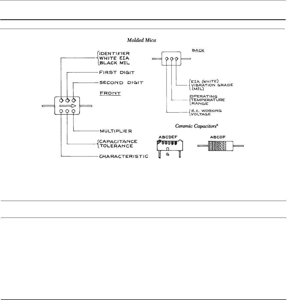
Table 6.7 Capacitor coding
Color Significant
Digits
Multiplier Capacitance
Tolerance (%)
d.c. Working
Voltage
Operating
Temperature (°C)
EIA/Vibration
Black 0 1 — — 55 to +70 10 to 55 Hz
Brown 1 10 61 100 — —
Red 2 100 62—55 to +85 —
Orange 3 1 000 — 300 — —
Yellow 4 10 000 — — 55 to +125 10 to 2000 Hz
Green 5 — 65 500 — —
Blue 6 — — — 55 to +150 —
Violet 7 — 67—— —
Gray 8 — — — — —
White 9 — 69 — — EIA
Gold — — 65 1000 — —
Silver — — 610 — —
Equivalences:
10
6
F ¼1 lF, 1 MFD.
10
9
F ¼0.001 lF, 1 gF, 1000 pF.
10
12
F ¼0.001 gF, 1 pF, 1 MMFD, 1 llF.
Table 6.7 Capacitor coding
PASSIVE COMPONENTS 387

Trimmers are used to compensate for the tolerance and
variation of fixed components. They are not designed for
continuous adjustment, 200 cycles is their design life. The
resistance elements are carbon composition, cermet, or
wire. They can be single-turn or have multiturn lead screws
or worm gears.
6.2.3 Transmission Lines
The most common transmission lines are those with two
conductors. A number of common configurations are
shown in Figure 6.27. Common VHF flat television antenna
le
ad-in cable is an example of a two-wire transmission line.
RG/U cables found in almost all laboratories are examples
Table 6.7 (cont.)
Six Dot or Six-Band Code
a
Five-Dot or Five-Band Code
a
A and B (when marked) temperature coefficient A and B (when marked) temperature coefficient
C first significant figure C first significant figure
D second significant figure D second significant figure
E decimal multiplier E decimal multiplier
F military code number
Temperature Characteristics
A B Temp. Coeff.
b
A B Temp. Coeff.
b
ppm/°C
Gray Black Gen. Purpose Black — NP0 0
Orange Orange N 1500 Brown — N030 30
Yellow Orange N 2200 Red — N080 80
Green Orange N 3300 Orange — N150 150
Blue Orange N 4700 Yellow — N220 220
Red Violet P100 Green — N330 330
Green Blue P030 Blue — N470 470
Gold Orange X5F Violet — N750 750
Brown Orange Z5F Gold — P100 +100
Gold Yellow X5P White —
Brown Yellow Z5P Gray —
Gold Blue X5S
Brown Blue Z5S
Gold Gray X5U
Brown Gray Z5U
388 ELECTRONICS

of coaxial transmission lines – such coaxial cable is also
used for UHF and satellite television leads. The wire-and-
plane configuration is less common. The ribbon-and-plane
configuration occurs very often in printed circuit boards
(PCBs), where the ribbon is the metal trace on one side
of the board and the plane is a continuous conducting sheet
on the opposite side, often called the ground plane. A trans-
mission line of this type is called a microstrip line. The
formulae for the characteristic impedance Z
0
of the geo-
metries in Figure 6.27 are given in Table 6.9.
The
properties of a transmission line are given in terms
of the series impedance Z and shunt admittance Y per unit
length:
Z ¼ R þ jxL
Y ¼ G þ jxC
ð6:30Þ
where j ¼
ffiffiffiffiffiffiffi
1
p
and G is the shunt cond uctance, which is the
reciprocal of the shunt resistance per unit length. The charac-
teristic impedance Z
0
is
ffiffiffiffiffiffiffiffiffi
Z=Y
p
. Voltage and current propa-
gate along a transmission line as waves. The properties of the
waves are determined by the propagation constant c and phase
velocity v
p
.Theyaregivenbyc ¼
ffiffiffiffiffiffi
ZY
p
¼ a þ jb and v
p
¼
x/b,wherex is the frequency of the wave. The wav elength in
the transmission line is k ¼ 2pv
p
/x ¼ 2p/b. The attenuation
of the wave is given by the factor e
a
per unit length. These
formulae are summarized in Table 6.10. For most practical
t
ransmission lines, the series resistance per unit length R is
small compared to the inductiv e reactance xL, and the shunt
conductance G is small compared to the reciprocal of the
capacitance reactance 1/xC. Under these conditions, Z
0
is
essentially
ffiffiffiffiffiffiffiffiffi
L=C
p
, a becomes [R/Z
0
þ GZ
0
]/2, and b
becomes x
ffiffiffiffiffiffi
LC
p
. The phase velocity is independent of
frequency and is the ratio of the speed of light in
Table 6.7 (cont.)
Capacitance
Color Digit (C and D) Multiplier (E) Nominal Capacitance
< 10 pF > 10 pF
Black 0 1 62.0 pF 620%
Brown 1 10 60.1 pF 61%
Red 2 100 — 62%
Orange 3 1 000 — 6 3%
Yellow 4 10 000 +100%, 0%
Green 5 — 60.5 pF 65%
Blue 6 — — —
Violet 7 — — —
Gray 8 0.01 60.2 pF +80%, to 20%
White 9 0.1 61.0 pF 610%
a
Nominal capacitance code is EIA-RS 198.MIL-SPEC code not the same. Five- and six-digit codes are both used for radial-lead and
axial-lead capacitors. Disc capacitors normally have typographical marking but may be color-coded.
b
N designates a negative temperature coefficient; P designates a positive temperature coefficient.
PASSIVE COMPONENTS 389

vacuum to the square root of the dielectric constant,
e, of the mat erial separating the conductors. For reason-
able values of con duc tor geomet ry, Z
0
lies approximately
between 50 and 500 ohms. The attenuation a is obtained
from the shunt conductance G and series resist ance R,
once Z
0
is known. For most dielectrics, G is very small
(for air, G can be taken equal to z ero) and R becomes the
dominant factor. Because of the skin effect, R increases
with frequency ( see Table 6.1). The properties of common
coax
ial cables are giv en in Table 6.11. Attenuation ratings
f
or RG/U cables as a function of frequency are given in Table
6.1
2. along with jacket information. As is to be expected, the
Table 6.8 Surface-mount (SMT) codes
SMT Resistor Tolerance Code
Letter Tolerance
D 60.5%
F 61.0%
G 62.0%
J 65.0%
SMT Capacitor Significant Figure Code
Character Figures Character Figures Character Figures
A 1.0 N 3.3 a 2.5
B 1.1 P 3.6 b 3.5
C 1.2 Q 3.9 d 4.0
D 1.3 R 4.3 e 4.5
E 1.5 S 4.7 f 5.0
F 1.6 T 5.1 m 6.0
G 1.8 U 5.6 n 7.0
H 2.0 V 6.2 t 8.0
J 2.2 W 6.8 y 9.0
K 2.4 X 7.5
L 2.7 Y 8.2
M 3.0 Z 9.1
SMT Capacitor Code
Character Multiplier
01
110
2 100
3 1 000
4 10 000
5 100 000
6 1 000 000
7 10 000 000
8 100 000 000
9 0.1
390 ELECTRONICS
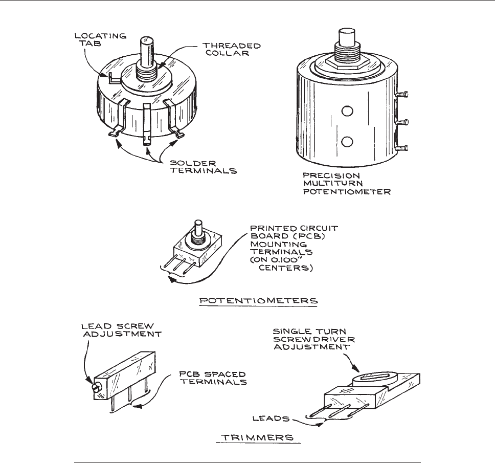
smaller cables show greater attenuation due to the neces-
sity of using a small-diameter inner conductor to maintain
a reasonable ratio of outer to inner conductor diameter.
The most common cable has a characteristic impedance
of 50 ohms. Twisted pairs of s ingle-conductor wire a re
used where immunity from noise is important. Unwanted
signals induc ed in both conductors can be canceled elec-
tronically by differential amplification.
As a general rule, at least one end of a transmission line
should be terminated with a resistance equal to Z
0
to pre v ent
ringing and undesirable reflections if the line is used for
sending signals over distances greater than k/8. The trans-
mission of pulses with nanosecond rise times over distances
of a fe w centimeters on a printed circuit board, for example,
requires termination. In theory, termination of the source or
load end of the line is sufficient. In practice, howe ver, it is
Figure 6.26 Some common types of variable resistors.
PASSIVE COMPONENTS 391
usually the load end that is ter minated. Because 50 ohms
cable is so common, electronic instruments designed to oper-
ate at high frequencies often have 50 ohms input and output
impedances to facilitate connections. Such low-impedance
instruments are not suitable for use in combination with
lower -frequenc y devices, which may be seriously over-
loaded by 50 ohms.
The velocity of propagation v
p
of an electrical signal
through a transmission line is 1=
ffiffiffiffiffiffiffi
LC
p
¼ Z
0
=L ¼ 1=Z
0
C.
For 50 ohms cable with a polyethylene or TeflonÔ
Table 6.9 Characteristic impedance of
transmission-line geometries
Geometry Z
0
(X)
a
Two-wire
138
ffiffi
e
p
ln
b
a
Coaxial
276
ffiffi
e
p
ln
b
a
Wire and plane
60
ffiffi
e
p
ln
4h
d
Ribbon and plane
or Microstrip line
b
87
ffiffiffiffiffiffiffiffiffiffiffiffiffiffiffiffiffi
e þ 1:41
p
ln
5:98h
0:8wþt
Twisted pair (AWG
24–28, 30 turns/f.)
110
Strip line
b
60
ffiffi
e
p
ln
4b
0:67pwð0:8þtwÞ
a
e ¼1.0 for air and 5.0 for G-10 fiberglass epoxy circuit board.
b
Copper foil thickness is 0.001 in. for 1 oz cladding and 0.002 in.
for 2 oz cladding.
Table 6.10 General transmission-line properties
Quantity Symbol Relation to Fundamental
Parameters
Shunt admittance YG+ j x C
Series impedance ZR+ j x L
Characteristic impedance Z
0
ffiffiffiffiffiffiffiffiffi
Z=Y
p
Wavelength k 2 p/b
Propagation velocity v
p
c=
ffiffi
e
p
Attenuation constant a ½R=Z
0
+ GZ
0
=2
Propagation constant c
ffiffiffiffiffiffi
ZY
p
¼ a þ jb
Figure 6.27 Fixed-geometry transmission-line configurations.
392 ELECTRONICS

Table 6.11 Properties of coaxial cable
Military RG
Number
Armor
O.D.
(in.)
Jacket
O.D.
(in.)
Jacket
Type
a
Dielectric
O.D. (in.)
Dielectric
Type
b
Center
Conductor
c
V.P.
d
(%) Capacitance
(pF/ft.)
Max. RMS
Operating
Voltage (V)
Nominal
Impedance
(X)
5B — 0.328 IIa .181 P 16 S 65.9 28.5 3 000 50
6A/U — 0.332 IIa .185 P 21 CW 65.9 20 2 700 75
7A/U — 0.405 I .285 P 7/21 C 65.9 29.5 5 000 52
8A/U — 0.405 IIa .285 P 7/21 C 65.9 29.5 5 000 52
9 — 0.420 II Gray .280 P 7/21 S 65.9 30 5 000 51
9A — 0.420 II Gray .280 P 7/21 S 65.9 30 5 000 51
9B/U — 0.420 IIa .280 P 7/21 S 65.9 30 5 000 50
10A/U 0.475 0.405 IIa .285 P 7/21 C 65.9 29.5 5 000 52
11A — 0.405 I .285 P 7/26 TC 65.9 20.5 5 000 75
11A/U — 0.405 IIa .285 P 7/26 TC 65.9 20.5 5 000 75
12A/U 0.475 0.405 IIa .285 P 7/26 TC 65.9 20.5 5 000 75
13 — 0.420 I .280 P 7/26 TC 65.9 20.5 5 000 74
13A/U — 0.420 IIa .280 P 7/26 T 65.9 20.5 5 000 74
14A/U — 0.545 IIa .370 P 10 C 65.9 29.5 7 000 52
17A — 0.870 IIa .680 P .188 C 65.9 29.5 11 000 52
17A/U — 0.870 IIa .680 P .188 C 65.9 29.5 11 000 52
18A/U 0.945 0.870 IIa .680 P .188 C 65.9 29.5 11 000 52
19A/U — 1.120 IIa .910 P .250 C 65.9 29.5 14 000 52
20A/U 1.195 1.120 IIa .910 P .250 C 65.9 29.5 14 000 52
21A — 0.332 IIa .185 P 16 N 65.9 29 2 700 53
22 — 0.405 I .285 P Two 7/.0152 C 65.9 16 1 000 95
22B/U — 0.420 IIa .285 P# Two 7/.0152 C 65.9 16 1 000 95
34B/U — 0.630 IIa .460 P 7/.0249 C 65.9 21.5 6 500 75
35B/U 0.945 0-870 IIa .680 P .1045 C 65.9 21 10 000 75
55B/U — 0.206 IIIa .116 P 20 S 65.9 28.5 1 900 53.5
57A/U — 0.625 IIa .472 P Two 7/21 C 65.9 16 3 900 95
58/U — 0.195 I .116 P 20 C 65.9 28.5 1 900 53.5
58A/U — 0.195 I .116 P 19/.0071 TC 65.9 30 1 900 50
58C/U — 0.195 IIa .116 P 19/.0071 TC 65.9 30 1 900 50
59/U — 0.242 I .146 P 22 CW 65.9 21.5 2 300 73
59B/U — 0.242 IIa .146 P .023 CW 65.9 21 2 300 75
62/U — 0.242 I .146 SSP 22 CW 84 13.5 750 93
62A/U — 0.242 IIa .146 SSP 22 CW 84 13.5 750 93
62B/U — 0.242 IIa .146 SSP 7/32 CW 84 13.5 750 93
63/U — 0.405 I .285 SSP 22 CW 84 10 1 000 125
PASSIVE COMPONENTS 393

Table 6.11 (cont.)
Military RG
Number
Armor
O.D.
(in.)
Jacket
O.D.
(in.)
Jacket
Type
a
Dielectric
O.D. (in.)
Dielectric
Type
b
Center
Conductor
c
V.P.
d
(%) Capacitance
(pF/ft.)
Max. RMS
Operating
Voltage (V)
Nominal
Impedance
(X)
63B/U — 0.405 IIa .285 SSP 22 CW 84 10 1 000 125
71A — < 0.250 I .146 SSP 22 CW 84 13.5 750 93
71B/U — 0.250 IIIa .146 SSP 22 CW 84 13.5 750 93
74A/U 0.615 0.545 IIa .370 P 10 C 65.9 29.5 7 000 52
79B/U 0.475 0.405 IIa .285 SSP 22 CW 84 10 1 000 125
87A/U — 0.425 V .280 TF 7/20 S 69.5 29.5 5 000 50
108A/U — 0.235 IIa .079 ea. P Two 7/28 TC 68 23.5 1 000 78
111A/U 0.490 0.420 IIa .285 P Two 7/.0152 C 65.9 16 1 000 95
114/U — 0.405 I .285 SSP 33 CW 88 6.5 1 000 185
114A/U — 0.405 IIa .285 SSP 33 CW 88 6.5 1 000 185
115 — 0.375 V .250 #IT 7/21 S 70 29.5 5 000 50
115A/U — 0.415 V .250 #IT 7/21 S 70 29.5 4 000 50
116/U 0.475 0.425 V .280 TF 7/20 S 69.5 29.5 5 000 50
122/U — 0.160 IIa .096 P 27/37 TC 65.9 29.5 1 900 50
140/U — 0.233 V .146 TF .025 SCW 69.5 21 2 300 75
141/U — 0.190 V .116 TF .0359 SCW 69.5 28.5 1 900 50
141A/U — 0.190 V .116 TF# .039 SCW 69.5 28.5 1 900 50
142/U — 0.206 V .116 TF# .0359 SCW 69.5 28.5 1 900 50
142/B — 0.195 IX .116 TF .039 SCW 69.5 28.5 1 900 50
143 — 0.325 V .185 TF .057 SCW 69.5 28.5 3 000 50
142A/U — 0.206 V .116 TF .039 SCW 69.5 28.5 1 900 50
143A/U — 0.325 V .185 TF .059 SCW 69.5 28.5 3 000 50
149/U — 0.405 I .285 P 7/26 TC 65.9 20.5 5 000 75
164/U — 0.870 IIa .680 P .1045 C 65.9 21 10 000 75
174/U — 0.100 I .060 P 7/.0063 CW 65.9 30 1 500 50
178B/U — 0.075 VII .034 TF 7/38 SCW 69.5 29.0 1 000 50
179B/U — 0.105 VII .063 TF# 7/38 SCW 69.5 19.5 1 200 75
180B/U — 0.145 VII .102 TF 7/38 SCW 69.5 15.0 1 500 95
187/U — 0.110 VII .063 TF 7/38 SCW 69.5 19.5 1 200 75
188/U — 0.110 VII .060 TF 7/.0067 SCW 69.5 29 1 200 50
195/U — 0.155 VII .102 TF 7/38 SCW 69.5 15 1 500 95
196/U — 0.080 VII .034 TF 7/38 SCW 69.5 29 1 000 50
209/U — 0.745 VI .500 SST 19/.0378 S 84 26.5 3 200 50
210/U — 0.242 V .146 SST 22 SCW 84 13.5 750 93
211A/U — 0.730 V .620 TF .190 C 69.5 29.0 7 000 50
394 ELECTRONICS

insulation, v
p
is of the order of 2 3 10
10
m/s, which gives a
delay of 5 ns /m. For delays up to a few hundre d nano-
seconds, high-quality, low-loss coaxial cable provides an
excellent delay line, because no distortion of the propa-
gated signal occurs w hen it is properly terminated. The
best cabl e to use for critical delay-line applications is
rigid or semirigid air-core coaxial cable. With air as the
dielectric, the shunt conductance is virtually zero. Semi-
rigid construction assures that the coaxial geometry is
maintained within tight tolerances, reducing distortion.
Such cable is practical for use at frequencies up to the
microwave region.
Table 6.11 (cont.)
Military RG
Number
Armor
O.D.
(in.)
Jacket
O.D.
(in.)
Jacket
Type
a
Dielectric
O.D. (in.)
Dielectric
Type
b
Center
Conductor
c
V. P.
d
(%) Capacitance
(pF/ft.)
Max. RMS
Operating
Voltage (V)
Nominal
Impedance
(X)
212/U — 0.332 IIa .185 P .0556 S 65.9 28.5 3 000 50
213/U — 0.405 IIa .285 P 7/.0296 C 65.9 29.5 5 000 50
214/U — 0.425 IIa .285 P 7/.0296 S 65.9 30 5 000 50
215/U 0.475 0.405 IIa .285 P 7/.0296 C 65.9 29.5 5 000 50
216/U — 0.425 IIa .285 P 7/26 TC 65.9 20.5 5 000 75
217/U — 0.545 IIa .370 P .106 C 65.9 29.5 7 000 50
218/U — 0.870 IIa .680 P .195 C 65.9 29.5 11 000 50
219/U 0.945 0.870 IIa .680 P .195 C 65.9 29.5 11 000 50
220/U — 1.120 IIa .910 P .260 C 65.9 29.5 14 000 50
221/U 1.195 1.120 IIa .910 P .260 C 65.9 29.5 14 000 50
222/U — 0.322 IIa .185 P .0556 N 65.9 29 2 700 50
223/U — 0.216 IIa .116 P .035 S 65.9 29.5 1 900 50
225/U — 0.430 V .285 TF 7/.0312 S 69.5 29.5 5 000 50
227/U 0.490 0.430 V .285 TF 7/.0312 5 69.5 29.5 5 000 50
228A/U 0.795 0.730 V .620 TF .190 C 69.5 29.0 7 000 50
264/U — 0.750 PU .176 P Four 19/27 C 69.5 40.0 N.A. 40
280/U — 0.480 IX .327 TT 9C 80 27 3 000 50
281/U — 0.750 VI .500 TT 19/.0378 S 80 27 3 200 50
301/U — 0.245 IX .185 TF 7/.0203 K 69.5 28.5 3 000 50
302/U — 0.206 IX .146 TF 22 SCW 69.5 21 2 300 75
303/U — 0.170 IX .116 TF .038 SCW 69.5 28.5 1 900 50
304/U — 0.280 IX .185 TF .059 SCW 69.5 28.5 3 000 50
307A/U — 0.270 IIIa .146 SSP 19/.0058 S 80.0 17 N.A. 75
316/U — 0.102 IX .060 TF 7/.0067 SCW 69.5 29 1 200 50
a
Designation listed at end of this table.
b
P: polyethylene; SSP: semisolid polyethylene; TF: Teflon; TT: Teflon tape; SST: semisolid Teflon.
c
Number of strands, gauge (B&S) or O.D., and material are specified. A single solid wire results in the lowest cable attenuation.
Stranding increases flexibility. S: silvered copper; C: copper; TC: tinned copper; N: Nichrome; CW: Copperweld; SCW: silvered
Copperweld; K: Karma.
d
100% x (velocity of propagation)/(velocity in vacuum).
PASSIVE COMPONENTS 395

For longer delays, lumped-element delays are the most
practical. These delays consist of low-pass filter sections
connected in series. For frequencies below their corner
frequency, they act as delay lines. The number of sections
n required is related to the ratio of the delay time t
d
to the
rise time t
r
, and is given by n ¼ 1.5 t
d
/t
r
. The incorporation
of multiple taps between the sections allows a choice of
delays with a single unit.
For a line le ngth less than a quarter wavelength, a
transmission line behaves like a capacitor or an inductor,
depending on whether the end of the line is an open
circuit or s hort circ uit. A line that is a n odd number
of quarter-wavelengths long behaves like a parallel res-
onant RLC circuit when short-circuited at one end, and
like a series resonant circuit when open-circuited.
The Qs of such resonant circuits are much higher than
attainable with lumped elements. There are, however, an
infinite number of resonance s corresponding to frequen-
cies where:
v
p
=f ¼ð2n +1Þk=4
where n is an integer.
TABLE 6.12 Properties of coaxial cable
Attenuation ratings for RG/U cable
Nominal Attenuation [dB/(100 ft)]
Frequency (MHz): 1.0 10 50 100 200 400 1000 3000 5000 10 000
RG/U Type
5, 5A, 5B, 6, 6A, 212 0.26 0.83 1.9 2.7 4.1 5.9 9.8 23.0 32.0 56.0
7 0.18 0.64 1.6 2.4 3.5 5.2 9.0 18.0 25.0 43.0
8, 8A, 10, 10A, 213, 215 0.15 0.55 1.3 1.9 2.7 4.1 8.0 16.0 27.0 >100.0
9, 9A, 9B, 214 0.21 0.66 1.5 2.3 3.3 5.0 8.8 18.0 27.0 45.0
11, 11A, 12, 12A, 13, 13A, 216 0.19 0.66 1.6 2.3 3.3 4.8 7.8 16.5 26.5 > 100.0
14, 14A, 74, 74A, 217, 224 0.12 0.41 1.0 1.4 2.0 3.1 5.5 12.4 19.0 50.0
17, 17A, 18, 18A, 177, 218, 219 0.06 0.24 0.62 0.95 1.5 2.4 4.4 9.5 15.3 > 100.0
19, 19A, 20, 20A, 220, 221 0.04 0.17 0.45 0.69 1.12 1.85 3.6 7.7 11.5 > 100.0
21, 21A, 222 1.5 4.4 9.3 13.0 18.0 26.0 43.0 85.0 > 100.0 > 100.0
22, 22B, 111, 111A 0.24 0.80 2.0 3.0 4.5 6.8 12.0 25.0 > 100.0 > 100.0
29 0.32 1.20 2.95 4.4 6.5 9.6 16.2 30.0 44.0 > 100.0
34, 34A, 34B 0.08 0.32 0.85 1.4 2.1 3.3 5.8 16.0 28.0 > 100.0
35, 35A, 35B, 164 0.08 0.08 0.58 0.85 1.27 1.95 3.5 8.6 15.5 > 100.0 > 100.0
54, 54A 0.33 0.92 2.15 3.2 4.7 6.8 13.0 25.0 37.0 > 100.0
55, 55A, 55B, 223 0.03 0.30 1.2 3.2 4.8 7.0 10.0 16.5 30.5 46.0 > 100.0
57, 57A, 130, 131 0.18 0.65 1.6 2.4 3.5 5.4 9.8 21.0 > 100.0 > 100.0 > 100.0
58, 58B 0.33 1.25 3.15 4.6 6.9 10.5 17.5 37.5 60.0 > 100.0
58A, 58C 0.44 1.4 3.3 4.9 7.4 12.0 24.0 54.0 83.0 > 100.0
59, 59A, 59B 0.33 1.1 2.4 3.4 4.9 7.0 12.0 26.5 42.0 > 100.0
62, 62A, 71, 71A, 71B 0.25 0.85 1.9 2.7 3.8 5.3 8.7 18.5 30.0 83.0
62B 0.31 0.90 2.0 2.9 4.2 6.2 11.0 24.0 38.0 92.0
63, 63B, 79, 79B 0.19 0.52 1.1 1.5 2.3 3.4 5.8 12.0 20.5 44.0
87A, 116, 165, 166, 225, 227 0.18 0.60 1.4 2.1 3.0 4.5 7.6 15.0 21.5 36.5
94 0.15 0.60 1.6 2.2 3.3 5.0 7.0 16.0 25.0 60.0
94A, 226 0.15 0.55 1.2 1.7 2.5 3.5 6.6 15.0 23.0 50.0
396 ELECTRONICS

Jacket Type
Designation Material Temperature Limits (°C)
Type I Black polyvinyl chloride 40 to þ80
Type IIa Black polyvinyl chloride
(noncontaminating):
<1=4 in. 55 to þ80
>1=4 in. 40 to þ80
Type IIIa Black polyethylene 55 to þ85
Type IV Black synthetic rubber:
<1=2 in. 55 to þ80
>1=2 in. 40 to þ80
Type V Fiber glass 55 to þ250
Type VI Silicone rubber 55 to þ175
Type VII Polytetrafluoroethylene (Teflon) 55 to þ200
Type IX Fluorinated Ethylene Propylene (FEP) 55 to þ200
PU Polyurethane (Estane) 60 to þ180
Table 6.12 (cont.)
Nominal Attenuation [dB/(100 ft)]
Frequency (MHz): 1.0 10 50 100 200 400 1000 3000 5000 10 000
108, 108A 0.70 2.3 5.2 7.5 11.0 16.0 26.0 54.0 86.0 > 100.0
114, 114A 0.95 1.3 2.1 2.9 4.4 6.7 11.6 26.0 40.0 65.0
115, lISA, 235 0.17 0.60 1.4 2.0 2.9 4.2 7.0 13.0 20.0 33.0
117, 118, 211, 228 0.09 0.24 0.60 0.90 1.35 2.0 3.5 7.5 12.0 37.0
119, 120 0.12 0.43 1.0 1.5 2.2 3.3 5.5 12.0 17.5 54.0
122 0.40 1.7 4.5 7.0 11.0 16.5 29.0 57.0 87.0 > 100.0
125 0.17 0.50 1.1 1.6 2.3 3.5 6.0 13.5 23.0 > 100.0
140, 141, 141A 0.30 0.90 2.1 3.3 4.7 6.9 13.0 26.0 40.0 90.0
142, 142A, 142B 0.34 1.1 2.7 3.9 5.6 8.0 13.5 27.0 39.0 70.0
143, 143A 0.25 0.85 1.9 2.8 4.0 5.8 9.5 18.0 25.5 52.0
144 0.19 0.60 1.3 1.8 2.6 3.9 7.0 14.0 22.0 50.0
149, 150 0.24 0.88 2.3 3.5 5.4 8.5 16.0 38.0 65.0 > 100.0
161, 174 2.3 3.9 6.6 8.9 12.0 17.5 30.0 64.0 99.0 > 100.0
178, 178A, 196 2.6 5.6 10.5 14.0 19.0 28.0 46.0 85.0 > 100.0 > 100.0
179, 179A, 187 3.0 5.3 8.5 10.0 12.5 16.0 24.0 44.0 64.0 > 100.0
180, 180A, 195 2.4 3.3 4.6 5.7 7.6 10.8 17.0 35.0 50.0 88.0
188, 188A 3.1 6.0 9.6 11.4 14.2 16.7 31.0 60.0 82.0 > 100.0
209 0.08 0.27 0.68 1.0 1.6 2.5 4.4 9.5 15.0 48.0
281 0.09 0.32 0.78 1.1 1.7 2.5 4.5 9.0 13.0 24.0
PASSIVE COMPONENTS 397
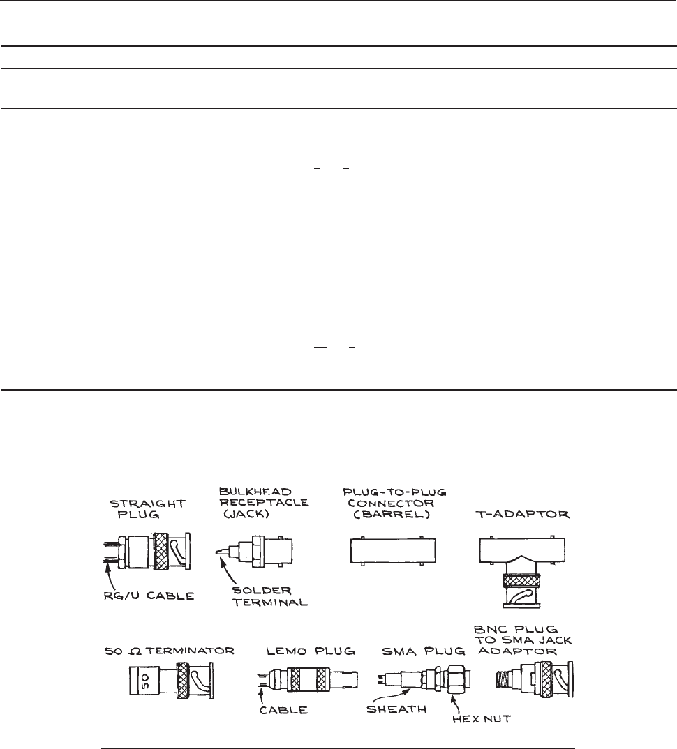
Table 6.13 Common coaxial connector types
Size Classification Connector Type Attachment Method Cable Size
Range (in.)
Maximum Frequency
(GHz)
RMS Working
Voltage (V)
Medium UHF Screw
3
16
to
7
8
0.5 500
N
C
SC
Screw
Bayonet
Screw
9
=
;
3
8
to
7
8
11
1,000
1,500
1,500
7-mm precision Sexless Screw .141, .250, .325,
semirigid; RG 214/U, RG
142B/U
18 1,500
Miniature
BNC
MHV
a
TNC
Bayonet
Bayonet
Screw
9
=
;
1
8
to
3
8
4
4
11
8
<
:
500
5,000
500
SHV Bayonet 0.080 to 0.420 — 10,000 d.c.
b
Subminiature
SMB
SMC
SMA
Snap on
Screw
Screw
9
=
;
1
16
to
1
8
3
10
18
8
<
:
500
500
350
LEMO
c
Push on 0.100 to 0.195 4 1,500
a
Higher-voltage version of the BNC connector, not mateable with BNC connectors.
b
NIM high-voltage connector.
c
00 shell size. Manufactured in the United States as K-Loc by Kings Electronics Co.
Source: Reference 2.
Figure 6.28 Some coaxial connectors.
398 ELECTRONICS
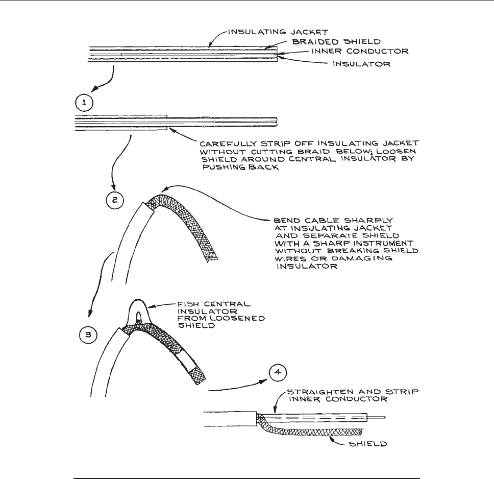
6.2.4 Coaxial Connectors
Probably more time is spent with connectors than with any
other element of electronic hardware. When deciding on
the method of connecting various pieces of electronic
equipment, it is wise to be aware of the variety of connec-
tors available and choose a family of connectors best
suited to the task. In many cases, the choice of connector
is dictated by the connectors at the outputs and inputs of
existing equipment.
Figure 6.29(a) Procedure for stripping coaxial cables; Assembly procedure for BNC/MHV
ferrule-clamp connector.
PASSIVE COMPONENTS 399
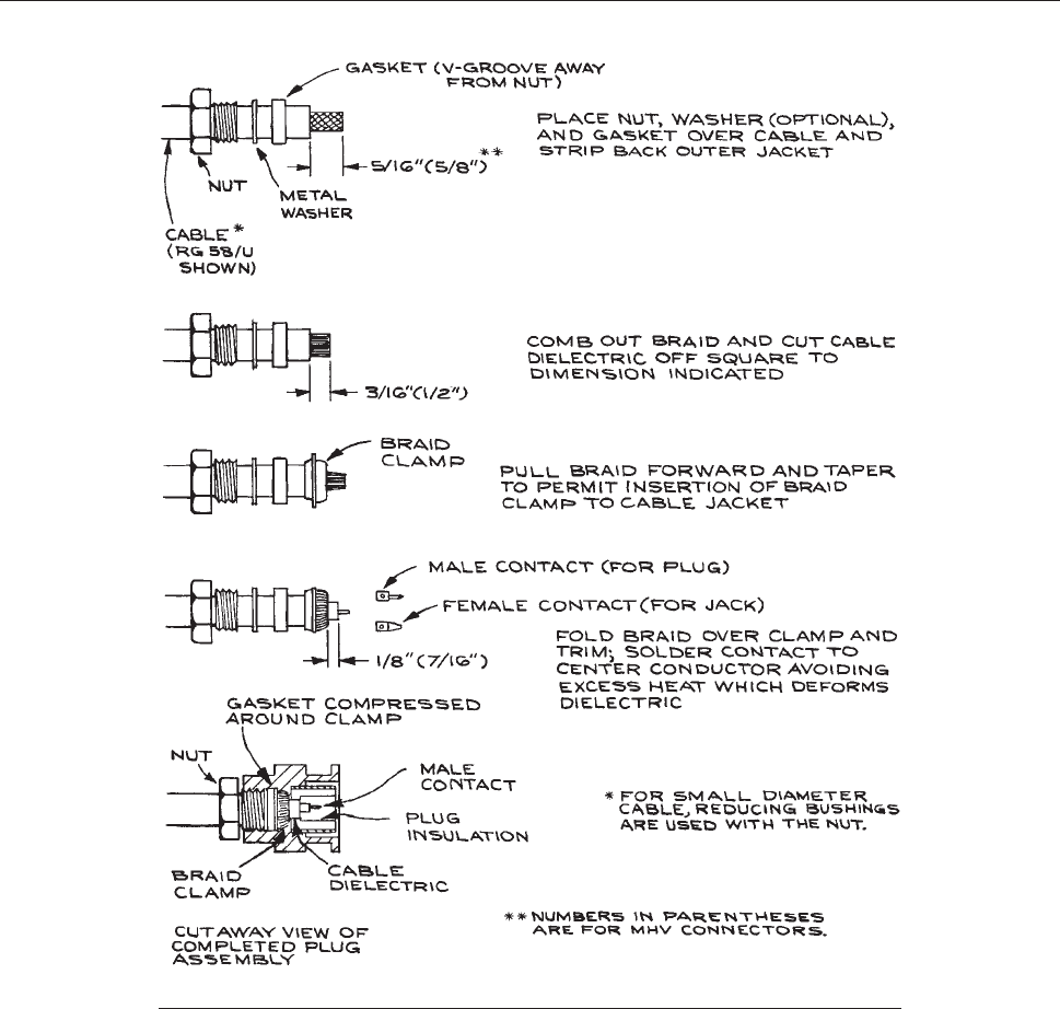
The most common connector is currently the BNC. It is
a miniature bayonet type, but circuit density has increased
enormously with the extensive use of integrated circuits
and the BNC connector is now being replaced by a variety
of subminiature connectors – among which the LEMOÔ
has taken the lead for nuclear instrumentation. A list of
common coaxial connectors is given in Table 6.13.
In
addition to coaxial connector plugs, each series of con-
nectors has a wide variety of jacks and adaptors (generally
plug refers to the connector attached to the cable or wire,
while jack refers to the connector to which the plug mates).
Jacks for chassis mounting, bulkhead mounting, and
printed circuit-board mounting are available, as well as
hermetically seal ed jacks for making coaxial connections
Figure 6.29(b)
400 ELECTRONICS
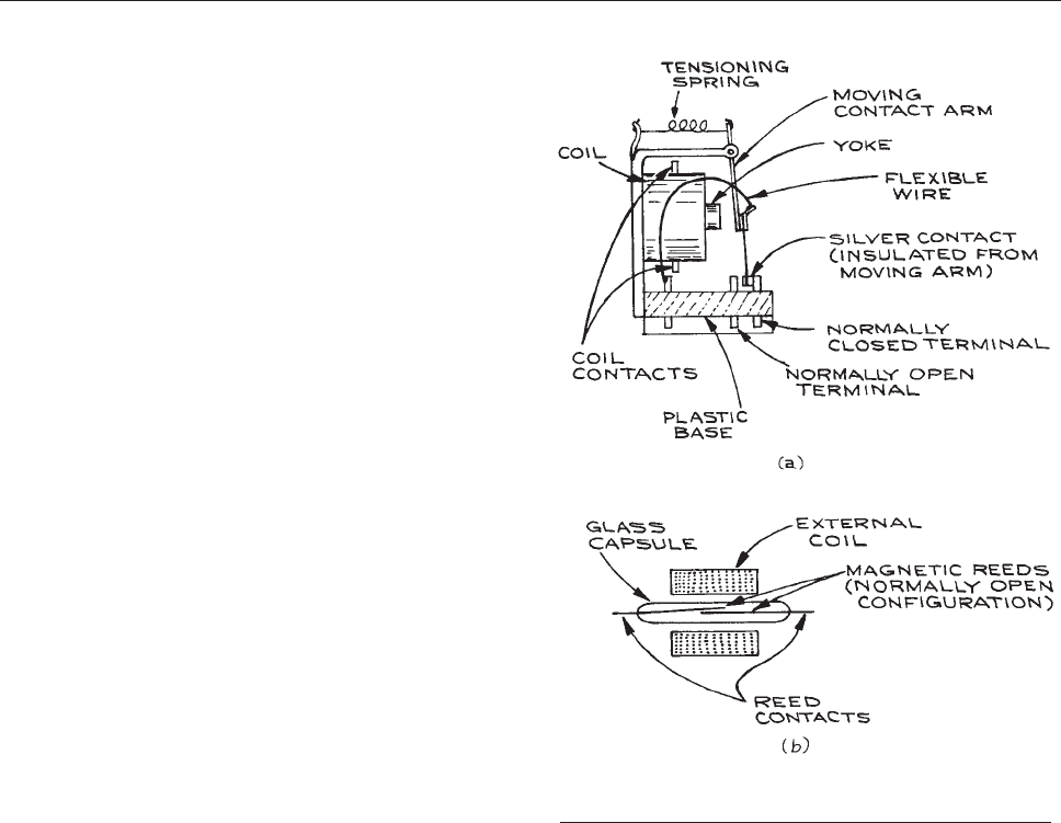
through a vacuum wall. Tees and barrels allow o ne to
connect cables together and there are terminators that
can be attached directly to input or output jacks. In addi-
tion, each series has a certain number of interseries adap-
tors for connection of plugs or jacks to those of other
series. Some of the different connectors ar e shown in
Figure 6.28. It is advisable to reduce the number of adap-
tors
to a mini mum to maintain the transmission-line prop-
erties of the connections with a s few reflecti on-producing
discontinuities as possible.
A good connector should be easy to fit to the proper
cable and should not introduce any discontinuities in
the transmission-line properties of the cable. Needless to
say, the characteristic impedance of the connector should
be identical to that of the cable. The connector should be a
strong mechanical fit to the cable, and it should be easy to
connect and disconnect from mating connectors.
Any given connector type comes in a variety of styles to
accommodate different cable sizes. Configurations – such as
straight and right angle – are available, and often there are
different choices for the mechanical and electrical connec-
tions of the connector to the cable, the three most common
being a ferrule clamp and screw, crimp, and solder. The pro-
cedure for stripping coaxial cable by hand is shown in Figure
6.
29(a). Shielded lead wire extractors are available for
re
moving insulated lead wire from braided shield. Similar
to a syringe, the extractor removes the lead wire from the
shield leaving the braid intact. Figure 6.29(b) shows the
as
sembly of a ferrule-clamp BNC/MHV connector.
Crimp-style connectors require the use of a special crimping
tool and die. They are stronger, less bulky, more uniform,
and electrically more robust than clamp and solder connec-
tors. Crimping avoids the swelling or melting of the cable
dielectric that can occur when solder-type connectors are
assembled. When attaching connectors to cable, it is highly
recommended that the manufacturer’s cable-cutting proce-
dures be followed so that the inner conductor, insulator,
outer conductor (braid or foil), and outer insulator are of
the proper length. In this way no discontinuities in the elec-
trical properties of the cable are introduced at the cable–
connector interface. Special cutting jigs are available to
assure the proper geometry when preparing the cable for
insertion into the connector.
Assembly instructions for several types of coaxial con-
nectors are given in the Chapter 6 Appendix.
6.2.5 Relays
A relay is an electrically actuated switch. Relay action can
be electromechanical or can be based on solid-state devi-
ces. A large number of contact configurations exist. Impor-
tant parameters are the operating voltage and power rating
of the relay, as well as the contact rating. The speed at
which mechanical relays operate is generally in the 10 to
100 ms range. General-purpose electromagnetic relays
operate at 6, 12, 24, 48, and 110 V d.c. and 6, 12, 24, 48,
110, and 220 V a.c. with coil power ratings of around 1 W
[see Figure 6.30(a)]. Such relays have contacts capable of
Figure 6.30 Mechanical relays: (a) medium-power relay;
(b) reed relay.
PASSIVE COMPONENTS 401
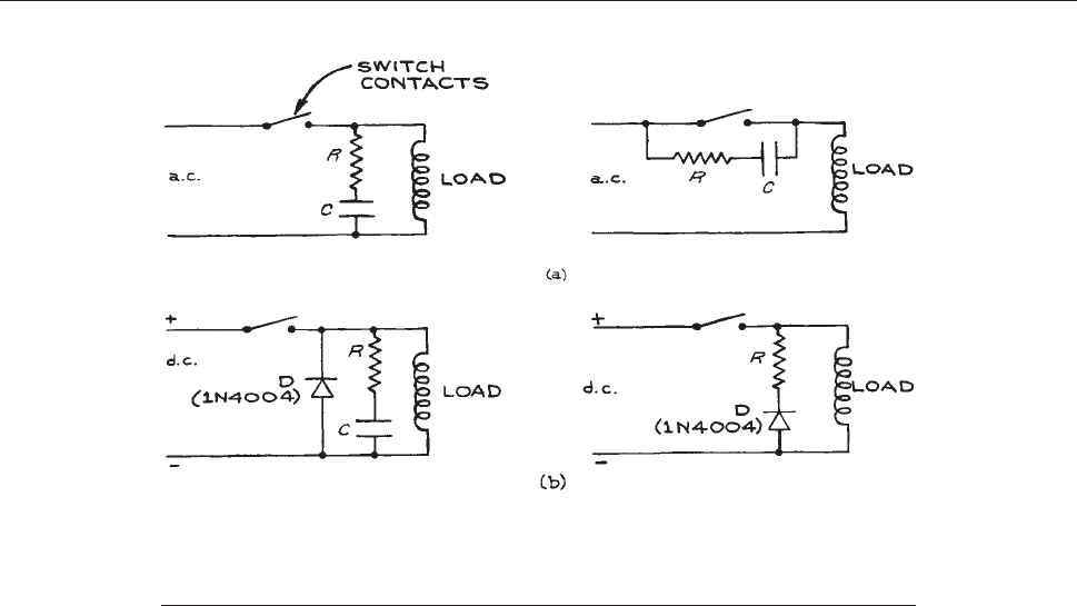
handling from 2 to 10 A. Sensitive mechanical relays use a
large number of turns of fine wire on the electromagnet
coil. They operate with 28 V d.c. and require only 1 to 40
mW of coil power. Contacts are rated from 0.5 to 2 A.
A reed relay is a glass-encapsulated switch having
two flexible thin metal strips , or ree ds, as contact ors.
The switch is placed inside an electromagnetic coil
[Figure 6.30(b)]. The relay contacts can be dry or mer-
cury-wetted.
Standard coil voltages are 6, 12,and24V
d.c., and the coil power is from 50 to 500 mW per reed-
switch capsule. Contacts are rated at 10 mA to 3 A,
depending on size. There is also a maximum open-cir-
cuit voltage that can be sustained by the opened con-
tacts. The low mass of the reeds makes operating times
of 0.2 to 2 ms possible. Small reed relays are made for
PCB mounting.
With inductive loads, the fast opening of relay contacts
can cause a large voltage to appear across them. Some
protective circuits for reducing this problem are illustrated
in Figure 6.31.
Solid-state
relays consi st of a solid-state switching ele-
ment dri v en by an appropriate amplifier. Because the input
circuit is often optically isolated from the load, these relays
introduce little or no noise into the circuit that driv es them.
The load current determines the switching element. Field-
effect transistors (FETs) are used for lo w-level d.c., bipolar
junction transistors (BJTs) for intermediate d.c. currents, and
triacs and silicon-controlled rectifiers (SCRs) for large a.c.
and d.c. currents. Section 6.3 has a discussion of transistors
and
solid-state switches. Though there is no contact wear
with solid-state relays, their on resistance may be large com-
pared with electromechanical devices and they require care-
fully conditioned activating signals. They are much less
tolerant of overload than are electromechanical devices.
6.3 ACTIVE COMPONENTS
The overall properties of semiconductor diodes and tran-
sistors can be understood in terms of the properties of the
Figure 6.31 Contact-conditioning circuits for mechanical relays: (a) a.c. (for small loads
driven from the power line, R ¼ 100 ohms and C ¼ 0.05 lF); (b) d.c. (diodes, D, reduce the
peak voltage from the inductive load and should be able to handle the steady-state current
through the inductor).
402 ELECTRONICS
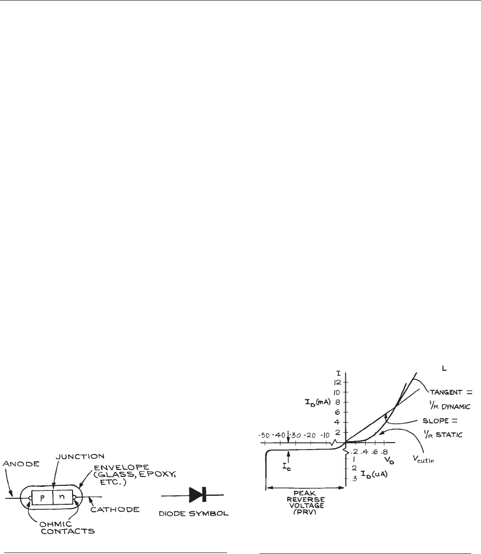
p–n junctions that form them. Without going into a dis-
cussion of solid-state physics, it is sufficient to know that
p-type semiconductor material conducts electricity princi-
pally through the motion of positive charges (holes), while
n-type material owes its conductivity mainly to electrons.
Both p- and n-material can be produced from germanium
or silicon by the addition of impurity atoms – a procedure
called doping.
6.3.1 Diodes
Most semiconductor diodes consist of a p–n junction as
illustrated in Figure 6.32.Theschematicrepresent
ation is
shown next to the simplified drawing of the diode. The
diode is a unidirectio na l d evice: its d.c. current–voltage
(I–V) characteristics depend on the applied potential on
the anode with respect to the cathode. The I–V character-
istics of a typical small-signal silicon diode are drawn in
Figure 6.33. When the anode is p ositive with respect to
the
cathode (forward bias), the d iode conducts a large
current. When the polarity of the applied potential is
reversed (reverse bias), the current i s very small. If the
reverse voltage is increased beyond the peak reverse volt-
age (PRV), br eakd own occurs and the diode conducts
strongly again. Except in the ca se of specially desig ned
Zener diodes, this usually destroys t he diode. The for-
ward-bias voltage at which the diode begins to conduct
strongly is V
cutin
.Forgermaniumdiodes,V
cutin
is 0.2 V,
while for silicon diodes it is 0 .6 V. The I–V characteristics
shown in the g raph are accurately represented by the
formula:
I
d
¼ I
0
e
V
d
=gV
T
1
hi
ð6:31Þ
where I
0
¼ 10
9
A for silicon and 10
6
A for germanium.
I
0
is temperature-dependent, increasing at a rate of 11%/°C
for Ge and 8%/°C for Si. V
T
has the value 0.026 Vat 300 K
and is directly proportional to the absolute temperature,
and g is a unitless constant equal to one for germanium
and two for silicon.
Diodes can be separated into two types according
to the power they can dissipate. Power diodes are used
in high-current applications, for exam ple, as rectifiers in
power supplies. Importa nt specifications for power diodes
are t he maximum forward current, maximum PRV (peak
reverse voltage), and effective forward-bias resistan ce.
Low-power diode s or signal diodes are used to rectify
small signals, mix two frequencies to produce sum a nd
difference frequencies, and switch low voltages and cur-
rents. Besides the current and voltage ratings, the speed
with which diode s can be chan ged from the forward-bias
to the reverse-bia s condition and back is a factor i n hig h-
speed switching circuits. Switching speed is related to the
effective capacitance of the p–n junction. Typical
specifications for a power and signal diode are given in
Tables 6.14 and 6.15.
Man
y older diodes have a 1N-prefix designation.
The two ends of a diode are usually distinguished from
each other by a mark – the cathode end having a black
Figure 6.33 Typical current–voltage characteristics of a
small-signal silicon diode. Note change of vertical and
horizontal scales at the origin.
Figure 6.32 A diode and the corresponding symbol.
ACTIVE COMPONENTS 403
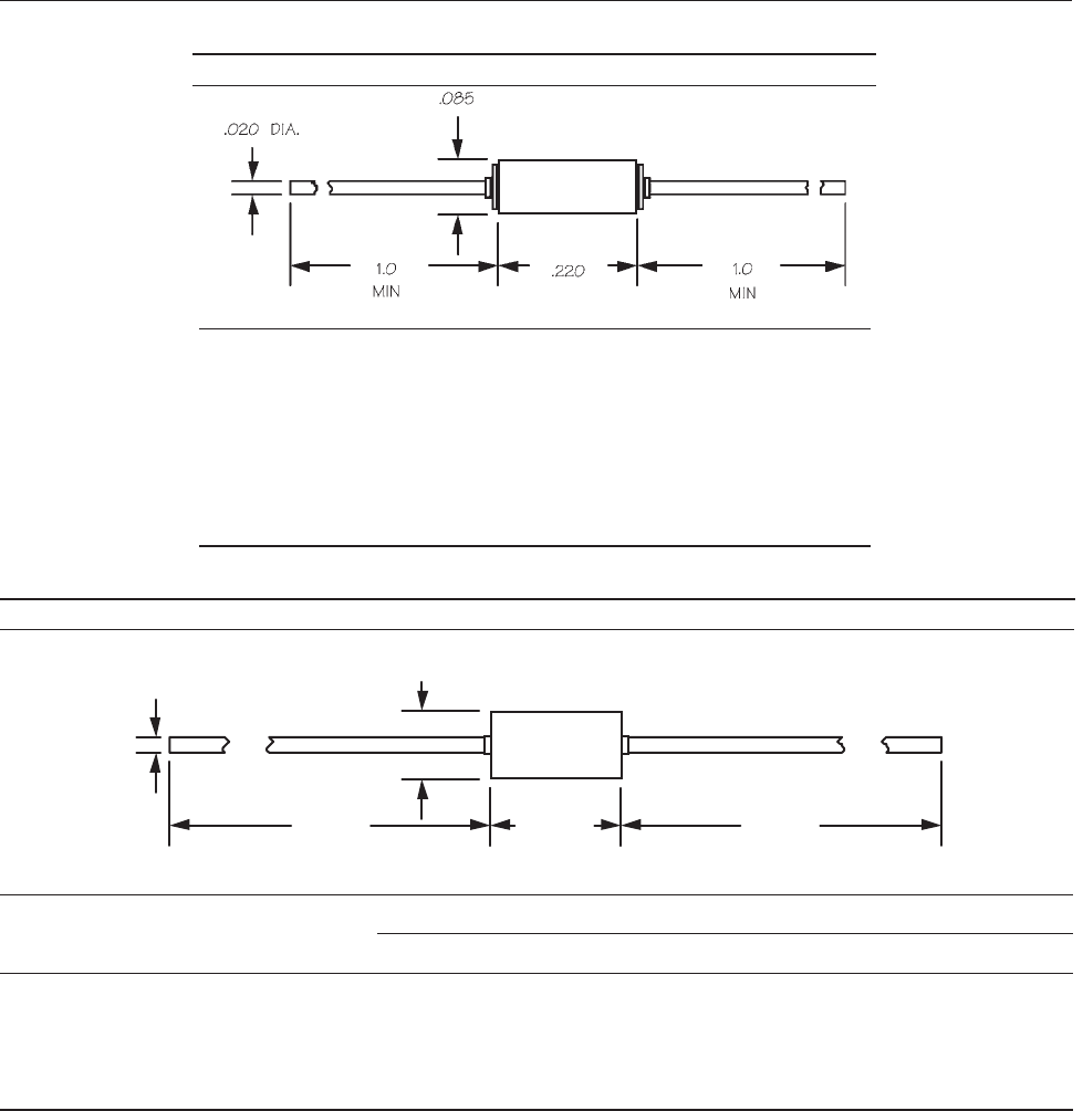
Maximum Ratings
4001 4002 4003 4004 4005 4006 4007
Peak reverse voltage (V) 50 100 200 400 600 800 1000
Non-repetitive peak reverse voltage (V) 50 100 200 400 600 800 1000
Average forward current (A) 1
Peak surge current (1 cycle) (A) 30
Operating temperature range (°C) 65 to +175
1.10
MIN.
.205 1.10
MIN.
.107
.024
DIA.
Table 6.15 Properties of 1N4001-1N4007 1-ampere silicon rectifiers
Maximum Ratings
Peak reverse voltage 75 V
Reverse current 25 nA
Average forward current 75 mA
Peak surge current (1 sec) 500 mA
Electrical Characteristics
Junction capacitance 4 pF
Reverse recovery time 4–8 ns
Table 6.14 Properties of the 1N914 fast-switching diode
band for glass-encapsulated diodes and a white band
for black plastic-encapsulated diodes. Power diodes can
dissipate large amounts of heat and are often constructed
for ease of mounting to a heat sink for efficient heat dissipa-
tion. Some diode configurations are shown in Figure 6.34.
In
the case of the high-power diode, the cathode is a
stud that can be attached directly to a metal heat sink.
Generally, fiber or mica washers are used to isolate the
cathode electrically from the metal heat sink, and thermal
conductivity is enhanced with special silicone grease
404 ELECTRONICS
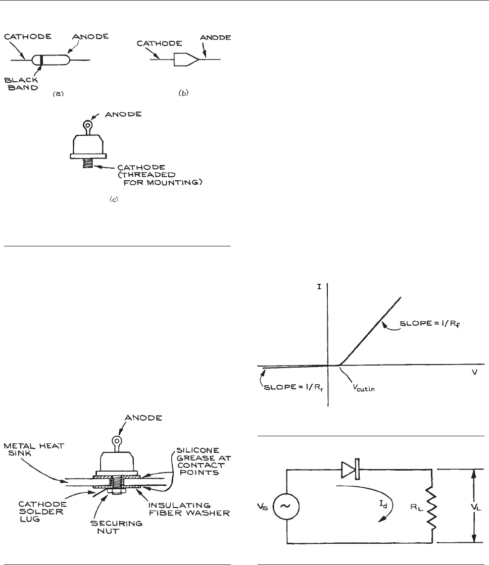
between the washers and heat sink. The mounting techni-
que is shown in Figure 6.35.
Because
the current through a diode is a nonlinear func-
tion of the voltage across it, the effective resistance
changes with diode voltage. This is shown in Figure
6.33, where the reciprocal of the slope of the curve passing
through
the origin and a point on the I–V characteristic
curve defines the static resistance at that point. The
dynamic resistance is the reciprocal of the slope of the
tangent to the curve at the point. The change in current
through a diode for small changes in voltage across it
requires knowledge of both static and dynamic resistance.
For the purposes of simplified circuit analysis, it is useful
to represent the I–V characteristic curve of a diode by a so-
called piecewise linear model. With this model, the for-
ward- and reverse-bias regions are represented by straight
lines with the transition occurring at the cutin voltage. The
piecewise linear curve is shown in Figure 6.36. The slope
of
the curve at voltages above V
cutin
is the reciprocal of the
average forward resistance. With this model it is a simple
matter to calculate the effect of the diode in a circuit, since
it behaves like a resistor in the forward-bias condition with
resistance R
f
, and in the reverse-bias condition it acts
essentially like an open circuit. A graphical representation
of this can be obtained by what is called load-line analysis.
Consider the circuit with an a.c. voltage source shown in
Figure 6.37 . The current through R
L
can be determined in
the following manner: given a value of V
s
, the voltage
across the diode, V
d
, and the current through it, I
d
, will be
determined by the intersection of the straight line with co-
ordinates (V
s
, 0) and (0, V
s
/R
L
), as in Figure 6.38. Different
Figure 6.34 Diode case configurations: (a) glass-
encapsulated signal diode; (b) plastic-encapsulated
medium-power diode; (c) high-power diode.
Figure 6.35 Power-diode mount provides electrical insula-
tion with good heat dissipation.
Figure 6.36 Linearized current–voltage characteristic of a
diode.
Figure 6.37 Circuit for load-line analysis of a diode.
ACTIVE COMPONENTS 405
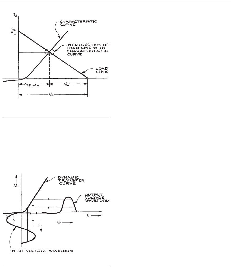
values of V
s
will give a family of parallel straight lines.
From the intersection points, one constructs a graph of V
L
as a function of V
s
. This dynamic curve, which is sho wn in
Figure 6.39, has much the same appearance as the original
s
tatic curve from which it is derived. If the input waveform
is drawn below the horizontal axis, the reflection of it on the
dynamic curve will give the output waveform as shown.
6.3.2 Transistors
Transistors are three-terminal devices. Any one of the
three terminals can be used as an input with a second
terminal as output and the third providing the common
connection between the input and output circuits.
Bipolar Junction Transistors (BJTs). These transis-
tors consist of an emitter, a base, and a collector. They are
designated npn or pnp, depending on the materials used for
the elements. As can be seen from Figure 6.40, a transistor is
tw
o back-to-back diodes with the base element in common.
The major current flow in a BJT transistor is from the emit-
ter to the collector across the base. Relatively little current
flows through the base lead. The arrow on the emitter shows
the direction of the current flow.
Some common BJT transistor case styles are shown in
Figure 6.41. To identify the leads of high frequency tran-
sistors,
manufacturers’ base diagrams should be consulted.
With plastic cases, there is a flat on one side of the case to
help identify the leads. Leads are sometimes identified by
letters, or are in the following order – emitter, base, col-
lector – starting at the flat or tab of sealed metal cans and
proceeding clockwise as viewed from the lead side of the
transistors. In power transistors, most of the power is dis-
sipated in the collector and the collector terminal is the one
with provision for attachment to a heat sink. Standard
transistor types have code designations beginning with
2N. Several manufacturers often make the same transis-
tors. Proprietary code designations are also used by man-
ufacturers to identify their products.
Since BJT transistors consist of two p-n junctions, a simple
ohmmeter test is a good way to verify that they are in working
condition once the transistor is isolated from the circuit. The
ohmmeter must provide at least 0.6 V, enough to forward-bias
a silicon p–n junction. The resistance between the emitter and
base should be low, of the order of a few hundred ohms or
less when the ohmmeter leads are attached so as to forward-
bias the junction. When the leads are reversed, the resistance
should be of the order of megohms. The same should be true
of the collector–base junction. The polarity of the ohmmeter
leads can be checked with a separate voltmeter.
In normal operation, the emitter–base junction of a tran-
sistor is forward-biased, while the base–collector junction is
reverse-biased. The three usual configurations, common
Figure 6.38 Graphical construction for determining
the dynamic transfer curve from the load line and the
static characteristic curve.
Figure 6.39 Graphical construction of output waveform
from input waveform and the dynamic transfer curve.
406 ELECTRONICS
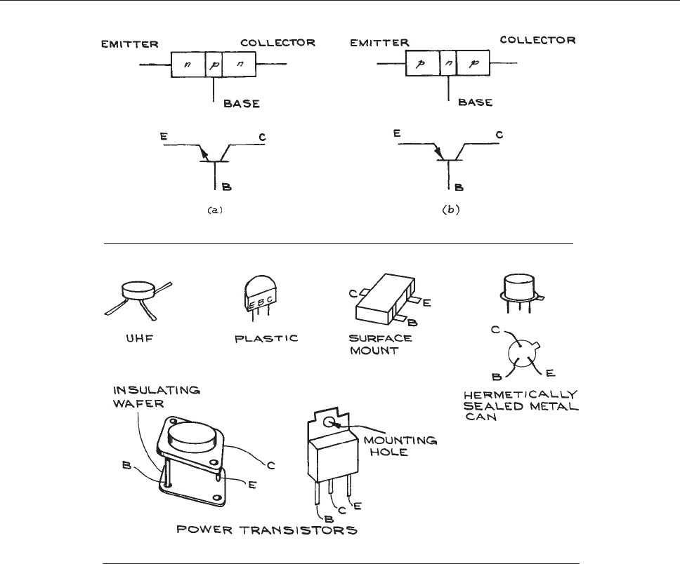
emitter (CE), common base (CB), and common collector
(CC), are shown schematically in Figure 6.42.TheI–
V
characteristics of each configuration consist of two sets of
curves, one for the input and the other for the output. The I–
V curves for a typical general-purpose transistor in the CE
configuration, for example, are shown in Figure 6.43. There
are a set of curves rather than a single one for the input and
output circuits because the two circuits interact with each
other. When measuring the I–V characteristics of either the
input or output circuit, the condition of the other circuit
must also be specified. Figure 6.44 shows a circuit for meas-
ur
ing the output characteristics of a CE configuration.
For a fixed series of I
B
values, set by adjusting V
BB
,the
current into the collector I
C
is measured as a function of V
CE
.
The variation in V
CE
is obtained by changing V
CC
. Transistor
operation can be understood in terms of the characteristic
curves. For a fixed value of I
B
, I
C
increases rapidly with V
CE
until a plateau is reached. I
C
increases thereafter much more
slowly with V
CE
. In the plateau region, the value of I
C
depends on I
B
and is almost independent of V
CE
.Thiscan
be made more quantitative by using load-line analysis. Two
points are sufficient to establish the load line on the output
curves – they are points corresponding to I
C
¼0 where V
CE
¼
V
CC
and to V
CE
¼ 0 where I
C
¼ V
CC
/R
L
. The output curves
Figure 6.40 Bipolar junction transistors (BJTs) and the corresponding symbols.
Figure 6.41 Transistor case styles.
ACTIVE COMPONENTS 407
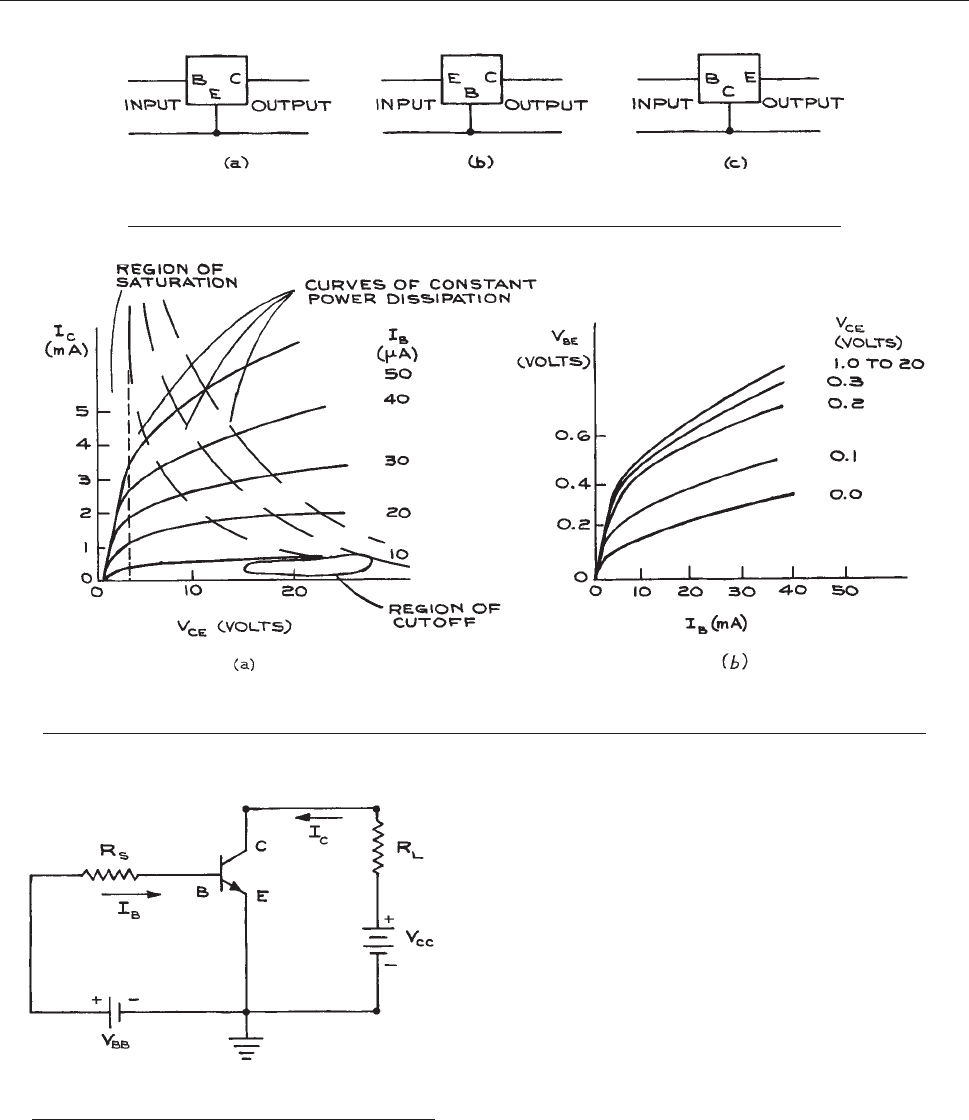
with a superimposed load line are shown in Figure 6.45.
The intersections of the load line with the characteristic
curves establish the operating voltages and currents. It is
possible to predict quantitatively how the current through
R
L
varies with input base current from these curves. For
linear operation, conditions are adjusted so that the tran-
sistor operates somewhere in the middle of the character-
istic output curves, where they are approximately spaced
equally and parallel for equal base-current increments.
Another way of analyzing transistor operation is by con-
structing an equiv alent circuit with passiv e elements and
sources. Such a circuit can then be analyzed by standard
methods. Because the equiv alent circuit contains only linear
Figure 6.42 (a) Common-emitter (CE), (b) common-base (CB), and (c) common-collector (CC)
configurations.
Figure 6.43 Current–voltage characteristics of a BJT transistor in the common-emitter (CE) configuration:
(a) output circuit, and (b) input circuit.
Figure 6.44 Biasing circuit for the BJT common-
emitter (CE) configuration.
408 ELECTRONICS
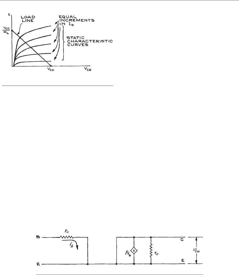
elements, it can represent the properties of the transistor only
within a small region of the characteristic curves about giv en
nominal v alues of the d.c., steady-state, or quiescent voltages
and currents. For this reason such a model is called a small-
signal model. A simplified low-frequency, small-signal cir-
cuit model of the BJT transistor in the CE configuration
treats the output circuit as a controlled current source with
i
c
¼ bi
b
in parallel with output resistance r
o
.Herei
b
is the
base current and b, the ratio of collector current to base
current, is the current gain, a constant. The input circuit
can be modeled as a forward-biased diode with r
p
the diode
effective resistance. The cutin voltage of the diode is
assumed to be constant and for this reason does not appear
in the small-signal model. This is shown in Figure 6.43(a).
It
is necessary to keep in mind that the linear circuit is a
good representation of the transistor only for small excur-
sions of the input and output voltages and currents about
specified quiescent d.c. values. The equivalent circuit does
not show the biasing network necessary to establish the qui-
escent operating point. Practical circuits using separate power
supplies for biasing voltages are shown in Figure 6.47.
The
output signal is developed across the load resistor
R
L
, while capacitors C
i
and C
o
isolate the a.c. input and
output signals from the d.c. biasing levels.
Transistor data sheets give the values of the b, the cur-
rent gain, and r
p
, the input resistance, for different operat-
ing points. The parameters for the CB and CC
configurations can be calculated from those of the CE with
standard formulae.
3
By applying the standard methods of
circuit analysis to the equivalent circuit, the current, volt-
age, and power gains can be calculated, as well as the input
and output impedances under small-signal conditions. The
general properties of the three configurations are given in
the graphs of Figure 6.48. Because the charge carriers in
the p-
and n-materials that make up the transistor cannot
respond instantaneously to changes in voltage across the
junctions, the simple three-parameter (r
p
, b,r
o
) model is
approximately valid only at low frequencies. The response
of the transistor at high frequencies can be very different,
and equivalent-circuit models exist for the high-frequency
response. In these models, the effective capacitances
between the base-emitter, base-collector, and collector-
emitter are represented by capacitors C
be
, C
bc
, and C
ce
shown in Figure. 6.49 .
A BJT can also be operated as a switch. If the emitter–
base junction of a transistor is strongly forward-biased
(0.8 V for silicon), the total current through the transistor
will be limited by the external resistance in the circuit and
the voltage between emitter and collector will be of the
order of 0.2 V. In this condition, the transistor is said to be
saturated or on and the base current necessary to sustain
the current flow from emitter to collector is I
C
/b
F
, where I
C
is the total current in the collector circuit and b
F
is the large
signal current gain. If the emitter–base junction is reverse-
biased, no base current will flow and no collector current
will flow. Under this condition, the transistor acts as an
Figure 6.45 Relation between the static characteristic
curves and the load line.
Figure 6.46 Small-signal model of a BJT.
ACTIVE COMPONENTS 409
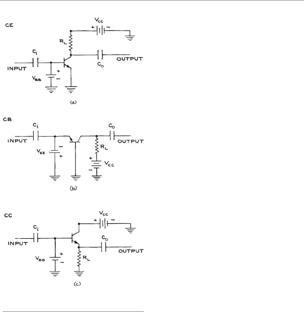
open circuit and is said to be cut off. In the saturated or the
cut-off condition, a transistor is similar to a closed or an
open switch. Transistor switches can operate at high fre-
quencies, unlike mechanical switches, but the saturated
resistance is never zero, and there is always at least a
0.2 V drop from the emitter to the collector.
The operating conditions for bipolar junction transistors
are summarized in Table 6.16. They determine whether a
transistor
is operating in the linear region (active), is satu-
rated,oriscut off. When reading the specifications for a
2N3904 transistor in Tables 6.16 and 6.17, the following
con
ventions are to be noted:
(1) Voltages between two terminals are specified by
either V or v with two or three subscripts. The first
two subscripts indicate the terminals between which
the voltage occurs, and the third subscript, when
present, indicates the condition of the third ter-
minal. Thus, V
CBO
indicates a d.c. voltage between
collector and base with the emitter open. Subscripts
with repeated letters indicate power-supply voltages.
For example, V
CC
is the power-supply voltage to the
collector, and V
BB
is the power-supply voltage to the
base.
(2) By convention, all currents are taken to be positive
when they flow into the leads of the transistor and
negative when they flow out of the leads.
(3) Currents are specified by I or i with a subscript indicating
the terminal inv olv ed. I
B
is therefore a d.c. base current.
Transistors are destroyed if their maximum power capa-
bilities are exceeded, or if, when reverse-biasing the junc-
tions, the maximum reverse voltages are exceeded,
resulting in electrical breakdown. The maximum power
dissipation depends on temperature, and a transistor fixed
to a heat sink can dissipate considerably more power than
one standing alone in free air. In pulse operation, the max-
imum steady-state power levels can be momentarily
exceeded without damage.
Field-Effect Transistors (FETs). The junction FET
or JFET is the simplest FET. It has three terminals – a
source, a gate, and a drain. An n-channel device is shown
in Figure 6.50. Current flow is from source to drain with the
ga
te re ve rse-bias ed with respect to the channel. Because of
this reverse bias, negligible current flo ws into the gate. The
I–V charac teristics of a small-signal JFET are sho wn in
Figure 6.51. From the curves it can be seen that there is a
reg
ion where the drain current decreases with increasing
Figure 6.47 Practical transistor circuits using separate
power supplies for biasing voltages: (a) common emitter;
(b) common base; (c) common collector.
410 ELECTRONICS
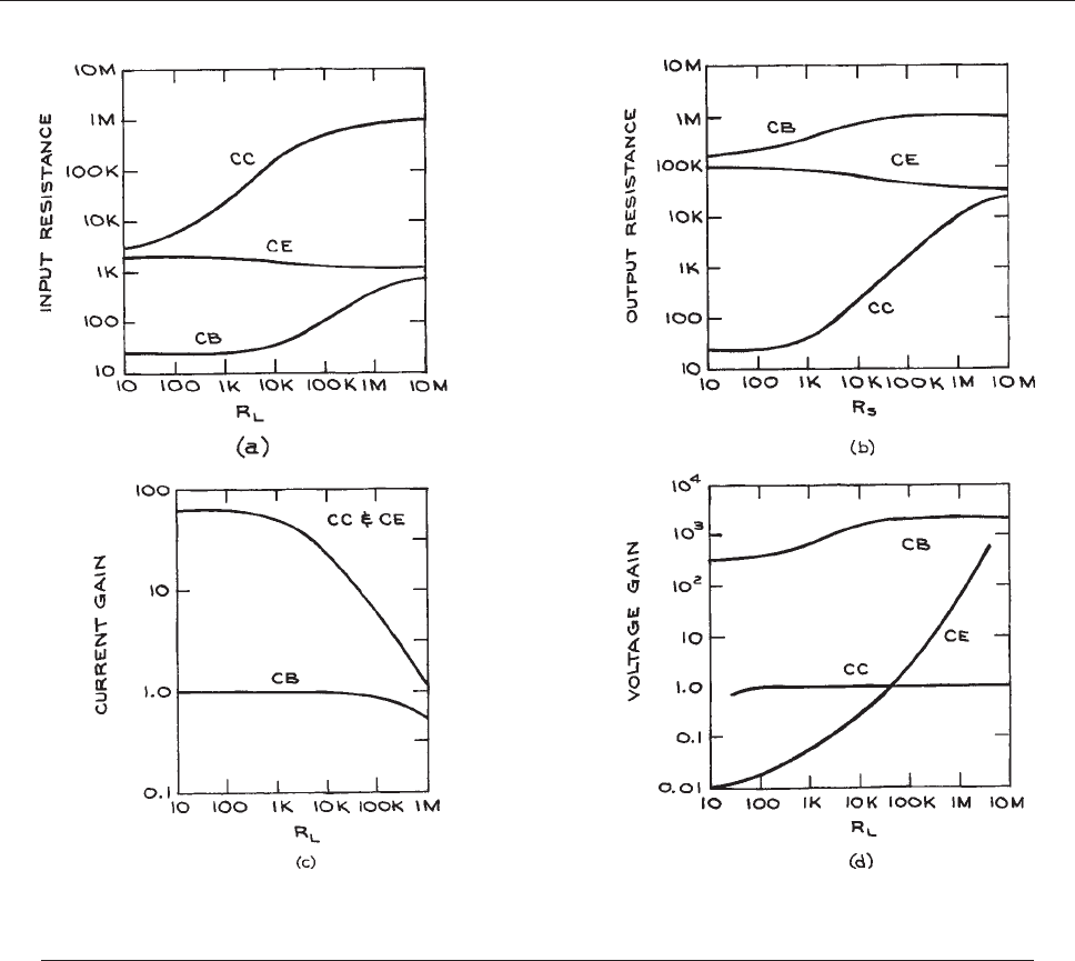
rev erse bias from the gate to source, independent of the drain-
source voltage. This is the region where the transistor can be
operated as an amplifier. About the region V
DS
¼ 0, I
D
increases linearly with V
DS
for fix ed V
GS
,withtheslope
equal to the reciprocal of the channel resistance R
channel
.
As V
GS
becomes more negative, R
channel
increases. Transistor
operation in this region is that of a voltage-controlled r esi stor.
The FET can also be used as a switch, with the advantage
of no offset voltage from source to drain and almost perfect
electrical isolation of the gate signal from the output circuit.
Disadvantages are rather high on resistances (of the order
of hundreds of ohms) and low off resistances. Also, switch-
ing times are greater than for BJTs.
The simple structure of FETs results in low noise. As a
consequence, FETs are often used as the active elements in
low-level signal amplifiers. Field-effect transistors with
gates insulated by an oxide layer from the conducting
channel are called MOSFETs (metal oxide-semiconductor
Figure 6.48 Variation of the properties of the CE, CB, and CC transistor configurations with various input parameters:
(a) input resistance as a function of load resistance; (b) output resistance as a function of source resistance; (c) current
gain as a function of load resistance; (d) voltage gain as a function of load resistance.
ACTIVE COMPONENTS 411
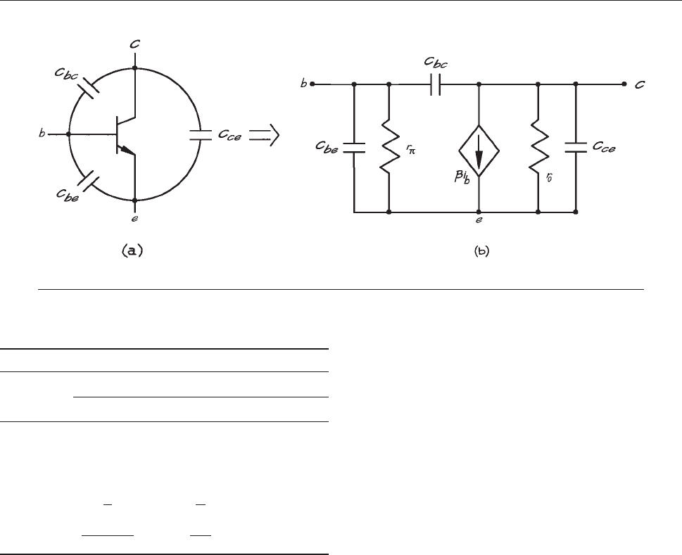
FETs). The oxide gate insulation effectively blocks any
d.c. gate current flow. The conducting channel in a MOS-
FET can be either p-doped (PMOS) or n-doped (NMOS).
Moreover PMOS and NMOS transistors can be of the
depletion mode or enhancement mode. For depletion-mode
transistors, the maximum drain current corresponds to
V
GS
¼ 0. For both PMOS and NMOS enhancement-mode
transistors, there is no drain current at V
GS
¼ 0. Only when
V
GS
reaches the threshold value V
T
, will drain current flow.
For NMOS enhancement V
T
is approximately þ2 V, for
PMOS enhancement V
T
is approximately 2 V. The con-
struction of PMOS and NMOS depletion-and enhance-
ment-mode transistors along with their schematic symbols
are shown in Figure 6.52. Typical characteristic output
curv
es are given in Figure 6.53.
D
epletion-mode MOSFETs are less common that
enhancement-mode devices because of their relatively low
transconductance (ratio of output current to input voltage).
Because of the higher mobility of electrons compared to
holes, NMOS transistors have properties that are superior
to PMOS transistors. The most common application of
PMOS transistors is in CMOS logic circuits (see Section
6.
6.10). Low power consumption, ease of fabrication, and
hi
gh packing densities have made MOSFETs extremely
common in large-scale (LSI) and very large-scale (VLSI)
integrated circuits.
Because of the gate insulation, static charge can accu-
mulate on the gate and voltage can build to levels sufficient
to punch through the insulation. To avoid this, some MOS-
FET gates are protected with reverse-biased Zener diodes.
MOSFET devices are normally packaged in conducting
foam or with metal protecting rings that are removed just
prior to insertion into the circuit.
For switching high currents, the bipolar junction tran-
sistor was the device of choice until the development of the
power MOSFET and the insulated gate bipolar transistor
(IGBT). Because the BJT is current controlled and the
MOSFET is voltage controlled, the MOSFET has a num-
ber of significant advantages at moderately high voltages
Figure 6.49 BJT showing: (a) Junction capacitances and (b) small-signal model with junction capacitances.
Table 6.16 2N3904 Transistor parameters
Condition of Transistor
Parameter Active Saturated Cut-Off
V
BE
0.6 V 0.8 V < 0.0 V
V
BC
510 V
(reverse bias)
0.6 V
(forward bias)
V
CC
(reverse bias)
V
EC
510 V 0.2 V V
CC
I
B
(i
b
)
i
c
b
I
c
b
’ 0
I
C
V
CC
V
CE
R
L
V
CC
R
L
’ 0
412 ELECTRONICS
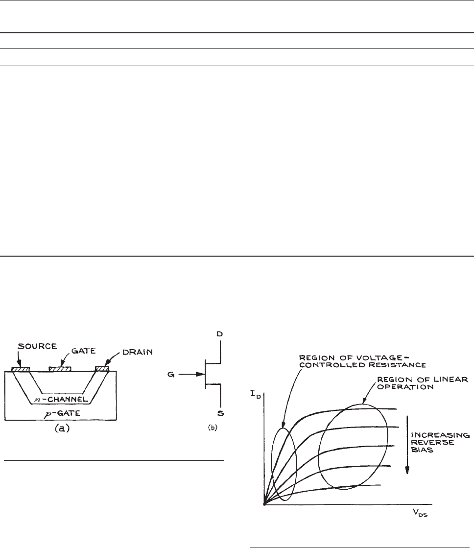
and currents and especially at high switching speeds. The
current-carrying capacity of a small-signal MOSFET is
limited by the size of the conducting channel. One way
to increase current capacity is with a short and wide chan-
nel that has the form of a trench or groove. This is shown
in Figure 6.54 for an enhancement n-channel
power
Table 6.17 Properties of the 2N3904 N–P–N silicon transistor
Condition Parameter Value Conditions
Absolute Maximum Ratings V
CBO
60 V I
C
¼ 10 lA, I
E
¼ 0mA
25 °C in Free Air V
CEO
40 V I
C
¼ 1 mA, I
B
¼ 0 lA
I
C
(continuous) ¼ 200 mA V
EBO
6V I
E
¼ 10 lA, I
C
¼ 0mA
Maximum Power Dissipation ¼ 310 mW
‘‘On’’ Characteristics b
F
40 V
CE
¼ 1V,I
C
¼ 100 lA
70 V
CE
¼ 1V,I
C
¼ 1mA
V
BE
a
0.65 to 0.85 V I
B
¼ 1 mA, I
C
¼ 10 mA
0.95 V I
B
¼ 5 mA, I
C
¼ 50 mA
V
CE
a
0.2 I
B
¼ 1 mA, I
C
¼ 10 mA
0.3 I
B
¼ 5 mA, I
C
¼ 50 mA
Small Signal Characteristics r
p
1kX to 10 kX
b 100–400 V
CE
¼ 10 V, I
C
¼ 1 mA,
r
o
25 kX to 1 MX
f
T
b
300 MHz V
CE
¼ 20 V, I
C
¼ 10 mA
C
obo
c
4pF V
CB
¼ 5V,I
E
¼ 0mA
C
ibo
d
8pF V
EB
¼ 0.5 V, I
C
¼ 0mA
a
Saturation.
b
Frequency for b ¼ 1.
c
Common-base open-circuit output capacitance.
d
Common-base open-circuit input capacitance.
Figure 6.50 N-channel junction field-effect transistor
(JFET): (a) Construction; (b) Symbol.
Figure 6.51 Current–voltage characteristics of a
small-signal, junction-field-effect transistor (JFET).
ACTIVE COMPONENTS 413
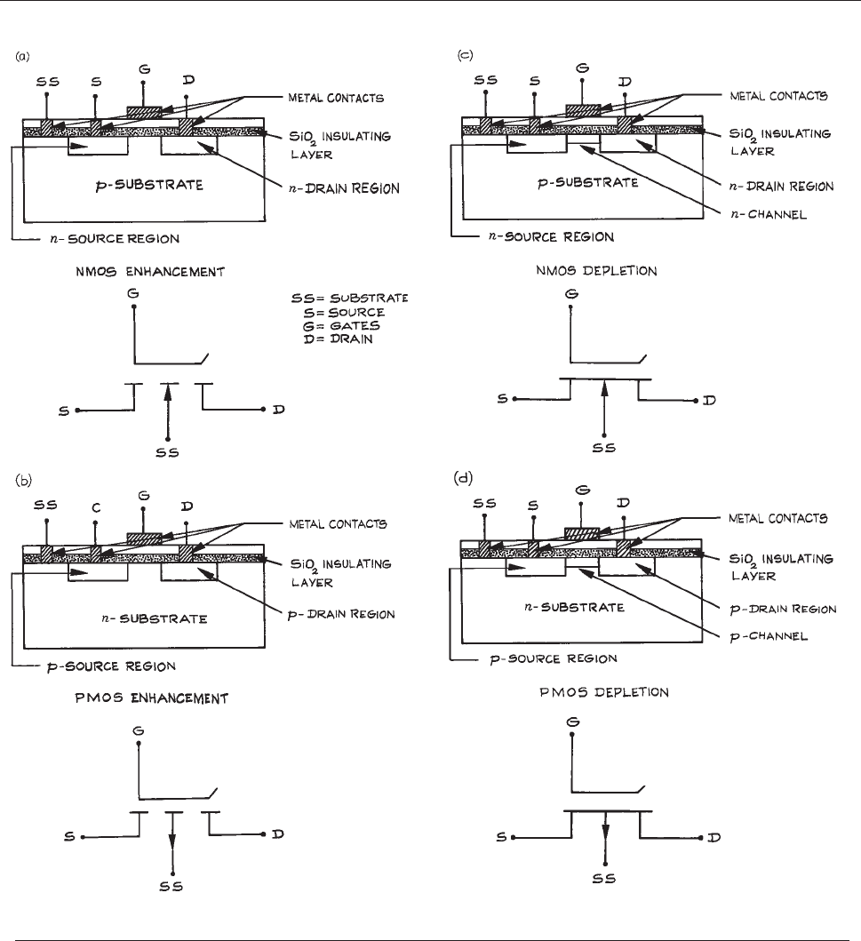
Figure 6.52 MOSFET structures and schematic diagrams. (a) NMOS enhancement; (b) PMOS enhancement; (c) NMOS
depletion; (d) PMOS depletion.
414 ELECTRONICS
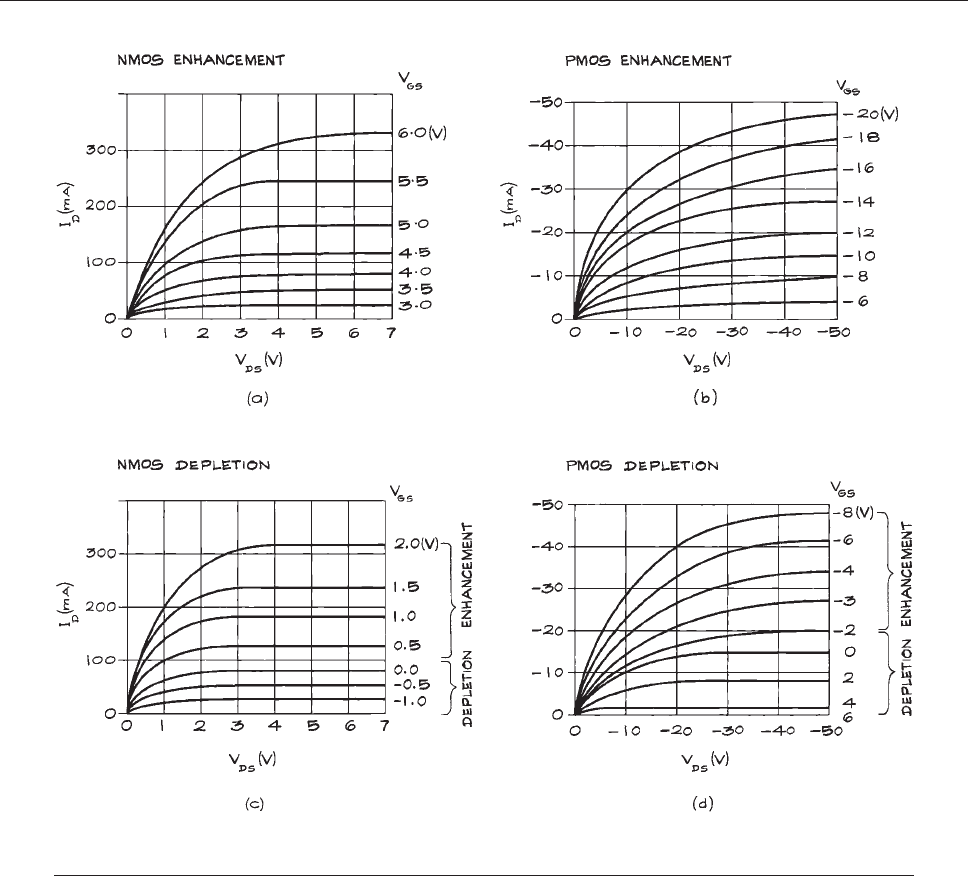
MOSFET. The materials are labeled p, n
+
, and n
indicat-
ing p-doped material, lightly n-doped material, and heavily
n-doped material. With the drain biased positive with
respect to the source and the gate at the source potential,
no current flows between drain and source because the p–n
junctions are reverse biased. As the potential of the gate is
increased with respect to the source, an n-channel is
formed around the gate, resulting in a conduction path from
source to drain. The I–V static characteristics of a typical
n-channel enhancement power MOSFET, the VN66AFD, is
shown in Figure 6.55. The main characteristics to note are:
(1)
Drain current is essentially zero for V
GS
less than 2 V.
This is the threshold voltage and varies from 0.5 to
2.5 V for power MOSFETs.
(2) Between V
DS
¼ 2 V and V
DS
¼ 4V, I
D
is a nonlinear
function of V
GS
, increasing quadratically with V
GS
.For
V
GS
greater than 4 V, I
D
is a linear function of V
GS
.
Figure 6.53 MOSFET output IV characteristics: (a) NMOS enhancement; (b) PMOS enhancement; (c) NMOS
depletion; (d) PMOS depletion.
ACTIVE COMPONENTS 415
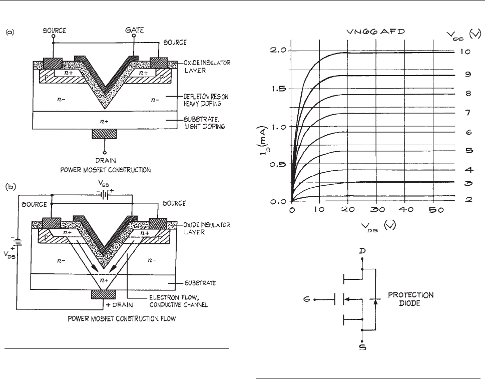
(3) I
D
depends almost entirely on V
GS
and is nearly inde-
pendent of V
DS
.
Because the gate is insulated by an oxide layer from the
underlying p and n materials, there is no current flow into
the gate under steady-state conditions. The input impe-
dance is essentially infinite. However, because the gate
acts as one plate of a capacitor, with the oxide insulating
layer as the dielectric, current can flow into the gate when
the voltage on the gate is changed. Typical gate capacitan-
ces are in the tens of picofarads. As a result, switching
times of nanoseconds are possible when the gate drive
voltage is derived from a low-impedance source.
The pow er MOSFET is an ideal voltage-controlled switch.
For the VN66AFD, the drain to source resistance, R
DS
,varies
from 2 X at V
GS
¼ 4Vand I
D
¼ 0.1 A to less than 1 X at
V
GS
¼ 10 V and I
D
¼ 0.1 A. For V
GS
¼ 2V, R
DS
is of the
order of megohms. Power MOSFETs can be switched with
TTL or CMOS gates. Sample interface circuits using the
VN66AFD are shown in Figure 6.56(a) and (b). W ith 5 V
on
the gate of the MOSFET, the saturation drain current is
0.8 A. Higher drain currents can be achiev ed by increasing
the MOSFET gate voltage.
While power MOSFETs are mostly used in switching
applications, they can also be used as power amplifiers by
biasing them into the linear portion of the characteristic
curve. This is shown in Figure 6.56(c). With this arrange-
ment
the quiescent drain current is 0.675 A with V
GS
¼
8.6 V. An input voltage swing of 61 V results in a change
of current of 60.17 A about the quiescent value. While
Figure 6.54 Power MOSFET: (a) Construction; (b) Current
flow.
Figure 6.55 VN66AFD power MOSFET output IV
characteristics and schematic diagram.
416 ELECTRONICS
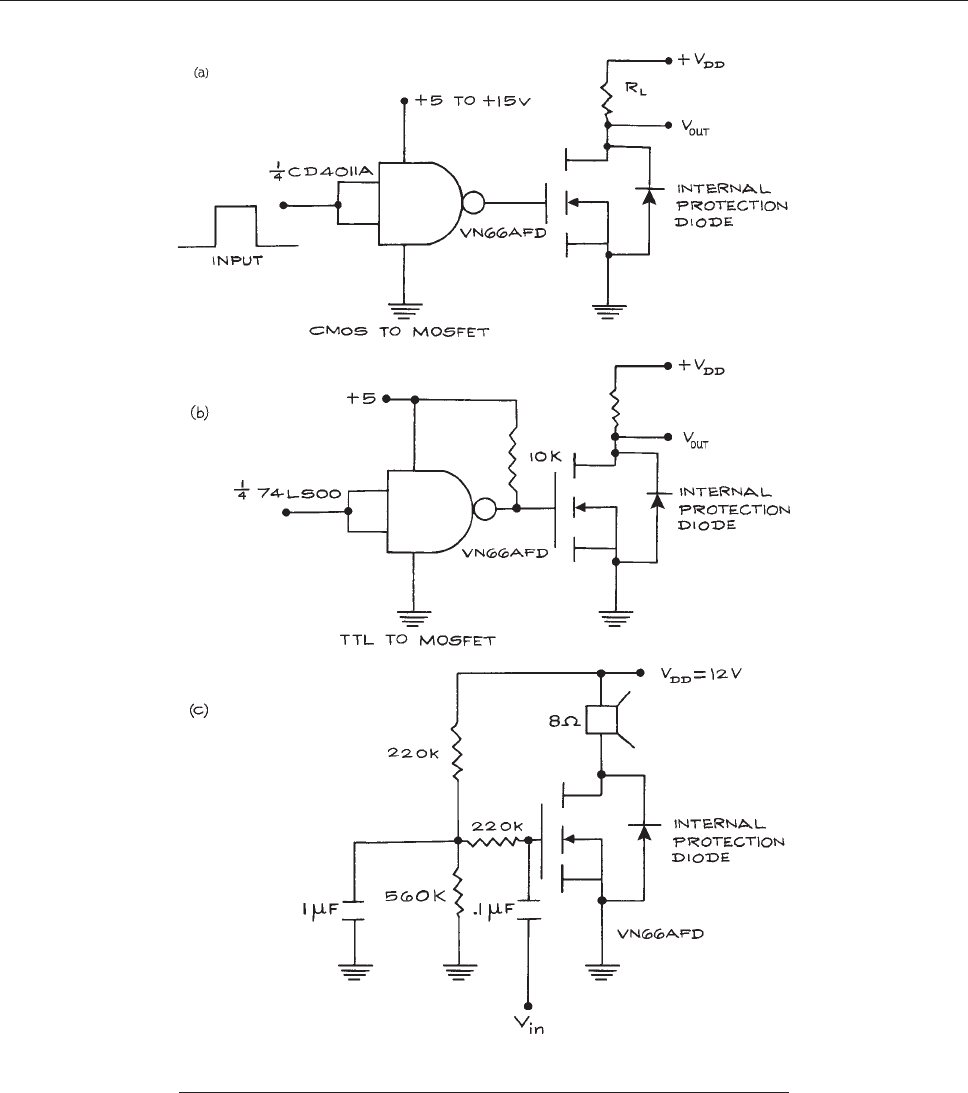
Figure 6.56 Power MOSFET circuits: (a) CMOS to MOSFET; (b) TTL to MOSFET;
(c) MOSFET power amplifier.
ACTIVE COMPONENTS 417
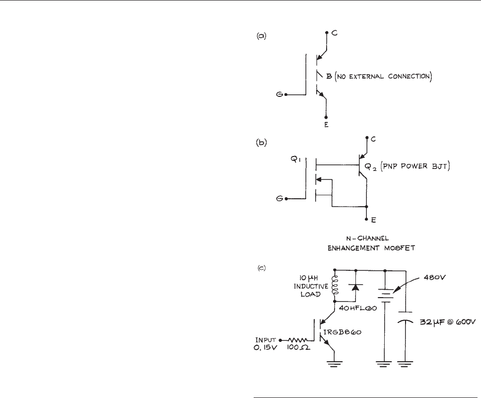
inefficient, the circuit is simple and has less than 1% har-
monic distortion at 1 W.
Commercial applications for power MOSFETs are in
switch mode power supplies, motor controllers, lamp
drivers, and automotive ignition systems. While trench
and V power MOSFETs are common, there are other
MOSFET configurations based on laterally diffused
(LDMOS) geometries and pa rallel arra ys of MOSFETs
(HEXFETs). An important property of e nhancement
MOSFETs that allows them to be connected in parallel
is the drain-current negative-temperature coefficient. This
means that as the temperature of the device increases, the
drain current will decrease. This is a consequence of
majority carrier conduction in the drain-source channel.
By contrast, the collector-current temperature coefficient
in BJTs is positive; collector cur rent increases with tem-
perature, leading to the possibility of thermal runaway, in
which increasing temperature leads to increasing collec-
tor current that increases power dissipation and higher
temperatures, etc.
Power MOSFETS can operate at frequencies well in
excess of 100 kHz. While maximum voltages as high as
1000 V are available, most power MOSFETs are designed
for operation below 300 V. Current handling capabilities
extend to 100 A.
The IGBT i s a device t hat combines the high input
impedance of a power MOSFET with the high current
capabilities of a power BJT. The schematic symbol for
aIGBTisgiveninFigure 6.57(a) along with a simplified
eq
uivalent circuit in Figure 6.57(b). The device is ‘‘on’’
w
henthebase(B)ofthep-n-p output transistor is neg-
ative with respect to the collector (C) by 0.6 to 0.8 V. The
total voltage drop from C to E is equal to the voltage drop
across the CB diode plus the drop acr os s t he input MOS-
FET. This latter voltage drop is a functi on of the gate-to -
source voltage, V
GS
. The use of IGBTs is restricted to
switching applicat ions. In Table 6.18 the switching char-
a
cteristics of power M OSFETS, IGBTs, an d power BJTs
are compared.
The IGBT offers clear advantages over power MOS-
FETs at voltages above 300 V and at high currents and
speeds from 5 to 50 kHz. They are to b e preferred in
high-power applications with voltages greater than
1000 V provided the frequency requirements are less
than 20 kHz, the duty cycle is low, and variations in
load and line are small. A representative IGBT is the
IRGB860. It is available in TO-220AB, TO262, and
D
2
Pak packages. The maximum collector-to-emitter
voltage is 600 V and the maximum continuous collector
current is 28 A at 25 °C, falling to 19 A at 100 °C. The
maximum value of V
GE
is 620 V. Exceeding this limit
subjects the device to permanent damage through
destruction of the insulating layer between gate and sub-
strate. When ‘‘on’’ (V
GE
¼ 15 V and I
C
¼ 8A),V
CE
is
approximately 2 V. Switching rise times are 20 to 30 ns
and fall times are 30 to 40 ns. Maximum power
Figure 6.57 IGBT: (a) schematic diagram; (b) internal
connections; (c) inductive load switching at high voltage.
418 ELECTRONICS
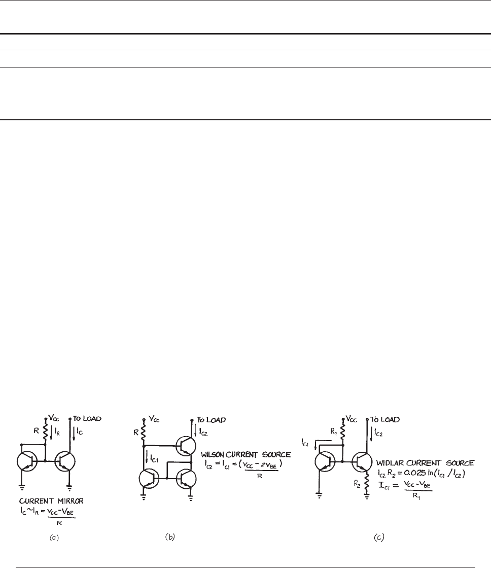
dissipation is 167 W a t 25 °C and 83 W at 100 °C. It is
worthnotingthatV
CE
decreases with temperature so that
there is the possibility of thermal runaway in high-power
applications. This is not the case for power
MOSFETs. A circuit for switching an inductive load with
an IRGB860 is shown in Fig ure 6.57(c). T he diode sup-
presses
inductive voltage transients associated with
the switching of currents through the inductor. This pro-
tects the IGBT and results in cleaner switching wave-
forms.
Active Loads and Current Sources. Both BJT a nd
FET transistors can be used as resistors with static resis-
tances of kilohms and dy namic resista nces of te ns and
even hundreds of kilohms. Ac tive loads ar e commonly
used in integrated circuits w here resistors are difficult
to fabricate. The high dynamic resistance (dv/di)ofBJTs
and FETs in their active region is also used for high out-
put-impedance current-source circ ui ts. Examples of BJT
current-source circuits are given in Figure 6.58.An
NMOS
depletion-mode transist or can also be converted
to a resistor by connecting the drain to the gate. The
nonlinear I–V character istics of this configuration ca n
be found from t he output characteri stics of the transistor
with V
GS
¼ V
DS
.
6.3.3 Silicon-Controlled Rectifiers
The silicon -controlled rectifier, SCR, is a switching
device with only two states – on and off.Intheon state,
the SCR has a low resistance, and some models are capa-
ble of passing over 100 A. In the off s tate, the resistance is
in the megohm range. The SCR has three terminals: an
anode,acathode,andagate. The transition from off to on
Table 6.18 Comparison of the properties of power MOSFET, IGBT and power BJT transistors
Input/Output Power MOSFET IGBT Power BJT
Input Power Very low Very low Moderate to high
Output Current High at low voltages,
low at high voltages
Very high, almost independent
of switching speed
Moderate, strong function
of switching speed
Switching Losses Very low Low to moderate Moderate to high
Figure 6.58 Current sources.
ACTIVE COMPONENTS 419
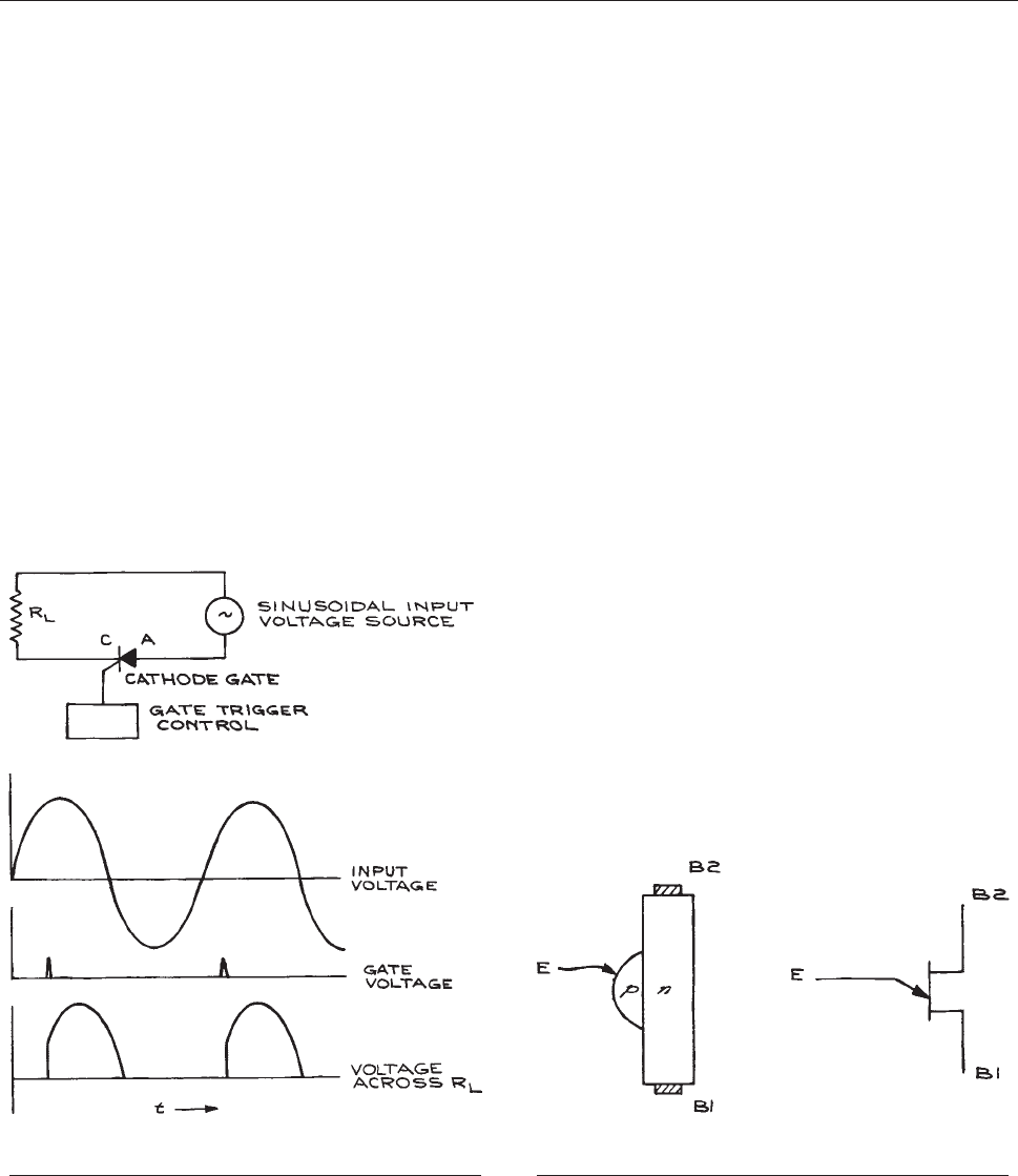
occur s when the voltage on the anode is positive wi th
respect to the cathode and a pulse of the corr ect polarity
and magnitude is applied to the gate. Once the SCR is on,
the gate loses all control over the functioning of the
device. The only way to turn it off is to reduce the
anode–cathode voltage to zero. If a sinusoidal voltage is
applied to the SCR anode, the device will be turned off
once each half cycle. By controlling the point in each
positive half cycle when the trigger pulse is applied, the
average current through the SCR can be varied over wide
limits (see Figure 6.59). This way of regulating the power
to
a load is very efficient because very littl e power is
dissipated in the SCR. When the SCR is off,thereisno
current through it and the power dissipation is zero. When
the cur rent through the SCR is at a maximum, the voltage
across it is low, result ing in low power dissipation. Bilat-
eral triggering can be accomplished with a bilateral switch
or triac. A common application of this kind of power
control is the incandescent light dimmer. High-power
switching devices like the SCR and triac produce radio-
frequency in terference (rfi) during switching when there is
a voltage across them. Zero crossing switch ing avoids rfi
by timing the switching to tho se instants when there is no
voltage across the device. Silicon-controlled switches
(SCSs) a re similar to SCRs, but have the advantage of
being able to be turned off with a pulse.
6.3.4 Unijunction Transistors
The unijunction transistor (UJT) is a single bar of n-mate-
rial to the middle of which p-material is attached, forming
a p–n junction. This is shown schematically in Figure 6.60.
The
two ends of the bar are bases 1 and 2 (B1 and B2),
while the p-material is the emitter (E). When B2 is made
positive with respect to B1, there will be a potential gra-
dient along the bar and the potential at the point of attach-
ment of the emitter will be a fixed fraction of the potential
across the bar. As long as the emitter is less positive than
the bar at its point of attachment, the emitter junction will
be reverse-biased and no current will flow through it.
When the emitter potential is increased sufficiently to
forward-bias the junction, current will flow in the E–B1
circuit and V
EB1
will fall. This is shown in the character-
istic curve (see Figure 6.61). A common application of
the
UJT is in relaxation oscillators where a capacitor is
charged through a resistor to the peak potential of the
UJT and then discharged. The UJT is also used in trigger
Figure 6.59 Current regulation with a silicon-controlled
rectifier (SCR).
Figure 6.60 Unijunction transistor (UJT) and the
corresponding schematic symbol.
420 ELECTRONICS
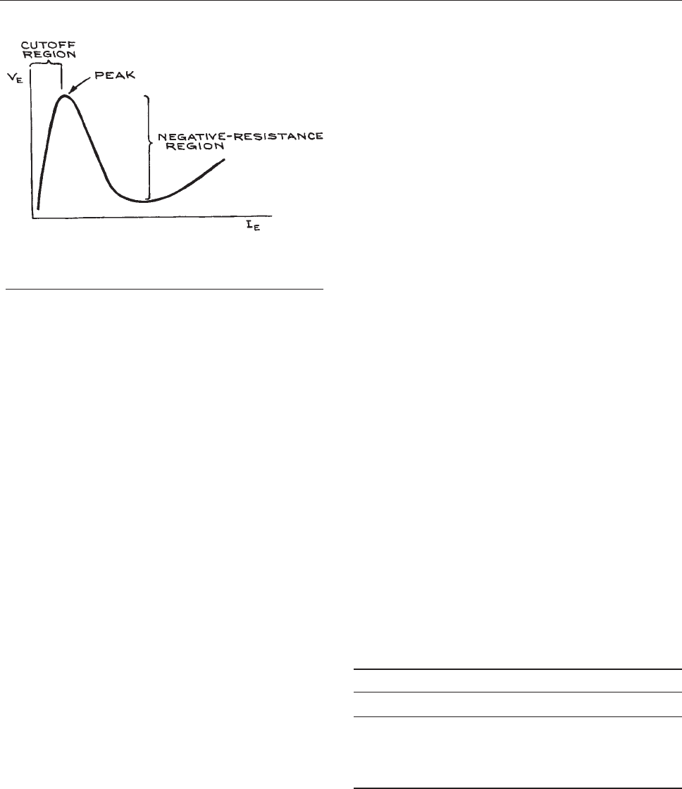
circuits, pulse generators, and frequency dividers. The sta-
ble peak voltage, which is a fixed fraction of the interbase
voltage, and high pulse-current capability make the UJT
very useful for SCR control circuits.
6.3.5 Thyratrons
For fast switching of high currents at high voltages, gas-
filled tubes called thyratrons are used. They are analogs
of SCRs and consist of a heated cathode, an anode, and a
grid sealed into a glass, gas-filled envelope. An arc can
be struck between the cathode and anod e, with the ini-
tiation of the arc controlled by the potential on the grid.
The grid is usually a cylindrical structure surrounding the
anode and cathode from which a baffle or series of baffles
with small holes extends between anode and cathode.
Since the anode and cathode are almos t completely
shielded from each other, only a small grid potential is
needed to overcome the field at the cathode resulting
from the large anode potential. Once the arc has been
initiated, the grid loses control over the arc. Grid control
is re-established only when the anode potential falls
below the level nece ssary to sustain the a rc. Deute-
rium-filled thy ratrons can switch hundreds of a mperes
at tens of kilovolts in microseconds or less and are com-
monly used in the high-voltage discharge sources of
lasers. SCRs are often used to supply the trigger pulse
to the grid of the thyratron.
6.4 AMPLIFIERS AND PULSE
ELECTRONICS
6.4.1 Definition of Terms
In laboratory applications, amplifiers are used to transform
low-le v el signals to levels suffi cient for observation and
recording, or for operation of electronic or electromechani-
cal devices. When choosing an amplifier for a given task,
there are a number of considerations that require the defini-
tion and explanation of several special terms. The goal is to
provide information for the experimentalist who must make
decisions regarding the use and specifications of amplifiers.
Amplifiers can be classified in a number of ways, among
them the following:
(1) By input and output variables
(2) By frequency domain
(3) By power levels.
Each of these classifications will be treated in turn, and
any given amplifier will have its place somewhere within
each of the classifications. The two most common electri-
cal input and output variables are current and voltage.
There are therefore four different possible types of ampli-
fier, corresponding to the two input-variable possibilities
and the two output-variable possibilities. These are listed
in Table 6.19. The gain of
an amplifier is the ratio of the
output variable to the input variable. This is the equivalent
of the transfer function for the passive circuits already
considered. For voltage and current amplifiers, the gain
is unitless. For the transconductance and transresistance
amplifiers, however, their gains have units of siemens
(ohm
1
or sometimes mho) and ohm, respectively.
There are also amplifiers for which the input variable is
the time integral of the current or the charge. Such charge-
sensitive amplifiers have a voltage as an output, and the
Figure 6.61 Current–voltage characteristic curve for a
unijunction transistor showing the region of negative
resistance.
Table 6.19 Types of amplifier
Input Variable Output Variable Amplifier Type
Voltage Voltage Voltage
Voltage Current Transconductance
Current Voltage Transresistance
Current Current Current
AMPLIFIERS AND PULSE ELECTRONICS 421

gain is expressed in volts per coulomb or inverse farads.
Amplifiers with the time derivative of current as an input
variable are also possible.
The amplifiers in Table 6.19 have very different input
and
output properties. If the input is a current, the amplifier
should have a low input impedance so as to affect the
source as little as possible. On the other hand, if the input
is a voltage the input impedance should be as large as
possible to avoid drawing current from the source and
changing the source output voltage. The opposite consid-
erations apply to the outputs of the amplifiers. If the output
is a current, it is desirable that the output be close to that of
an ideal current source – that is, a very high output impe-
dance. If the output is a voltage, the output impedance
should be low to approximate an ideal voltage source as
closely as possible. These considerations of input and
output impedance (see Table 6.20) are of fundamental
import
ance when matching an amplifier to a detector or
transducer at the input and a load at the output. If the input
device is a current source, one should generally choose a
current, transresistance, or charge-sensitive amplifier; if the
input device is a voltage source, a voltage or transconduc-
tance amplifier is required. This assumes that amplification
with minimum loading of the input circuit is desired. When
efficient power transfer is desired, the impedances of the
source and load should match the input and output impe-
dances of the amplifier as closely as possible.
Amplifiers can be divided into groups according to the
frequency domain in which they are designed to operate
(see Table 6.21). Consider the Bode plots of gain and phase
shift
shown in Figure 6.62 for a capacitance-coupled
in
verting (output 180° out of phase with input) amplifier.
The curves can be understood qualitatively in the follow-
ing ways – at low frequencies the coupling capacitors
(capacitors in series with input and output to block d.c.
levels) reduce the low-frequency gain just like a high-pass
filter. At high frequencies the reduced gain of the active
devices (transistors) has the effect of shunt capacitances
across both the input and output circuits of the amplifier,
resulting in properties similar to that of a low-pass filter.
The frequency difference between the corner frequencies
(3 dB points of the gain curve) is the bandwidth of the
amplifier. Because the low corner frequency is usually
orders of magnitude smaller than the high corner frequency
(except in the case of tuned amplifiers that operate over a
very small frequency range), the bandwidth can be consid-
ered equal to the upper corner frequency. An often-used
figure of merit for amplifiers is the gain-bandwidth product
(GBWP), which is the midband gain times the bandwidth.
By this criterion, a low-gain, wide-bandwidth amplifier is
equivalent to a high-gain, narrow-bandwidth amplifier.
If it is possible for the output of an amplifier to be
coupled back to the input (ca pacitan ce coupling is
always present to some degree because of stray capaci-
tances)insuchawayastobeinphasewiththesignalat
the i nput, a positive feedback or regenerative situat ion
will occur, giving rise to oscill ations and unstable behav-
ior. This is the origin of the familiar squawking and
whistling that occurs in public address systems when
the output from the loudspeakers finds its way back to
the microphone. The stability of an amplifier against
such oscillations is expressed in terms of gain and phase
margins. If the value of the gain of an amplifier (in dB) is
negative at frequencies for which the phase of the output
is equal to that of the inpu t, oscillations cannot occur.
Correspondingly, if the output is out of phase with the
Table 6.20 Amplifier impedances
Amplifier Type Input Impedance Output Impendance
Voltage High Low
Transconductance High High
Transresistance Low Low
Current Low High
Charge-sensitive Low Low
Table 6.21 Amplifier frequency ranges
Amplifier Type Frequency Range
d.c. 0 to 10 Hz
Audio 10 Hz to 10 kHz
r.f. 100 kHz to 1MHz
Video 30 to 1000 MHz
VHF 30 to 300 MHz
UHF 300 to 1000 MHz
Microwave 1000 MHz to 50 GHz
422 ELECTRONICS

input at all frequencies for which the gain is greater than
unity, oscillations cannot occur. The amount of negative
gain at zero phase is the gain margin; the phase differ-
ence a t 0 dB gain is the phase margin (see Figure 6.63).
The
larger these margins, the more stable the amplifier.
Wide-band video amplifiers are particularly susceptible
to unstable behavior because even small stray capacitan-
ces are sufficient to provide low-impedance paths from
the output to the input for high frequencies. Because of
the large power consumption in the pos itive feedba ck
(regenerative) mode, prolonged unstable operation of
an amplifier can destroy it. This is especially true in
the case of fast-pulse amplifiers, which must have a very
large bandwidth in order to a ccurately amplify pulses
with short rise times. Compensation by the addition of
poles and zeros t o the transfer function can remedy this at
the expense of reduced b andwidth.
In classifying amplifiers by power rating, the distinctions
are rather arbitrary. Generally, preamplifiers are designed to
operate with input voltage levels of millivolts and less, input
currents of microamperes and less, and input charge of
picocoulombs and less. Gain is not so important in pream-
plifiers as is amplifier noise, which limits ultimate sensitiv-
ity. In some applications, a unit-gain preamplifier is used as
an impedance-matching device. Power amplifiers are
designed to furnish anywhere from a few to several hundred
watts to a matched load. Audio amplifiers are examples.
Intermediate between preamplifiers and power amplifiers
are amplifiers that operate with input signal levels from
preamplifier outputs and produce outputs from a few to
several hundred milliwatts. Gains of such amplifiers are
high, and noise considerations are much less important than
overload recovery. Frequency- and gain-compensating cir-
cuits are often incorporated in such amplifiers.
Figure 6.62 Bode plots for a capacitance-coupled inverting amplifier.
AMPLIFIERS AND PULSE ELECTRONICS 423
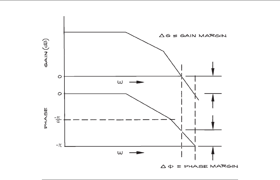
It has been assumed thus far that the output of an
amplifier is a linear function of the input at any fre-
quency. Because the active elements (transistors) in
solid-state amplifiers have nonlinear characteristics, it
follows that amplifiers can only operate in a linear way
within a limited range of input conditions. For all ampli-
fiers, there is an input signal level beyond which the out-
put signal is severely distorted. Clipping of the output
waveform is an obvious form of distortion. Less obvious
distortions can be quantified by a Fourier analysis of the
output waveform for a sinusoidal input. The distortion in
the output can be described in terms of the coefficients of
the harmonics. This harmonic distortion is important in
critical audio-amplifier applications, but not generally in
the laboratory.
The properties of solid-state amplifiers may also be tem-
perature-dependent, and such factors as gain and distor-
tion, though acceptable at room temperature, may become
unacceptable at high or low temperatures.
6.4.2 General Transistor-Amplifier
Operating Principles
The active elements in solid-st ate amplifiers can be n-p-n
or p- n- p bipolar junction transistors or field-effect tran-
sistors. Field-effect transistors can be n-channel or
p-channel and can be operated in the depletion or the
enhancement mode. They can have gate structures in
direct contact with the conducting channel (JFETs) or
gates that are insulated from the c on duct ing channel by
an oxide layer (MOSFETs).
To use an inherently nonlinear transistor to make a
linear amplifier requires ingenuity. Standard methods
involve operating the transistors over a limited range of
voltage and current where their nonlinear characteristics
can be approxim ated by linear functions, using comp en-
sating circuits to c ancel the nonlinearities with devices
that have opposite characteristics, o r applying negative
feedb ack.
Figure 6.63 Gain and phase margins.
424 ELECTRONICS

Transistors must be properly biased if they are to work
correctly. This means supplying, from external sources
such as batteries or d.c. power supply circuits, the correct
potential differences across the terminals and the correct
currents into them. Even in the absence of an external
signal, transistors dissipate power. The values of the d.c.
bias (or quiescent) voltages and currents define the operat-
ing point of the transistor. Signals from an outside source
or previous stage are then superimposed on the quiescent
values. As long as the signal does not represent too large a
deviation from these values, the transistor will operate
linearly. If the external signal is sufficiently large, however,
it can cut off the transistor (that is, reduce all the currents
through it to zero) or saturate it (that is, cause the transistor
to act as a short circuit).
Since the bias voltages and currents are d.c. and the
signal voltages and currents are a.c., it is possible to sep-
arate them. Capacitors or transformers can be used to cou-
ple a.c. signals without disturbing the quiescent d.c. values.
When capacitance coupling is used, the capacitors are
called blocking capacitors because they block d.c. voltages
and currents. Reasonably sized blocking capacitors usually
limit the low-frequency response of amplifiers to > 1 Hz
(capacitor lead inductance and stray shunt capacitances to
ground can also limit the high-frequency response). In
many applications, the poor transient response of the
high-pass circuits formed by the blocking capacitors can-
not be tolerated. Direct-coupled amplifiers – where the
bias levels of each transistor stage are designed to be com-
patible with the preceding and succeeding stages – provide
high gain to 0 Hz. Because of the need to match active
components and resistor ratios very precisely, such ampli-
fiers are often integrated-circuit (IC) amplifiers, where all
the elements of the circuit are manufactured simultane-
ously on a single chip. Direct-coupled designs are, in fact,
particularly suited to the IC manufacturing process, which
favors the production of transistors and diodes, but requires
quite special techniques for the production of resistors and
capacitors. Chopping is another method of achieving good
low-frequency response in amplifiers. With this method,
the input signal is chopped at a frequency much higher
than the highest characteristic frequency of the input sig-
nal. The resulting a.c. signal can be amplified by conven-
tional a.c.-coupled amplifier stages. Rectification of the
output of the final stage restores the input waveform. The
advantages of chopper over direct-coupled amplifiers are
lower uncompensated input currents and voltages, and
comparative freedom from drifts with temperature. These
advantages have been largely offset by IC direct-coupled
amplifier designs with FET input stages.
Amplifier properties and specifications are best under-
stood by considering as an example the general-purpose
741 IC operational amplifier. The name operational ampli-
fier (op amp) was originally applied to amplifiers used in
analog-computer circuits which performed a wide variety
of mathematical operations. The term is now more gener-
ally applied to any high-gain, differential-input amplifier.
Differential-input amplifiers have two input terminals
that are electrically isolated from ground and each
other. They are called the non-inverting (+) and inverting
() terminals. The output signal is proportional to the
difference between the signals at the two input terminals.
Single-ended inputs are those with one input terminal and a
ground terminal. Most operational amplifier outputs are
single-ended – that is, the output is developed between a
single output terminal and ground. The ideal operational
amplifier has the following characteristics:
Infinite input impedance
Zero output impedance
Infinite voltage gain, 180° out of phase with the invert-
ing input terminal
Infinite bandwidth
Zero output voltage for identical input voltages at the
two differential input terminals
Properties independent of temperature, voltage levels,
and frequency.
Real operational amplifiers depart from the ideal.
Table
6.22 compares the properties of the common 741 IC opera-
tional
amplifier and the premium OP07. The operational
amplifier symbol is shown in Figure 6.64. The supply vol-
tages V
+
and V
are applied to the indicated terminals, not
to be confused with the signal input terminals. The output
is at the apex of the triangle and the terminals marked null
are for an external potentiometer to cancel the offset volt-
age in critical applications.
Common operational-amplifier terms include:
Common-mode rejection ratio (CMRR). This is the ratio
of the differential gain A
D
to the common-mode gain
AMPLIFIERS AND PULSE ELECTRONICS 425
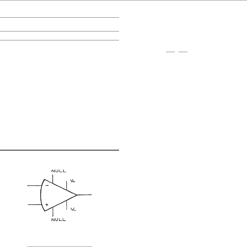
A
CM
(often expressed in dB). The output of an opera-
tional amplifier is A
D
times the differential voltage
plus A
CM
times the common mode voltage. For arbi-
trary voltages v
1
and v
2
at the two amplifier inputs, the
differential voltage is (v
1
– v
2
)/2 and the common
mode voltage is (v
1
þ v
2
)/2. For the 741, the 90 dB
value of the CMRR means that a 1 V signal at each
input terminal will result in a 32 lV output signal.
This is sho wn in the following calculation:
90 dB ¼ 20 log
A
D
A
CM
;
A
D
A
CM
¼ 10
4:5
¼ 3:2310
4
ð6:32Þ
Since the differential voltage is 0 V, the output voltage
will be the common-mode voltage multiplied by the
common-mode gain A
CM
. For a common-mode voltage
of 1.0 V, the output voltage is then 1.0/(3.2 3 10
4
) ¼
32 3 10
6
V.
Open-loop d.c. gain. This is the gain in the absence of a
connection from output to input – that is, in the
absence of any feedback. The gain of the amplifier
in the presence of a feedback network is called the
closed-loop gain. With open-loop gains of the order
of 200,000 or more, it can be seen that the region of
linear operation applies to only very small input sig-
nals. At a gain of 200,000, an input signal of þ75 lV
is sufficient to drive the output to þ15 V, the max-
imum possible level.
Frequency response. This is given in terms of either
the GBWP or the frequency at which the gain equals
0 dB (unit gain). The two methods give nearly the
same numbers for a single-pole transfer function.
For the 741, at 1 MHz the gain has fallen by over
five orders of magnitude from the d.c. value. It
should be kept in mind that these frequency-
response data are based on so-called small-signal
conditions, where the input is small enough so that
the output stages are operating well within their lin-
ear region.
Slew rate. This gives the time response of the amplifier
to large input signals. For this specification the
amplifier is connected in a unit-gain (closed-loop)
configuration with negative feedback, and an input
voltage step is applied. The slew rate is then taken as
the ratio of the amplitude of the input voltage to the
rise time for the output voltage waveform. For the
741, the slew rate is 0.5 V/ ls.
Input resistance. This is the resistance R
i
between the
input terminals with one terminal grounded.
Table 6.22 Comparison of Operational Amplifier
Parameters
a
Electrical Properties 741 OP07
CMRR (dB) 90 120
Open-loop d.c. gain 200 000 500 000
GBWP (MHz) 1.5 0.6
Slew rate (V/ls) 0.5 0.3
Input resistance (MX)280
Output resistance (X)7560
Input offset
voltage (mV)
5 0.010
Input offset
current (nA)
20 0.3
Input bias
current (nA)
80 0.7
Input voltage
range (V)
613 613
Maximum peak-to-peak
output voltage swing (V)
28 25
Power-supply
rejection ratio (lV/V)
150 5
Power consumption (mW) 50 75
a
Typical characteristics at 25 °C with power-supply voltages
of 615 V:
Figure 6.64 Schematic symbol
for the operational amplifier,
showing input, output, power
supply, and null terminals.
426 ELECTRONICS

Output resistance. This is the resistance R
o
(seen by the
load) between the output terminal and ground. It
determines whether the amplifier approximates a
voltage or a current source.
Input offset voltage. This is the d.c. voltage V
IO
that
must be applied across the input terminals to bring
the d.c. output to zero. For the 741 it is 0.8 mV and
can be compensated for. The 741 is not a good
choice for the amplification of millivolt d.c. levels.
Input offset current (I
IO
). This is the difference between
the currents into the input terminals necessary to
bring the output voltage to zero.
Input bias current (I
IB
) This is the average of the currents
into the input terminals with the output voltage at zero.
It should be noted that these bias currents will flo w
through circuit elements (generally resistors) attached
to the input terminals. If the resistances are not identical,
voltage differences will be developed across the input
terminals and amplified along with the input signal.
Input voltage range (V
I
). The maximum allowed input
voltage for which proper operation can be maintained.
Maximum peak-to-peak output voltage swing. The
maximum peak-to-peak output voltage that can be
obtained without clipping about a quiescent output
voltage of zero.
Power-supply rejection ratio. The change in input offset
voltage for a given change in power-supply voltage.
Operational amplifiers are particularly good in this
regard and do not require highly regulated power
supplies.
Temperature effects. The various offset and bias cur-
rents and voltages are temperature dependent. The
variations of these parameters with temperature are
specified by temperature coefficients.
The 741 is internally compensated with a capacitor at
the high-gain second stage to produce a pole in the transfer
function at 6 Hz. This ensures stable operation under even
100% feedback conditions (of course, this gain in stability
reduces the high-frequency response of the amplifier). Two
extra terminals are available for connection to an external
10 kX potentiometer, the wiper arm of which is connected
to the negative power supply. By adjusting the potentiom-
eter, the input offset voltage can be eliminated. Additional
features include short-circuit output protection and input
overload protection. Single amplifiers come in at least four
different packages: an 8 lead metal can, a 14 lead dual in-
line package (DIP), an 8 lead mini-DIP, and a 10 lead Flat
Pak. There is a commercial model – the 741C – that oper-
ates over a restricted temperature range, and a military
model – the 741A – that operates over an extended temper-
ature range. The 741 sells for about the price of a few
1/4 W composition resistors.
The OP07 is a premium grade operational amplifier with
a very low input offset voltage, obtained by trimming thin-
film resistors in the input circuit. The low offset voltages
usually eliminate the need for external null circuits. The
OP07 also has low input bias current and high open-loop
gain. It is a direct pin-for-pin replacement for the 741.
Some examples of more specialized operational amplifiers
are given in Table 6.23.
Because
of their high gain, wide bandwidth, and small
offsets, operational amplifiers with suitable feedback net-
works can perform a wide range of electronic functions.
There are many excellent texts devoted to operational-
amplifier applications.
4
Here we give only a list of the
basic configurations. In all of these it is important to keep
in mind the following design rules:
(1) The offset-voltage temperature coefficient must pro-
duce voltages much less than the input signal through-
out the anticipated temperature range. The offset
voltage can be eliminated with an external nulling
circuit at any given temperature, but variations with
temperature cannot be easily accommodated.
(2) The voltages created by the bias currents flowing through
resistances attached to the input terminals must be less
than the signal voltage. For high output-impedance
Table 6.23 Some special operational amplifiers
Low offset voltage OP07
Low bias current (Harris) HA-5180
High voltage (Harris) HA-2640/45
Low power consumption (National) LF441
Single-power-supply
operation
(National) LM10
Wide bandwidth (National) LM318
(Burr-Brown) OPA606
Video preamplifier 733
AMPLIFIERS AND PULSE ELECTRONICS 427
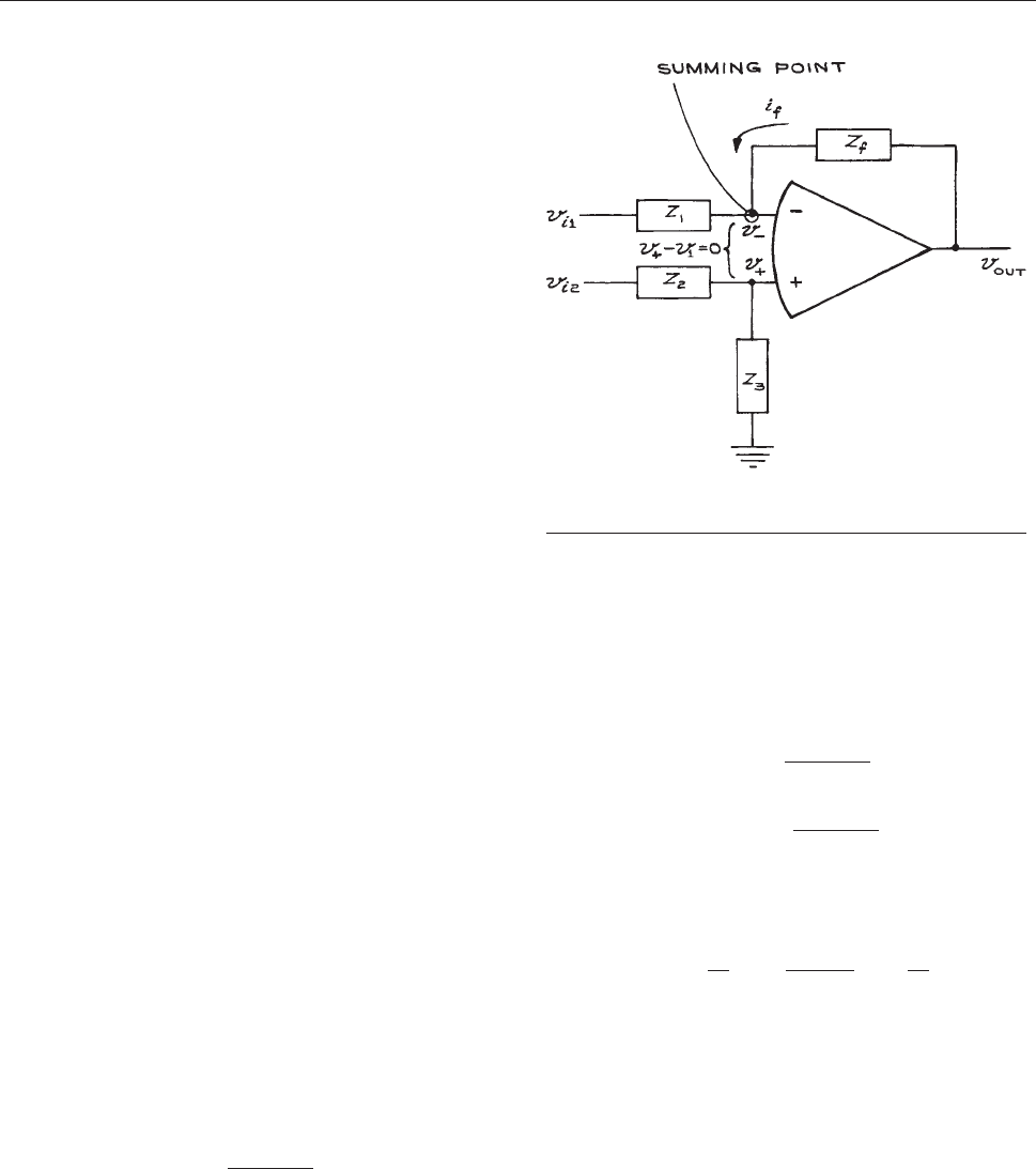
sources this may create a problem, but it can be solved by
introducing an intermediate buf fer stage with a high
input impedance (so as not to load the source) and a
low output impedance (to minimize the ef fects of input
bias current). The temperature coeffi cient of the offset
current must produce of fset voltages much less than the
signal voltage over the anticipated temperature range. To
minimize bias-current effects, the resistances to ground
from both input terminals should be identical.
(3) Frequency response and compensation must prevent
the amplifier from breaking into oscillation. The 741
is internally compensated. High-frequency amplifiers
lack internal compensation, but have extra terminals
for external compensation circuits.
(4) The maximum rate of change of a sinusoidal output
voltage V
0
sin xt is V
0
x. If this exceeds the slew rate
of the amplifier, distortion will result. Slew rate is
directly related to frequency compensation, and high
slew rates are obtained with externally compensated
amplifiers using the minimum compensation capaci-
tance consistent with the particular configuration. Data
sheets should be consulted.
6.4.3 Operational-Amplifier
Circuit Analysis
If ideal behavior can be assumed (as is reasonable for circuits
where the open-loop gain is much larger than the closed-loop
gain), only the following two rules need be used to obtain the
transfer function of an operati onal-amplifier circuit, as
shown schematically in Figure 6.65:
(1)
The voltage across the input terminals is zero.
(2) The currents int o the input terminals are zero (the invert-
ing terminal is sometimes called the summing point).
Applying these to the generalized circuit of Figure 6.65,
we
see that the voltage at the þinput is v
i2
Z
3
/(Z
2
þZ
3
), since
there is no current flowing into the þ input and Z
2
, Z
3
form a
voltage di vider. From Rule 1, the voltage at the input must
also equal v
i2
Z
3
/(Z
2
þ Z
3
). The current through Z
1
is then the
potential diff erence across it div ided by Z
1
,or:
v
i1
v
i2
Z
3
ðZ
2
þ Z
3
Þ
=Z
1
ð6:33Þ
This current must be equal in magnitude and opposite in
sign to the current from the output through the feedback
element Z
f
. This current, i
f
, is given by the potential differ-
ence across Z
f
divided by Z
f
:
i
f
¼ v
out
v
i2
Z
3
ðZ
2
þ Z
3
Þ
=Z
f
¼ v
i1
v
i2
Z
3
ðZ
2
þ Z
3
Þ
=Z
1
ð6:34Þ
Solving for v
out
, we obtain:
v
out
¼v
i1
Z
f
Z
1
þ v
i2
ð
Z
3
Z
2
þ Z
3
Þð1 þ
Z
f
Z
1
Þð6:35Þ
Some useful configurations are illustrated in Figure 6.66.
Th
e summer circuit [Figure 6.66(e)] is an elaboration of the
in
verting amplifier , with the current into the summing point
coming from two external sources (v
A
and v
B
)canceledbythe
current from the feedback loop, v
out
/R
f
.IfR
A
¼ R
B
¼ R,then
v
out
¼(R
f
/R)(v
A
þv
B
). If R
A
¼ R
B
,thenv
out
is equal to the
negati ve of the weighted sum of voltages v
A
and v
B
,thatis:
Figure 6.65 The general operational-amplifier circuit.
Power supply and null terminals not shown.
428 ELECTRONICS
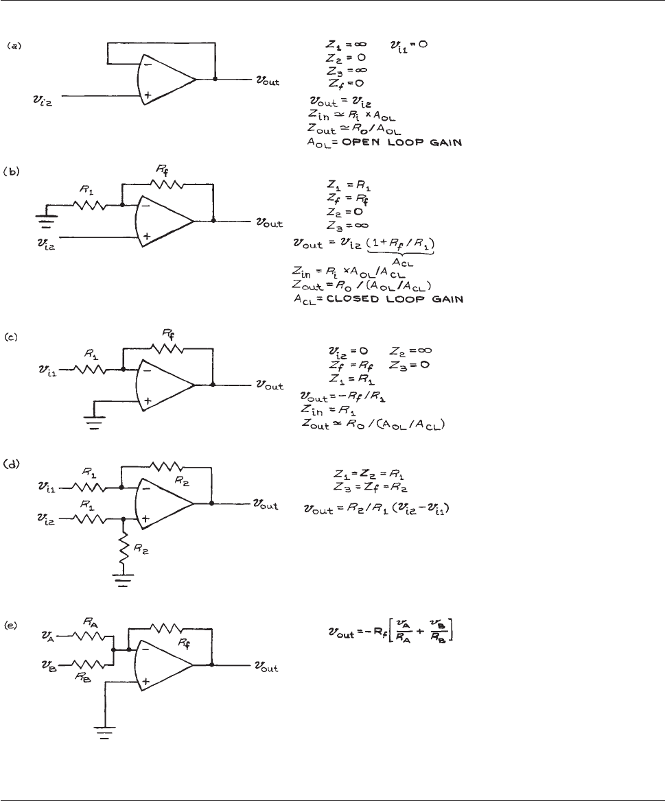
Figure 6.66 Operational-amplifier configurations: (a) follower; (b) follower with gain; (c) inverting amplifier; (d) subtractor;
(e) summer; (f) low-pass filter (integrator); (g) high-pass filter (differentiator); (h) logarithmic amplifier; (i) precision rectifier;
(j) clamp. The parameters are defined in Figure 6.59.
AMPLIFIERS AND PULSE ELECTRONICS 429
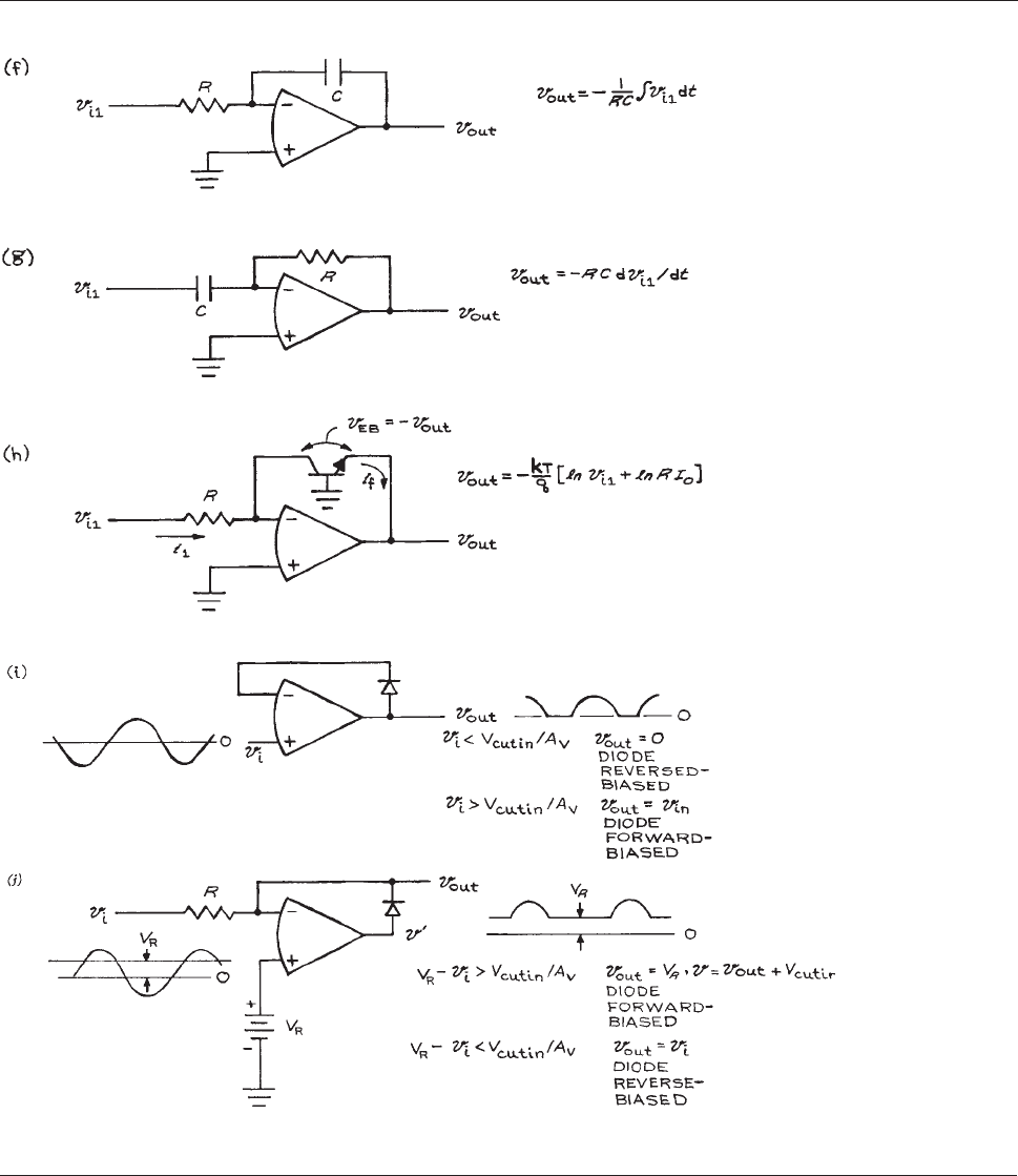
Figure 6.66 (cont.)
430 ELECTRONICS

v
out
¼ ½ð
R
f
R
A
Þv
A
þð
R
f
R
B
Þv
B
ð6:36Þ
Any number of external signal sources can be summed
in this way.
A sinusoidal input to the low-pass filter [Figure 6.66(f)]
gi
ves v
out
¼ðjxRCÞv
i1
. For a nonsinusoidal input, the cur-
rent into the summing point from v
i1
is v
i1
/R, because the
in v erting input is at ground (rule 1). Often one speaks of the
inverting input being at virtual ground. Although there is
no direct connection from the inverting input to ground,
the condition in which both inputs are at the same poten-
tial results in the inverting input assuming a potential of
zero when the noninverting input is at g round potential.
The current through the fe edback capa citor of this circuit
is i
f
, and the voltage across the capacitor, v
out
is equal to
ð1=CÞ
R
i
f
dt.Sincei
f
and v
i1
/R are equal in magnitude and
opposite in sign:
v
out
¼ð1=CÞ
Z
i
f
dt ¼ð1=RCÞ
Z
v
i1
dt: ð6:37Þ
and the circuit acts as an integrator of the input voltage.
Integration times of several minutes or even hours are
possible with high quality, low-leakage capacitors and
operational amplifiers with small offset voltages and bias
currents.
For the high-pass filter [Figure 6.66(g)], v
out
¼
RC(dv
il
/dt) and the circuit acts as a differentiator.
The integrator and differentiator circuits are simple
forms of active filters. More complex networks involving
only capacitors and resistors can be used to obtain poles in
the left half of the complex s-plane, which in the past were
only obtained with inductors in passive filter networks.
The operational amplifier allows the use of reasonable
resistor and capacitor values even at frequencies as low
as a few hertz. An additional advantage is the high isola-
tion of input from output due to the low output impedance
of most operational-amplifier circuits. The limitations of
active filters are directly related to the properties of the
operational amplifier. Inputs and outputs are usually sin-
gle-ended and cannot be floated as passive filters can. The
input and output voltage ranges are limited, as is the output
current. Offset currents and voltages, bias currents, and
temperature drifts can all affect active filter performance.
A good introduction to active filters is the Active Filter
Cookbook by D. Lancaster.
The circuits in Figure 6.66(b) to (g) are examples of the
use
of operational amplifiers in analog computation. With
these circuits, the mathematical operations of addition,
subtraction, multiplication by a constant, integration, and
differentiation can be performed. Multiplication or divi-
sion of two voltages is accomplished by a logarithmic
amplifier, an adder (for multiplication) or subtractor (for
division), and an exponential amplifier.
Both the logarithmic and exponential amplifiers rely on
the exponential I–V characteristics of a p–n junction. When
this junction is the emitter–base junction of a transistor, the
collector current I
C
with zero collector–base voltage is:
I
C
¼ I
0
½expðqV
EB
=gkTÞ1ð6:38Þ
where I
0
is a constant for all transistors of a given type, V
EB
is the emitter–base voltage, q is the electron charge and g is
a constant, 1 for Ge and 2 for Si. Typically, I
0
is 10 to 15
nA for silicon planar transistors.
For I
C
> 10
8
A, the equation reduces to I
C
¼I
0
exp(qV
EB
/
gkT). For the configuration shown in Figure 6.66(h), i
1
¼ v
il
/
R ¼ I
0
exp(qv
out
/gkT)andv
out
¼ðgkT=qÞðln v
i1
þ ln RI
0
Þ.
Since k, T, q, g, R, and I
0
are constants, v
out
will be propor-
tional to v
i1
. Practical logarithmic amplifiers can operate
over three decades of input voltages. They do, however,
need temperature-compensating circuits that generally
require the use of matched pairs of transistors. In addition
to their arithmetic use, logarithmic amplifiers are fre-
quently used for transforming signal amplitudes that cover
orders of magnitude to a linear scale. Exponential (anti-
logarithmic) amplifier circuits are logarithmic circuits with
the input and feedback circuit elements interchanged.
Logarithmic and exponential amplifiers are examples of
nonlinear circuits – the output is not linearly related to the
input. Operational amplifiers are used extensiv ely in non-
linear circuits. Because the cutin voltage of simple diodes
is a few tenths of a volt (0.2 V for Ge and 0.6 V for Si), they
cannot be used to rectify milli volt-level a.c. voltages. A
diode in the feedback loop of an operational amplifier [see
Figure 6.66(i)] results in a rectifier with a cutin volt age equal
to
the diode cutin voltage divided by the open-loop gain of
the amplifier. With a slight modification, the rectifier circuit
canbeconvertedtoaclamp [see Figure 6.66(j)] in which the
AMPLIFIERS AND PULSE ELECTRONICS 431
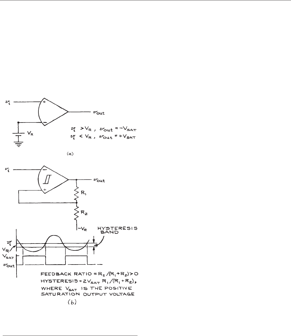
output follows the input for voltages greater than a reference
voltage V
R
, but equals V
R
for input voltages less than V
R
.
Comparator circuits are used to compare an input signal
with a reference voltage level. The output is driven to V
þ
or V
depending on whether the input is less than or
greater than the reference level [see Figure 6.67(a)]. Using
an
amplifier in such a saturated mode is very poor practice
and practical comparators with internally clamped outputs
less than V
þ
and V
are available. The LM311 is a
common example. The transition between the two output
states can be accelerated by the use of positive feedback
[Figure 6.67(b)]. Such a circuit is called a Sc
hmitt trigger
and finds wide application in signal conditioning when it is
necessary to convert a slowly changing input voltage into
an output waveform with a very steep edge. The price paid
for the fast transition is hysteresis – where the threshold
voltage for a positive transition of the output is different
from the threshold voltage for a negative transition. Hys-
teresis inhibits the output from oscillating between the two
output states when the input is very close to the threshold
level.
6.4.4 Instrumentation and
Isolation Amplifiers
Instrumentation amplifiers are used for amplifying low-le v el
signals in the presence of large common-mode voltages, as,
for example, in thermocouple and bridge circuits. The instru-
mentation amplifier is dif ferent from the operational ampli-
fier; the feedback network of the instrumentation amplifier is
integral to it and a single external resistor sets the gain. The
output of the instrumentation amplifier is usually single-
ended with respect to ground and is equal to the gain multi-
plied by the dif ferential input vol tage. Compared to an
operational amplifier in the differential configuration with
equiv alent gain, the instrumentation amplifier has a higher
common-mode rejection ratio and higher input impedance.
Instrumentation amplifiers are often made up of three opera-
tional amplifiers, as shown in Figure 6.68. Amplifiers A1 and
A2
together provide a differential gain of 1 þ 2R
1
/R
G
and a
common-mode gain of unity. Amplifie r A3 is a unit-gain dif-
ferential amplifier. Amplifiers A1 and A2 operate as follo wers
with gain, and resistors R
1
do not af fect the input impedances.
Because amplifier A3 is driven by the low output impedances
of Al and A2, the resistors R
o
can hav e rel ativ ely small values
in order to optimize CMRR and frequency response while
minimizing the ef fects of input of fset currents.
The three-amplifier configuration is limited to common-
mode voltages of 68 V in most applications. Typical high-
performance instrumentation amplifiers are the 1NA110
(Burr-Brown), LH0038 (National Semiconductor), and
AD624 (Analog Devices). Typical specifications for
high-performance amplifiers are given in Table 6.24.
Instrumentation
amplifiers cannot be used when the
common-mode voltage exceeds the power-supply voltage.
Figure 6.67 (a) Simple comparator (V
sat
and +V
sat
are the
minimum and maximum voltages the amplifier can deliver;
V
R
is a constant reference voltage); (b) Schmitt trigger
(comparator with positive feedback).
432 ELECTRONICS
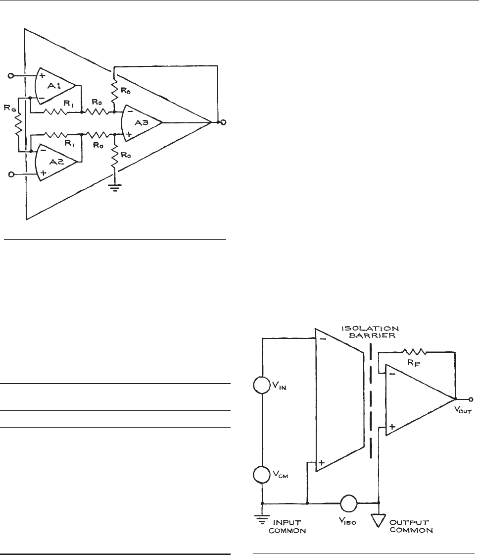
In these cases, an isolation amplifier is required. Isolation
amplifiers are also useful when the input and output signals
of an amplifier are referenced to different common voltage
levels. It is often necessary, for example, to impose a low-
voltage waveform on a d.c. high voltage. With an isolation
amplifier, the modulation voltage can be derived from a
source referenced to ground and the amplifier output can
be referenced to the d.c. high voltage. The internal con-
struction of the amplifier isolates the high-voltage output
from the low-voltage input.
The basic isolation-amplifier configuration is shown in
Figure 6.69. For the above example, V
IN
is the modulation
voltage referred to ground (V
CM
¼ 0), and V
ISO
is the high
voltage modulated by V
IN
. In cases where V
CM
exceeds
610 V, the input common terminal is not grounded and
the common-mode voltage is referenced to the output com-
mon terminal. This effectively transfers V
CM
across the
isolation barrier and allows for V
CM
voltages up to the
maximum isolation rating of the amplifier.
The isolation-mode rejection ratio (IMRR)andCMRR
are critical isolation-amplifier parameters because of the
large common-mode and isolation voltages present. To cal-
culate the effect of common-mode and isolation voltages on
amplifier performance, it is necessary to add the product of
IMRR and V
ISO
, and that of CMRR and V
CM
to V
IN
. Typical
values of IMRR and CMRR are 140 and 90 dB, respec-
tively. For an IMRR of 140 dB, a 1 kV isolation voltage
produces the equivalent of 0.1 mV at the input terminals
of the amplifier. Other important parameters specific to iso-
lation amplifiers are the maximum isolation voltage, isola-
tion resistance, and isolation capacitance.
Figure 6.68 Three-amplifier instrumentation amplifier.
Table 6.24 Typical high-performance instrumentation
amplifier specifications
1NA110 LH0038 AD624
Gain range 1–500 1–2000 1–1000
Gain nonlinearity (%) 0.001–0.01 0.001 0.001
Input impedance (X)53 10
12
5 3 10
6
10
9
CMRR (dB) 90110 120 130
Input offset-voltage
drift (lV/°C)
2 0.25 0.25
Input bias
current (nA)
0.050 50 50
Bandwidth (MHz) 2.5 2 25
Noise, referred to input
(nV/
ffiffiffiffiffiffi
Hz
p
)
10 6 4
Figure 6.69 Isolation amplifier.
AMPLIFIERS AND PULSE ELECTRONICS 433
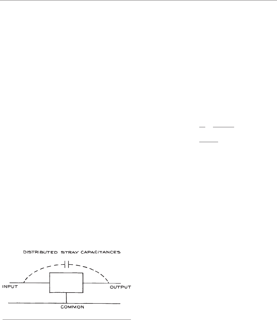
Isolation between input and output is achieved with opti-
cal couplers or transformers. The latter are more expensive,
but have higher isolation voltage ratings and IMRR. An
additional advantage of the transformer-coupled amplifiers
is their built-in isolated power supply. The input and output
stages of the optically coupled amplifiers must have sepa-
rate power supplies. This means that the output-stage power
supplies must be floated at the isolation voltage. Burr-
Brown manufactures a full line of isolation amplifiers for
medical and industrial applications. The 3450 and 3656
series are transformer-coupled, while the 3650 and
150100 series are optically coupled. Prices range from tens
to hundreds of dollars, depending on specifications. Analog
Devices produces a premium transformer-coupled isolation
amplifier, the AD295, as well as the less expensive AD202.
6.4.5 Stability and Oscillators
For circuits composed only of passi ve elements, the poles of
the transfer function will always lie on the left-hand side of
the complex s ¼ r þ jx plane, that is, will always be less
than zero. For circuits with acti v e elements, this is not nec-
essarily the case. If, for example, a fraction of the output
signal of an amplifier is returned to the input in phase with
the original input signal, an unstable situation will result and
the output of the amplifier will increase with time. Analysis
of such a circuit will show at least one pole to lie in the
positiv e half of the complex s-plane. Unwanted oscillations
in amplifiers are due to the regenerative coupling of a frac-
tion of the output signal back to the input (see Figure 6.70).
Stray
capacitances between input and output may be suffi -
cient at high frequencies to couple the output signal back to
the input. This can be minimized by having the output and
input physically separated as far apart as possible. A copper
shield separating the output and input is often also effective,
and high-frequenc y circuits built on printed circuit boards
should have generous ground-plane areas.
While the lack of stability is undesirable in amplifiers,
sinusoidal oscillators depend on such instabilities for their
operation. Consider an amplifier with gain A
o
(it can be any
one of the four already considered). If X
o
represents the
output signal (a current or voltage) and X
i
the input signal
(also a current or voltage), X
o
¼ A
o
X
i
. For a simple ampli-
fier X
i
¼ X
s
(the source signal).
If a fraction b of the output is sent back to the input
in such a way as to cancel part of the source signal, the new
signal X
i
is X
s
bX
o
, and the gain of the amplifier with
feedback is the output signal divided by the source signal:
A
f
¼
X
o
X
s
¼
X
o
X
i
þ bX
o
A
f
¼
A
o
1 þ bA
o
ð6:39Þ
For b > 0, the feedback signal acts to cancel the signal
from the source and A
f
< A
o
.Thisiscalledne gative or de gen-
erative feedback and is frequently used to stabilize amplifier
gain and improve linearity and noise. For b < 0, the feedback
signal adds to the source signal at the input and A
f
> A
o
.This
is positive or r egenerative feedbac k and is sometimes used to
increase the gain of amplifiers at the expense of stability. If
bA
o
¼1, A
f
¼ N and the amplifier is unstable, with an
output that breaks into oscillation or saturates.
In practice, both A
o
and b are frequency dependent and
the response of such feedback amplifiers can be calculated.
If only stability criteria are desired, it is only necessary to
determine whether any poles of the transfer function lie in
the right half of the complex plane.
One will have an oscillator if bA
o
can be made equal to
1 for only a single frequency, by means of a frequency-
selective feedback network. There are a large number of
frequency-selective circuits based on LC and RC networks.
Quartz crystal oscillators are particularly stable and free of
temperature effects. These devices work by the application
of a potential difference across the faces of a quartz crystal
that becomes deformed and oscillates at a resonant fre-
quency determined by the size and orientation of the crys-
tal planes with respect to the electrodes. Crystal oscillators
Figure 6.70 Unwanted feedback from stray capacitance.
434 ELECTRONICS
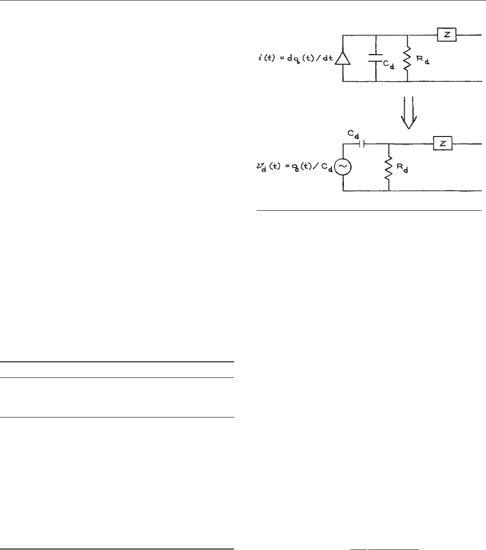
with Q values of 10
4
to 10
6
at frequencies from tens of kHz
to over 100 MHz are commercially available in DIP and
SMT configurations.
6.4.6 Detecting and Processing Pulses
There is a large class of experiments, especially in nuclear
and particle physics, that deals with the detec tion an d
analysis of single events . With the advent of detectors
for low-energy photons, electrons, and ions, these techni-
ques have sp read to the fields of atomic and molecular
physics, chemistr y, and biology. Commercial inst rumen-
tation is widely available, but to s pecify and use the units
to best advantage a knowledge of the basic properties of
the detectors, amplifiers, and associated processing cir-
cuits is required.
Table 6.25 summarizes the properties of the more common
types
of detectors. The first part of the table allo ws one to
estimate the output of a given detector for an arbitrary input.
A 5 MeV alpha particle depositing all its energy in a silicon
detector, for example, will create 1.4 3 10
6
electron–hole
pairs. W ith a suitable bias across the detector , the charge
can be collected in 0.1 to 10 ns. Similar considerations allow
one to calculate the outputs of other detectors. The detectors
can be represented electrically by the equiv alen t circuit of
Figure 6.71. The choice of preamp lifier, amplifier , and shap-
ing
and analysis circuits now depends on the information to
be obtained from the pulse. Figure 6.72 sho ws the arrange-
ment
of three general categories of experiments – counting,
timing, and pulse-height analysis. Each one has different elec-
tronics requirements, but before considering these systems in
detail it is worthwhile to examine the circuits commonly
available for amplification and shaping.
Preamplifiers can be v oltage, current, or charge-sensiti v e.
Voltage preamplifiers are not generally used, because the
voltage generated by most detectors depends on the capaci-
tance of the detector (Figure 6.73) that can change with bias
v
oltage and other circuit parameters. Current preamplifiers
have lo w input impedances and are designed to conv ert the
fast current pulse from a photomultiplier or electron multi-
plier to a voltage pulse. Their sensiti vity is specified as out-
put millivolts per input milliampere. Char ge-sensiti v e
preamplifiers are the most commonly used preamplifi ers
because their gain is independent of the capacitance of the
detector. Their sensitivity is specified in output milli v olts per
unit input charge or in equivalent output milliv olts per MeV
deposited in a giv en solid-state detector.
A schematic diagram of a combined detector and
charge-sensitive preamplifier is shown in Figure 6.73.
Neglecting
the effect of the coupling capacitor, the Laplace
transform of the output voltage v
o
(s) is:
v
o
ðsÞ¼
qðsÞ
C
f
1
1 þ 1=R
f
C
f
s
ð6:40Þ
Table 6.25 Particle Detectors
Particle
Detector
Output Signal Charge-
Collection
Time
Semiconductor:
Ge
Si
1 electronhole pair=2:8eV deposited
1 electronhole pair=3:5eV deposited
o
0.110 ns
a
Photomultiplier 10
6
10
7
electrons/photoelectron 1 ns
Electron
multiplier
10
6
10
8
electrons/incident
electron
0.51ns
Microchannel
plate
10
3
10
4
electrons/incident
electron
0.1 ns
Scintillator:
Plastic
Alkali halide
1 photon/3keV deposited
0:110 ns
1 ls
Gas-filled tube 1 ion pair/25–35eV deposited 0.015 ls
a
For narrow depletion depth.
Figure 6.71 Equivalent circuit of a detector.
AMPLIFIERS AND PULSE ELECTRONICS 435
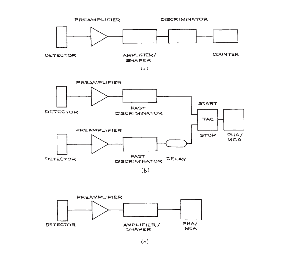
The function has a pole at s ¼1/R
f
C
f
; the Bode plot is
given in Figure 6.74. The high-frequency pole at x
2
is a
result of the preamplifier transfer function. The output wave-
form for a rectangular input pulse of duration s will be a tail
pulse of rise time s, amplitude q/C
f
, and decay time R
f
C
f
.
For very small values of s, the rise time of the output
pulse will be determined by the characteristics of the
amplifier itself. Practical amplifiers use high-stability
NPO capacitors for C
f
with values from 0.1 to 5 pF; the
feedback resistor R
f
is made as large as is consistent with
the signal rate and leakage current. Noise in charge-
sensitive preamplifiers is specified in terms of the energy
resolution FWHM in keV. This can be converted to an
equivalent charge noise with the factors in Table 6.25.
T
o test charge-sensitive preamplifiers, the circui t of Fig-
ur
e 6.75 can be used. An input step voltage applied to
Figure 6.72 Three categories of pulse experiments: (a) counting, (b) coincidence, and
(c) pulse-height analysis.
436 ELECTRONICS
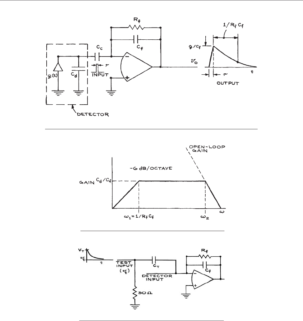
Figure 6.73 Combined detector and charge-sensitive preamplifier.
Figure 6.74 Bode plot for a charge-sensitive preamplifier.
Figure 6.75 Test circuit for charge-sensitive preamplifiers.
AMPLIFIERS AND PULSE ELECTRONICS 437
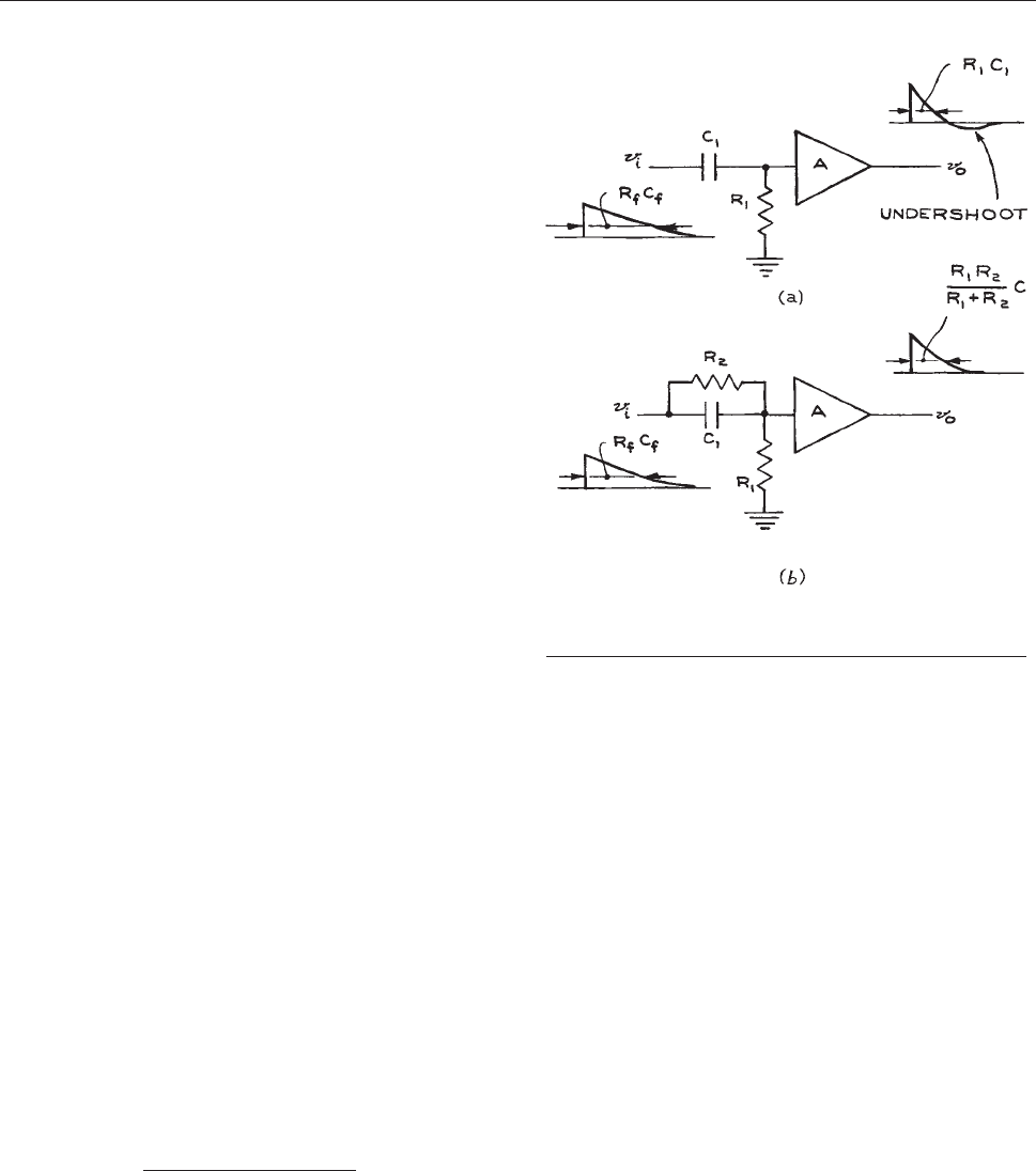
the capacitor C
T
results in an amount of charge equal to
C
T
V
T
deposited on the input of the preamplifier. For
10
15
CwithC
T
¼ 10 pF, the amplitude of the input
voltage pulse must be 10 mV. The 50 ohm resistor in the
circuit is for te rmination purposes. The duration of the test
input current will be equal to the rise time of the voltage
input.
The output pulses from the preamplifier are generally
very different in shape from the input signals. This is the
case even with fast-current preamplifiers. An important
function of the amplifier and shaping circuits is to increase
the amplitude of the preamplifier output signal and change
its shape to minimize pulse overlap and optimize the sig-
nal-to-noise ratio. To minimize pulse overlap, the duration
of the pulses should be short compared with the average
time between them. In more quantitative terms, the rms
voltage level of the pulse train to be processed should
be much less than the required voltage resolution of the
system. If n is the pulse rate and v(t) is the functional form
of the pulse, then:
v
rms
¼ n
ð
‘
0
vðt Þ
2
dt
2
4
3
5
1=2
ð6:41Þ
For rectangular pulses of unit height and width s:
v
rms
¼ n
1=2
s
1=2
ð6:42Þ
The long-tail puls e from a charge-sensitive preamplifier
can be shortened with a differentiating circuit [Figure
6.7
6(a)]. The circuit reduces the fall time from R
f
C
f
to
RC. A disadvantage of simple differentiation is
undershoot, which appears on the trailing edge of the out-
put pulse. This can be substantially eliminated by modify-
ing the transfer function of the differentiating circuit to
include a zero that exactly cancels the pole in the pream-
plifier transfer function [Figure 6.76(b)]. The Laplace
transfor
m of the transfer function of Figure 6.76(b) is:
s þ 1=R
2
C
1
s þðR
1
þ R
2
Þ=ðR
1
R
2
C
1
Þ
ð6:43Þ
If R
2
C
1
is set equal to R
f
C
f
from the preamplifier, under-
shoot can be eliminated. This technique of pole-zero com-
pensation is commonly used in pulse shaping.
For pulse-height analysis, a Gaussian waveform has the
best noise characteristics.
5
Such a shape can be obtained
from a tail pulse by a single differentiation and an infinite
number of cascaded integrations with integration time con-
stants all equal to the differentiation constant. In practice,
four integrations give a shape very close to Gaussian.
Bipolar pulses can be obtained by double differentiation
of a tail pulse with an intermediate integration (Figure
6.77). An important property of the bipolar pulse is that
the
zero crossing always occurs at a fixed time after its
start, determined by the time constant, and is independent
of pulse height. When used with zero-crossing discrimina-
tors, such pulses permit reliable timing to be accomplished
with long-decay-time pulses. Bipolar pulses, however,
have poorer noise characteristics than unipolar Gaussian
pulses.
Figure 6.76 Differentiating circuits: (a) without pole-zero
compensation; (b) with pole-zero compensation.
438 ELECTRONICS
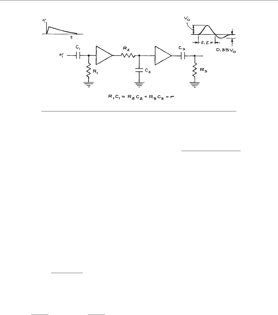
An alternative to RC shaping is delay-line shaping. The
equivalent of unipolar and bipolar pulses can be obtained
with single- and double-delay-line circuits (Figure 6.78).
Adv
antages are the preservation of fast rise times, sharp
trailing-edge clipping, and greatly reduced base-line shifts.
These advantages are offset by the poor noise properties of
the pulses compared with RC shaping. Delay-line shaping
is mostly confined to timing applications.
The shaping circuits discussed in the previous paragraph
are generally incorporated in the variable-gain main ampli-
fier that follows the preamplifier. While noise is a consid-
eration with such amplifiers, it is not so critical as with
preamplifiers because of the larger signal levels. Important
considerations are linearity and fast overload recovery. To
reduce baseline shifts from pulse pileup, main amplifiers
often incorporate a baseline restorer circuit. The principle
of operation is illustrated in Figure 6.79. A noninverting
am
plifier with gain
HðsÞ is placed in the negative-feedback
loop of an amplifier with gain
GðsÞ. The Laplace transform
of the transfer function for the system is:
GðsÞ
1 þ
GðsÞ
HðsÞ
ð6:44Þ
If both
GðsÞ and
HðsÞ are themselves transforms of
single-pole transfer functions, given by:
GðsÞ¼
A
1 þ T
1
s
and
HðsÞ¼
K
1 þ T
2
s
ð6:45Þ
where A and K are the mid-band gains of the amplifiers, the
overall transfer function is:
Að1 þ T
2
sÞ
AK þð1 þ T
1
sÞð1 þ T
2
sÞ
ð6:46Þ
At high frequencies (s >> 1) the transfer function reduces
to
GðsÞ, while for d.c. (s ¼ 0) the function is 1/K. The
overall effect of the circuit is to amplify high-frequency
pulses while attenuating low-frequency baseline shifts.
For counting applications, the principal considerations
are pulse rate and discriminator setting. The shaped pulses
from the amplifier should be sufficiently short in duration
to avoid pileup and baseline shifts. A leading edge dis-
criminator can be used with a unipolar pulse. Since such
units are based on regenerative (positive-feedback) com-
parator circuits that have hysteresis, the decay of the input
pulse must not pass through the recovery voltage level
until the triggered state is attained. When bipolar pulses
are to be counted, zero-crossing discriminators should be
used.
Timing systems require that the leading-edge information
from the detector pulse be faithfully preserved. Timing
errors can arise from due time variations in the processed
pulses relative to the input pulse, long-term drift from com-
ponent aging, and noise. Wide-band current preamplifiers
and fast timing amplifiers with short integrating and differ-
entiating shaping circuits or delay-line shaping should be
used. When using wide-band amplifiers, precautions should
Figure 6.77 Bipolar pulse shaping with CR–RC–CR circuits.
AMPLIFIERS AND PULSE ELECTRONICS 439
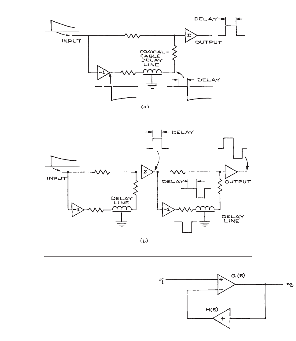
be taken to electrically terminate all connections properly
and avoid stray capacitances that can form positive-feed-
back paths and produce instability. When the detector signal
itself is of sufficient amplitude – as it is for the output of a
photomultiplier tube used with a scintillation detector – a
timing signal can be taken directly from the detector without
further amplification or shaping. Leading-edge and con-
stant-fraction discriminators are most commonly used for
timing. The constant-fraction discriminator provides the
Figure 6.78 (a) Unipolar and (b) bipolar pulse shaping with delay lines.
Figure 6.79 A baseline restorer circuit.
440 ELECTRONICS
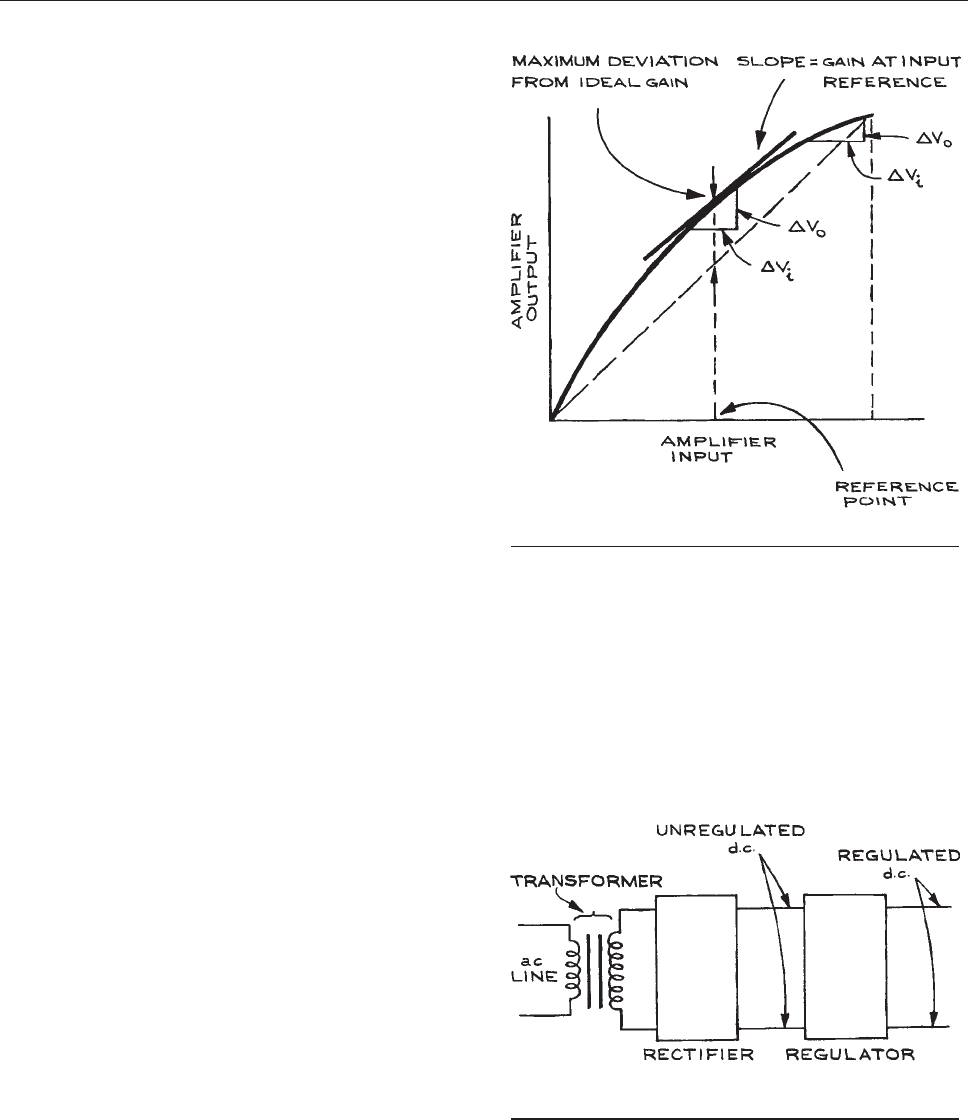
better resolution times. With this discriminator, the input
signal is delayed and combined with a fixed fraction of the
undelayed signal. A bipolar pulse with a zero crossing
independent of rise time and amplitude results can be used
to activate a zero-crossing detector.
In Figure 6.72(b), the delay inserted in the stop li
ne of the
system is to ensure that the stop pulse to the time-to-ampli-
tude conv erter (TAC) will always follow the start pulse. The
TA C conv erts the time difference between the start and stop
input pulses to a single pulse of an amplitude proportional to
the time dif ference. High quality, low-attenuation coaxial
cable makes an excellent delay line, and lumped-parameter
delay lines are also commercially av ailable. Timing informa-
tion is usually obtained by processing the output of the TA C
with a pulse-height analyzer (PHA). A more direct method is
with a time-to-digital con v erter that con v erts the time differ-
ence between the start and stop pulses to a digital word for
processing. Depending on detector characteristics, time res-
olution of pico-seconds can now be obtained.
Particle-spectroscopy experiments rely on the preservation
of the pulse-amplitude information from the detector because
the amplitude is a direct measure of the particle ener gy. Opti-
mum amplitude resolution is obtained by operating the pre-
amplifier and amplifier in their linear ranges, reducing
sources of noise and baseline shifts from pileup, and using
semi-Gaussian pulse shapes as inputs to the PHA. The func-
tion of the PHA is to con vert the pulse amplitude to a binary
number . This number can then be used to address a memory
location in a multichannel analyzer (MCA) or PC. The con-
tents of the memory location specified by the encoded pulse
height is then increased by one. Nonlinearities in the pream-
plifier and amplifier can be both dif ferential and integral,
illustrated in Figure 6.80.Thedif
fer ential nonlinearity is
the ratio of the slope of the amplifier gain curve, at a specified
input level, to the slope, at a reference input le vel. The inte-
gral nonlinearity is the maximum vertical deviation of the
real gain curve from the ideal straight-line gain curve,
expressed as a percentage of maximum output. Such non-
linearities also occur in the circuits of the PHA and must be
taken into consideration for high-resolution work.
The manufacturers of pulse-processing equipment
include application notes and product guides with the cat-
alog descriptions of their instruments. These are generally
very helpful and should be read thoroughly before choos-
ing a system and selecting components.
6.5 POWER SUPPLIES
The design of regulated power supplies follows a standard
configuration (see Figure 6.81). Raw a.c. from the outlet is
co
nverted, usually with a transformer, to the desired level.
This converted a.c. is rectified to produce unregulated d.c..
The unregulated d.c. then becomes the input to a regulator
circuit, whose output is the desired d.c. output voltage.
Figure 6.80 Amplifier linearity.
Figure 6.81 Block diagram of a regulated power
supply.
POWER SUPPLIES 441
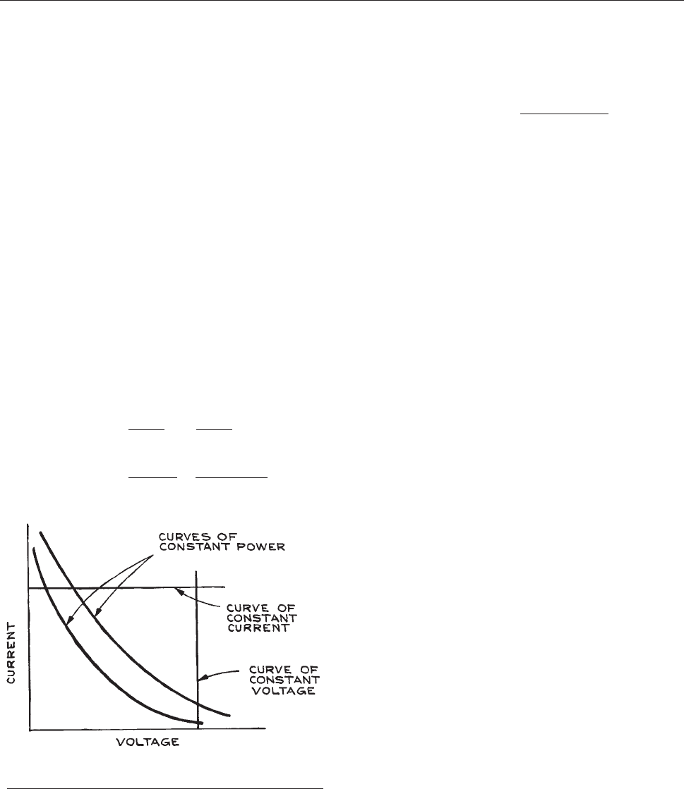
6.5.1 Power-Supply Specifications
Power supplies are specifi ed by the maximum current, max-
imum voltage, and maximum power they can deli v er. It is
not always the case that maximum current can be delivered
ov er the complete voltage range of the supply, nor can the
maximum voltage be obtained at all current le v els. This
situation is illustrated in Figure 6.82. Maximum current
can
only be obtained ov er a limited range of voltage without
exceeding the power rating of the supply.
The change in output voltage per unit change in input
a.c. voltage is called the line regulation, while the change
in output voltage per unit change in load or output current
is called the load regulation. Both are generally specified
as a percentage. Many power supplies can be operated in a
constant-current mode where the output is a current essen-
tially independent of input and output voltage. Regulation
specifications then apply to the output current. Load reg-
ulation can be translated into an equivalent dynamic-out-
put resistance, since the relative change in load is the
negative of the relative change in current DR/R ¼DI/I:
load regulation ¼
DV=V
DR=R
¼
DV=V
DI=I
¼
DV=DI
jj
V=I
¼
R
dynamic output
R
load
ð6:47Þ
As an example, if a filament power supply produces 3 A
at 5 V, and the load regulation is 0.1%, then the dynamic
output resistance is:
R
dynamic output
¼
1 3 10
3
3 5V
3A
¼ 1:67 3 10
3
X ð6:48Þ
Transient response and recovery time relate to the ability
of the power supply to recover from sudden changes in
load or line voltage at the stated operating point. If the line
and load fluctuations are rapid, the power-supply regulat-
ing circuits may not be able to keep up with them and the
resulting regulation will be considerably worse than speci-
fied. Generally, the better the regulation, the slower the
response to changes of line and load conditions. The reg-
ulation may also depend on the output power level, a point
worth noting in the specifications.
As well as maintaining a constant average d.c. leve l,
instantaneous values of the output voltage should not deviate
appreciably from the av erage. De viations come from ripple
at twice the line frequency for dissipati v e regulators, at the
switching frequency for switching regulators, and from reg-
ulating circuit transients. Specificati on of the rms ripple gi v es
an indication of the effecti v eness of the filter ing circuits. It
giv es no indication, howev er, of the presence of short-dura-
tion, large-amplitude voltage spikes at the output. A maxi-
mum peak-to-peak noise specification is used to describe this
kind of instantaneous voltage deviation. As with regulation,
ripple and noise may depend upon the power level.
Even with a constant line voltage and constant load, the
output voltage can change if the temperature changes. This is
generally indicated by a temperatur e-coeffi cient specification,
which gives the percentage change in output voltage per
degree change in temperature about a specified temperature.
For laboratory applications, this is usually not a critical spec-
ification. When working in extreme environments, howev er,
it may be significant (for compact units that depend on
forced-air cooling or free-con vection cooling, adequate space
must be provided in the mounting to pre vent overheating).
Power supplies that convert a d.c. input voltage to a dif-
ferent d.c. output voltage are particularly useful when d.c.
rather than a.c. voltages are available. Voltage conversion
with these supplies is accomplished by changing the d.c.
input to a.c. at frequencies of 20 kHz and above, changing
Figure 6.82 Current, voltage, and power relations for a
power supply.
442 ELECTRONICS
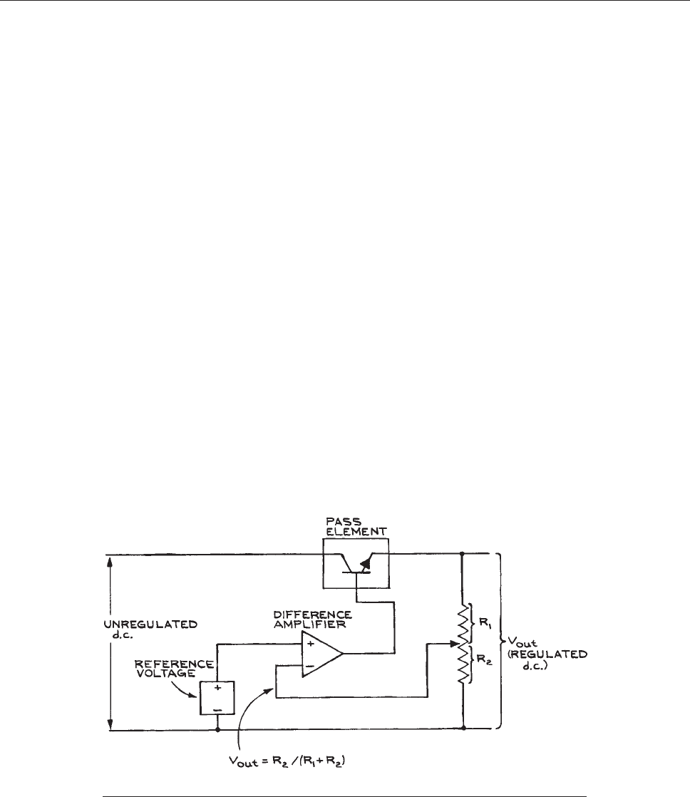
the amplitude of the high-frequency a.c. with a transformer,
and rectifying and regulating the output of the transformer.
The ratio of the maximum output power to maximum input
power is the efficiency of conversion. d.c. to d.c. converters
have efficiencies that exceed 70 to 80% and are available in
a wide range of input and output voltages and powers. When
high voltage at low current is required, as, for example, for a
photomultiplier tube or electron multiplier, these units are
particularly convenient.
Though often not included in the specification list, radio
frequency (rf) noi se can be an important consideration for
supplies used in the vicinity of sensitiv e wide-band ampli-
fiers and when trying to extract a weak signal from noise.
Some types of power supplies produce more r.f. noise than
others because of the design of the regulating circuit. Switch-
ing regulators with SCRs are particularly poor in this regard.
Other factors to consider in a power supply are bipolar
operation (can both the negative and positive terminals be
grounded to give positive and negative output voltages,
respectively?) and insulation from ground if the supply is
to be floated on another supply. Operation is simplified by
front-panel meters indicating both output voltage and cur-
rent, overload reset switches, and a convenient output ter-
minal configuration and location.
A single output power supply can never be used to sup-
ply two voltages, one negative and one positive with
respect to ground. When it is necessary to have such vol-
tages as, for example, with operational-amplifiers, two
separate supplies must be used.
6.5.2 Regulator Circuits and Programmable
Power Supplies
A block diagram of a dissipative regulator circuit in a
power supply is illustrated in Figure 6.83. The sensing
res
istors R
1
and R
2
are across the output of the power
supply. A fraction R
2
/(R
1
þ R
2
) of the output voltage is
sent to a difference amplifier, where it is compared with a
reference voltage, and the amplified difference used to con-
trol the pass element, a transistor in the common-collector
configuration in this example. Depending on the output of
the difference amplifier, the pass-element output voltage
will adjust itself to a value just sufficient to sustain the
required input from the difference amplifier. If, for some
reason, the output voltage rises, the output of the difference
amplifier will decrease and the pass-element output will
decrease. The opposite occurs for a falling output. The
series dissipative regulator is inefficient because the differ-
ence in voltage between the raw d.c. input and regulated
d.c. output falls across the pass element, which must then
dissipate power equal to the product of this voltage differ-
ence and the output current.
Figure 6.83 Block diagram of the regulator circuit in a power supply.
POWER SUPPLIES 443

More efficient power supplies use circuits to control the
duty cycle of the pass element. In these circuits, the pass
element (a transistor, SCR, power MOSFET, IGBT, or
other solid-state device) acts as a switch and is either on
(no voltage drop across it) or off (no current through it).
The output voltage from such a regulator is:
V
out
¼ V
in
t
on
t
on
þ t
off
ð6:49Þ
where t
on
is the time for which the pass element is on and
t
off
is the time for which it is off in each cycle. The optimum
switching frequency for switching regulators is between 20
and 100 kHz. At these high frequencies, r.f.i. is present and
can cause problems with sensitive electronic circuits.
In practice, regulator circuits can be very complex, with
high-gain difference amplifiers or comparator preregulators,
multiple pass elements, overload and overvoltage protec-
tion, and temperature compensation. The above general
power-supply description, however, is sufficient for an
understanding of remote programmable power supplies. If
R
1
and R
2
in Figure 6.83 are replaced by a potentiometer, a
change in its setting will result in a change in the regulated
output voltage. This is what occurs when one changes the
dial settings on the front panel of a variable power supply.
The internal potentiometer can clearly be replaced by an
external potentiometer (resistance programming) – or even
more directly – by an external voltage source (voltage pro-
gramming). The addition of such features requires very little
modification to the basic power-supply regulator circuit, and
they are often available at no cost or as low-cost options.
Remote programming can be particularly useful in control
operations, where a digital code from a computer is changed
to a voltage by a digital-to-analog converter (DAC), and this
voltage is used to set the output of a power supply.
Overvoltage protection is an important feature in a
power supply. With such protection, one is assured that
no failure will result in a high voltage across the output
terminals of the supply. Crowbar circuits using SCR
switches are often used for overvoltage protection. Such
circuits short the output terminals of the supply when the
output voltage exceeds a preset value. The resulting short-
circuit current causes a fuse to blow or a circuit breaker to
open, shutting down the power supply until the fault that
caused the overvoltage is corrected. It is essential that the
protection circuit responds quickly to overload conditions
to avoid damage to the power supply. Response speed
should be included in the specifications.
Another built-in safety feature found on power supplies is
foldback current limiting. When the output current exceeds
a specified limit, it is automatically reduced by such circuits
to a low level and maintained there for a specified time
before being reset. Current-limiting circuits are triggered
by temperature-sensitive or power-dissipating elements.
In addition to variable output power supplies there are a
large number of fixed-voltage power supplies on the market.
When working with logic circuits and operational amplifier
circuits, only fixed power-supply voltages are required.
Most fixed-voltage supplies inc orporated in other units are
designed to operate from the a.c. line, although there are a
number of a.c.-to-d.c. converters. The least expensiv e config-
uration is the card power supply [Figure 6.84(a)]. All com-
po
nents are on a single printed circuit board with edge
contacts. The a.c. input must be brought to one set of contacts
and the d.c. output taken from another. For routine use, the
card supply should be mounted in a case or on a rack panel
with an on–off switch, a pilot light, a fuse, and output termi-
nals. This requires additional time and expense, which may
cancel the initial cost savings from purchasing such a supply.
Frame-mounted supplies [see Figure 6.84(b)] are similar
to
the card supplies in that all external connections,
switches, and output terminals are missing. The metal frame
facilitates mounting, however, and affords some protection
to the components. Rather than PCB contacts, frame sup-
plies usually have screw-type barrier connectors.
Fixed-voltage supplies also come in enclosed cases and
in encapsulated units suitable for direct connection to a
printed circuit board [see Figure 6.84(c)]. Many of the
so-called
fixed-voltage supplies can be adjusted over a
5–10 % range about the nominal output voltage value.
Multiple fixed-voltage units with two and even three vol-
tages are also common. It is often useful to have 615 V
and þ5 V available from a single power supply when both
linear and digital circuits are used together.
Manufacturers produce a wide range of supplies with dif-
ferent voltages, power ratings, and mechanical configura-
tions. It is therefore rarely worthwhile to construct a po wer
supply. A possible exception lies in the use of integrated-
circuit modules. There are two general types: fixed and
variable output. The fixed-output units are three-terminal
devices – unre gulated d.c. is applied across the input and
444 ELECTRONICS
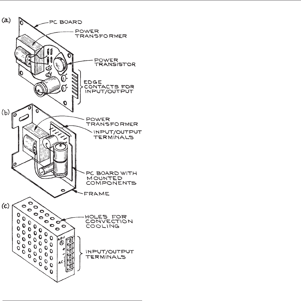
common terminals, and regulated d.c. at the appropriate
voltage appears between the output and common terminals.
A representativ e unit of this type is the LM109 5 V, 1.5 A
monolithic regulator . The regulator combines on-chip thermal
shutdown with current limiting, an on-chip series pass
transistor, and a stable internal voltage reference. Further
details about the LM109 and its use in other applications
are available from the manufacturer.
6
The LM105 is an example of a variable-voltage integrated-
circuit re gulator. For this unit, the output is set by the ratio of
two external resistances. The maximum output voltage is
40 V, and the maximum output current is 20 mA. When an
external pass transistor is added to the basic regulator circuit,
the load current can be increased to 500 mA. The LM105 can
also be used as a switching regulator. Data and application
sheets should be consulted when using such regulators.
Useful power-supply circuits with integrated regulators
are illustrated in Figure 6.85. Fixed-voltage units are made
by
several manufacturers at several fixed voltages from 4
to 20 V. Variable units are available for both positive and
negative voltages.
Though not strictly po wer supplies, integrated-circuit volt-
age references provide precise output voltages for d.c. input
voltages that can span a relati v ely wide range. Output vol-
tages are from 1 to 10 V with initial accuracies from 0.01 to
1.2%. Change in output voltage with temperature for these
units varies between 1 and 50 parts per million per degree
Celsius (ppm/°C). Output noise is exceptionally low, varying
from 1 to 50 lV peak-to-peak over a bandwidth of 0.1 to 10
Hz. Output currents are low, 5 to 100 mA.
6.5.3 Bridges
Bridges are used to measure the electrical properties of a
circuit element by comparison with a similar element. The
Wheatstone bridge, dev eloped in the early nineteenth century,
compares the potentials from two voltage di viders connected
in parallel across a voltage source, as shown in Figure 6.86(a).
T
aking the difference between the potentials at the
junction of R
1
and R
2
and R
3
and R
4
, V
out
¼ V
in
R
3
=½
ðR
1
þ R
3
ÞR
4
=ðR
2
þ R
4
Þ. When V
out
¼ 0, R
1
=R
2
¼
R
3
=R
4
, the null condition. In the standard configuration,
R
1
and R
2
are fixed, R
4
is the resistance to be measured,
and R
3
is v a ried until a null or balanc e condition is achiev ed.
At null the relation between the resistances is independent of
V
in
. Null-type measurements require a means for v arying one
element of the bridge, and this is usually accomplished with a
system that incorporates feedback.
Bridges in most transducer applications are operated
off-null, or out of balance. For the simple bridge in Figure
Figure 6.84 Fixed-voltage power supplies; (a) card supply;
(b) frame supply; (c) enclosed case.
POWER SUPPLIES 445

6.86(b), three of the resistors are fixed at value R while the
one to be measured, R
x
, deviates from R by xR, where x is a
unitless variable. The output voltage V
out
is given by:
V
out
¼ V
in
R
2R
R
x
R þ R
x
¼
V
in
4
x
1 þ x=2
ð6:50Þ
For x=2<<1; V
out
V
in
ðx=4Þ.Asanexample,let
x ¼0.01, then V
out
¼V
in
ð0:01=4Þ, so that a 1% change
in R
x
gives a 0. 25% change in V
out
. The sensitivity of
the bridge, defined as the change in output voltage for
a given change in input voltage, is 250 mV/V. Bridge
sensitivity can be doubled by adding a second identical
variable element opposite the first, as shown in Figure
6.8
6(c). While the output of such a configuration is
doubled,
the nonlinearity remains. The addition of two
more variable elements, R
C
¼ R(1 – x), with resistances
that change in opposite ways to the original elements,
results in a bridge with output equal to the fractional
change in resistance times the reference voltage. This is
shown in Figure 6.86(d). Bridges of this type are used with
two-element
strain gauges and piezo-resistive transducers.
The transducers are arranged so that there are complemen-
tary changes in resistance for sensors in adjacent bridge
arms.
Another way to linearize the output of a bridge circuit is
by inserting an operational amplifier to null the bridge by
adding a voltage in series with the variable element R
x
that
is equal in magnitude and opposite in sign to the incre-
mental voltage across R
x
. This gives an output that is linear
in x for large values of x.
In bridge circuits that are operated out of balance, the
output is proportional to the reference voltage V
in
. A stable
reference voltage can be derived from an IC reference
source followed by an operational amplifier stage. Ana-
log Devices and Maxim Integrated Products manufacture
signal-conditioning power supplies that have program-
mable outputs and include amplification and filtering. Be-
cause neither side of the bridge from which the voltage is
measured is at ground, instrumentation amplifiers are the
preferred devices for reading bridge outputs. These ampli-
fiers have the necessary differential inputs, high common-
mode rejection ratios, high input impedances, and resist-
ance programmable gain.
Figure 6.85 Examples of circuits with the LM109 fixed-
voltage regulator and the LM105
variable-voltage regulator.
446 ELECTRONICS
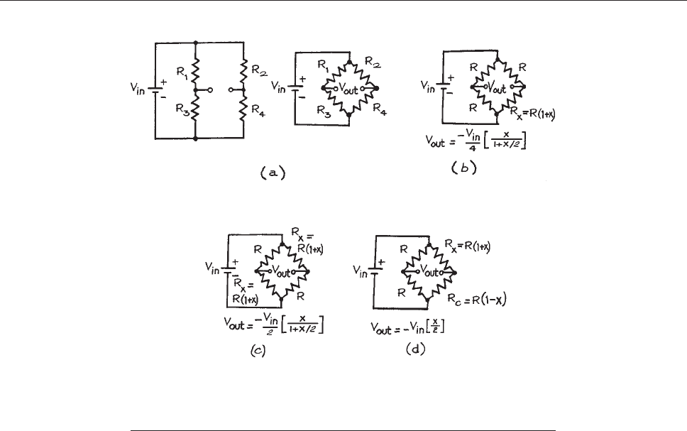
6.6 DIGITAL ELECTRONICS
Digital systems are based on circuit elements (usually tran-
sistors) operated in such a way that they exist in only one
of two states. This is in contrast to analog systems, where
the outputs are continuous functions of the input variables.
Combinations of two-state, or binary, devices can perform
arithmetic and logic operations of arbitrary degrees of
complexity.
6.6.1 Binary Counting
With a binary system, it is usual to call the states 0 and 1.
Combinations of 0s and 1s can then be used for counting.
Some schemes are given in Table 6.26. Note that the lea
st
significant bit (LSB) or column is 2
0
, the next 2
1
, and the
last or most significant bit (MSB) is 2
4
. In other words, the
binary number system is merely a base 2 system, while
the decimal system is base 10. Other systems derived from
the binary system are the octal (base 8) and the hexadeci-
mal (base 16), as detailed in Table 6.26. In the binary
sys
tem, the number 2 does not appear, and in the octal
system 8 does not appear. The hexadecimal system substi-
tutes the letters A, B, C, D, E, and F for the decimal num-
bers 10, 11, 12, 13, 14, and 15, for which a single symbol
does not exist.
The state of the output of a logic device can be represented
by a voltage le v el or the presence or absence of a signal pulse
within a gi v en time window. A voltage-level system in which
the most positive voltage le v el corresponds to logical 1 is a
positive-logic system. One in which the least positi ve level
corresponds to logical 1 is a negative-logic system.
6.6.2 Elementary Functions
The basic logic gates, along with the corresponding rela-
tionships between input and output variables, are given in
Table 6.27 in truth-table form
along with the schematic
symbols.
Figure 6.86 (a) Wheatstone bridge; (b) off-null bridge with one variable
element; (b) off-null bridge with two variable elements; (c) off-null bridge with
two compensating variable elements; (d) off-null bridge with a compensati ng
variable element.
DIGITAL ELECTRONICS 447

6.6.3 Boolean Algebra
The rules for manipulating logic expressions based on
binary logic were formulated in the nineteenth century by
George Boole. The laws and identities are given in Table
6.2
8. Boolean algebra is useful for reducing complex truth
ta
bles to the fewest possible gates. Consider, for example,
the three-variable (A, B, C), two-function (X, Y) truth table
at the top of Figure 6.87. The Boolean algebra expressions
fo
r X and Y are obtained by identifying the states of each of
the variables (A, B, C) for which the function under con-
sideration (X or Y) is in the 1 state. For example, X ¼ 1
when A ¼ 0, B ¼ 0, and C ¼ 1. By convention, a bar over a
variable symbol indicates negation, so that if A ¼ 0,
A ¼ 1.
The coincidence of 1s at
A,
B,andC to give X ¼ 1 requires
an AND operation, which is the first term in the full expres-
sion for X in Figure 6.87. The other terms are derived from
th
e truth table in the same way, and they are all connected
together by OR operations. After simplification by applica-
tion of the laws in Table 6.28, the expressions can be imple-
me
nted with elementary gates. The gates for the function X
are shown at the bottom of Figure 6.87.
Another
way of simplifying truth tables is by making a
logic map called a Karnaugh map. The map for the truth
table of Figure 6.87 is shown in Figure 6.88. The squares
corresponding
to the variables for which X and Y are 1 are
shaded. Contiguous shaded squares corresponding to 0 and
1 for a single variable, say C, with the other variables
constant, show that the value of the function is independent
of the state of C. In the map for Y, it can be seen that the
squares for
A B are shaded for C and
C. It therefore fol-
lows that the state of Y is not dependent on the variable C
for these cases.
6.6.4 Arithmetic Units
After elementary gates, the next simplest logic units are
those that perform elementary binary arithmetic operations.
Some common arithmetic units are gi v en in Table 6.29.The
truth
table for the half adder follows the rules for binary
addition with C the low-order bit of the sum and D the
high-order bit. The full adder is an elaboration of the half
adder with an extra input. When adding two binary numbers
of more than one bit each, provision must be made for the
carry operation. This is the function of the C
n1
terminal,
that accepts the carry bit from the result of adding the pre-
ceding lower -order bits in the string (thus the designation
C
n1
). The results from the addition of the n-order bits
appear at terminals C
n
and S
n
.Thedigital comparator com-
pares the magnitude of the digital signals at input A
n
and B
n
and activates output C
n
, D
n
,orE
n
depending on whether A
n
>
B
n
, A
n
< B
n
,orA
n
¼ B
n
. Such elements can be connected
together to compare two n-bit binary numbers. The parity of
a binary number is defined as odd (0) if there is an even
number of ls and ev en (1) if there is an odd number of 1s.
The parity code is often used to check for transmission errors
in bit strings. By sending a parity bit with an n-bit word
and testing the receiv ed word against the parity bit, single
bit errors can be detected. This is illustrated for a four-bit
word with the parity generator/chec ker in Table 6.29.
6.6.5 Data Units
For data acquisition and transmission, decoders, encoders,
multiplexers, and demultiplexers are commonly used. The
read-only memory (ROM) is a combination of decoder and
Table 6.26 Systems of numeration
Decimal Binary Octal Hexadecimal
0 0000 00 0
1 0001 01 1
2 0010 02 2
3 0011 03 3
4 0100 04 4
5 0101 05 5
6 0110 06 6
7 0111 07 7
8 1000 10 8
9 1001 11 9
10 1010 12 A
11 1011 13 B
12 1100 14 C
13 1101 15 D
14 1110 16 E
15
/
MSB
1111
)
LSB
17 F
448 ELECTRONICS
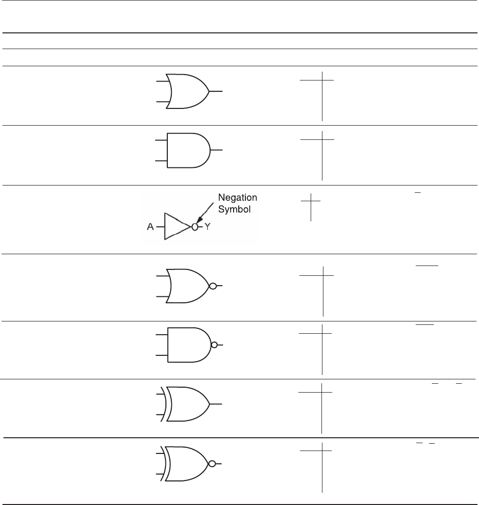
Table 6.27 Logic gates
Name Symbol Truth Table Boolean Expression
OR
A
B
Y
ABY Y¼A+B
000
011
101
111
AND (coincidence)
A
B
Y
ABY Y¼A B
000
010
100
111
NOT (inverter)
AY
Y ¼
A
01
10
NOR
A
B
Y
ABY Y¼A þ B
001
010
100
110
NAND
A
B
Y
ABY Y¼A B
001
011
101
110
XOR (exclusive OR,
anticoincidence)
A
B
Y
ABY Y¼ðB AÞþðB AÞ
000
011
101
110
XNOR (exclusive, NOR,
equivalence)
A
B
Y
ABY Y¼ A B þ A B
001
010
100
111
DIGITAL ELECTRONICS 449
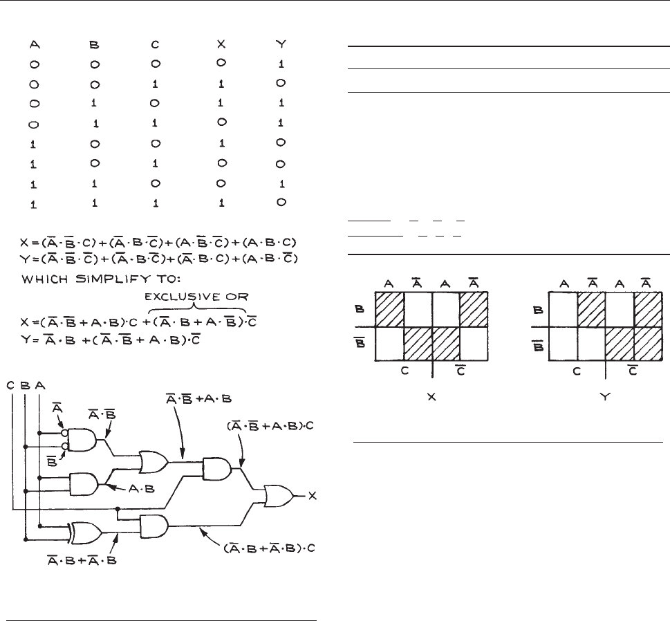
encoder and is frequently used to implement complex truth
tables. Programmable and erasable ROMs, called PROMs
and EPROMs, can have their internal logic modified for
the particular application of the user. Table 6.30 gives the
truth
tables and input–output terminal arrangements for
some simple data units.
6.6.6 Dynamic Systems
The logic units described so far are considered to be static
or combinatorial, because the output levels depend only on
the current input levels. The previous history of the signals
at the different inputs is irrelevant. With dynamic or
sequential systems, output signal levels depend on the his-
tory of the signal levels at the input terminals. The truth
tables for dynamic systems must specify the previous
states of the inputs and outputs in order for the state of a
particular output to be fully determined. Subscripts are
used to differentiate the time sequence of the output states.
Table 6.31 lists a number of flip-flops that
are the basic
building blocks in dynamic systems. Flip-flops can be
strung together to make shift registers and counters. A shift
register is a series of J/K flip-flops with the Q and
Q outputs
of each stage connected to the J and K inputs of the next
stage (see Figure 6.89). Data are entered serially in the first
Table 6.28 Boolean Algebra
Laws Identities
Commutative A þ A ¼A
A þ B ¼B þ AA A ¼A
A B ¼B AAþ 1 ¼1
A 1 ¼A
Distributive A þ 0 ¼A
A (B þC) ¼A B þA CA 0 ¼0
De Morgan
A B C ¼ A þB þ C
A þ B þC ¼ A B C
Figure 6.87 Example of a truth table, the equivalent
Boolean algebraic expression, and implementation with
elementary gates.
Figure 6.88 Karnaugh map for the truth table of
Figure 6.87.
450 ELECTRONICS
Table 6.29 Arithmetic units
Name Symbol Truth Table
Half adder
AB
CD
HA
A B Sum C D
0000 0 0
0101 0 1
1001 0 1
1110 1 0
Full adder
A
n
B
n
C
n-1
C
n
S
n
FA
A
n
B
n
C
n-1
S
n
(sum) C
n
(carry)
000 0 0
010 1 0
100 1 0
110 0 1
001 1 0
011 0 1
101 0 1
111 1 1
Digital comparator
CD
E
n
C
n
D
n
A
n
B
n
C
n
(A
n
>B
n
)D
n
(B
n
>A
n
)E
n
(A
n
¼B
n
)
000 0 1
010 1 0
101 0 0
110 0 1
Parity generator/checker
ABCD P'
P
A
0
0
0
0
0
0
0
0
1
1
1
1
1
1
1
1
B
0
0
0
0
1
1
1
1
0
0
0
0
1
1
1
1
C
0
0
1
1
0
0
1
1
0
0
1
1
0
0
1
1
D
0
1
0
1
0
1
0
1
0
1
0
1
0
1
0
1
zfflfflfflfflfflfflfflfflfflfflfflfflfflfflfflfflfflfflfflfflfflfflfflfflfflfflffl}|fflfflfflfflfflfflfflfflfflfflfflfflfflfflfflfflfflfflfflfflfflfflfflfflfflfflffl{
4bit word
Parity bit
PðP
0
=1Þ
0
1
1
0
1
0
0
1
1
0
0
1
0
1
1
0
PðP
0
=0Þ
1
0
0
1
0
1
1
0
0
1
1
0
1
0
0
1
DIGITAL ELECTRONICS 451
Table 6.30 Data units
Unit Symbol Truth Table
Decoder: Activates
one of 2
n
outputs
according to
an n-bit code.
CB A
X
0
X
1
X
2
X
3
X
4
X
5
X
6
X
7
CBAX
0
X
1
X
2
X
3
X
4
X
5
X
6
X
7
0 0 0100 0000 0
0 0 1010 0000 0
0 1 0001 0000 0
0 1 1000 1000 0
1 0 0000 0100 0
1 0 1000 0010 0
1 1 0000 0001 0
1 1 1000 0000 1
Encoder: n-bit
output code for
activation of one of
2
n
input lines.
0
1
2
3
4
5
6
7
8
9
DCBA
2
3
2
2
2
1
2
0
Input D C B A
00000
10001
20010
30011
40100
50101
60110
70111
81000
91001
Multiplexer: According
to an n-bit code, one
of 2
n
signal input lines
is connected to a
single output line.
8-to-1 line multiplexer
shown.
B
2
B
1
B
0
A
0
A
1
A
2
A
3
A
4
A
5
A
6
A
7
MUX
Y
B
2
B
1
B
0
Y
000A
0
001A
1
010A
2
011A
3
100A
4
101A
5
110A
6
111A
7
452 ELECTRONICS
unit, connected as a D flip-flop, and move from unit to unit
at each clock transition. Shift registers can be used as
counters, serial-to-parallel data converters using the paral-
lel outputs, and parallel-to-serial data converters using the
parallel inputs.
The basic serial or ripple binary counter is shown in
Figure 6.90. Three J/K flip-flops
can count to 2
3
in this
arrangement. In the shift-register configuration, eight flip-
flops are needed to count to 2
3
.
Modulo-N counters with N 6¼ 2. These counters can be
made by decoding the counter outputs with gates and reset-
ting the flip-flops after N counts. Shift registers and coun-
ters are manufactured in a variety of configurations in
single 14- and 16-pin DIP and SMT packages.
6.6.7 Digital-to-Analog Conversion
Whenever it is necessary to connect a digital system to
an external device that operates in an analog mode, con-
verters are needed – either digital-to-analog (DAC) or
analog-to-digital (ADC). Of the two, the DAC is the
more fundamental, since many ADCs use DACs in their
construction.
A DAC produces an output current or voltage propor-
tional to the magnitude of the binary number at its input
terminals (see Figure 6.91). In one design, the binary
in
puts to a DAC activate FET analog switches that con-
nect the properly weighted current or voltage from a
reference source to the output. In the case of voltage
Table 6.30 (cont.)
Unit Symbol Truth Table
Demultiplexer: According
to an n-bit code, a single
input line is routed to
one of 2
n
output lines.
C B A Y Connected to
000X
0
001X
1
010X
2
011X
3
100X
4
101X
5
110X
6
111X
7
Read-only memory (ROM):
Combination of a
decoder and encoder
to convert an n-bit code
to an m-bit code, where
n and m are not
necessarily equal. 3-bit
input code (A
1
,B
1
,C
1
)
and 4-bit output code
(A
2
,B
2
,C
2
,D
2
) shown.
A
1
B
1
C
1
D
2
C
2
B
2
A
2
DIGITAL ELECTRONICS 453
Table 6.31 Flip-Flops
Unit Symbol Truth Table
R/S (reset-set) flip-flop:
Basic digital memory
unit.
R/ S
S
R
Q
Q
SRQQ
0101
1010
0 0 Indeterminate
1 1 Indeterminate
J/K flip-flop:An
elaboration
of the R/S avoiding
the indeterminate 1, 1
and 0, 0 states,
with separate preset (Pr)
and clear (Cr) inputs,
and a clock (Ck) input
that must be activated
for the outputs
to follow input
conditions.
J
K
Ck
Q
Cr
Q
J/ K
Pr
Upon the application of a Ck pulse
a
J
n
K
n
Q
n+1
Q
nþ1
00
Q
n
Q
n
0101
1010
11
Q
n
Q
n
Direct inputs
Pr Cr Q
Q
0 0 Disallowed
0110
1001
1 1 Normal Clocked Operation
D (delay) flip-flop: Input
state appears at the
output
after a clock
pulse. Constructed
from a J/K flip-flop with
an inverter from J to K,
signal
applied to J.
J
K
Ck
Q
Q
D
Input
Upon the application of a Ck pulse
Input Q
Q
001
110
T (toggle) flip-flop:
Output changes
state at each
clock transition.
Used as a binary
divider. Constructed
from a J/K flip-flop by
fixing J and K at logic 1.
J
K
Ck
Q
Q
T
1
a
The subscript n + 1 designates the (n + 1)th state as distinct from the previous nth state. When R and S are 0, the output of Q remains
constant, equal to its previous value.
454 ELECTRONICS
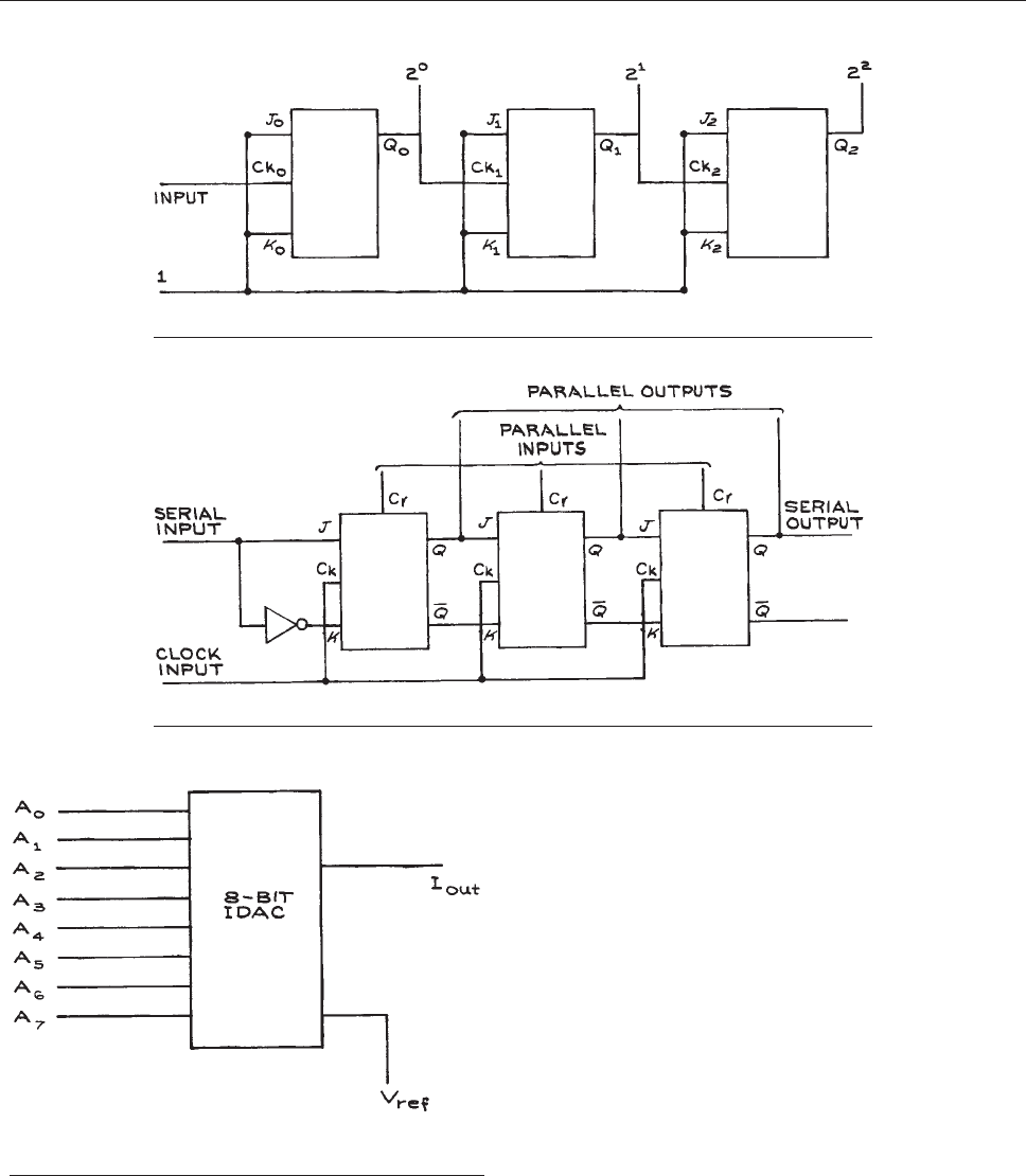
DACs, an operational amplifier in the summing mode
adds the weighted input voltages. Electric al specifications
to consider with a DAC are resolution, the number of
input bits or steps (an 8-bit DAC has 256 steps); linearity,
the maximum deviation from t he best straight line drawn
through the graph of output versus digital input; and
accuracy, the deviation of the output from that computed
on the basis of the digital input. Linearity primarily
depends on the resistors in the DAC circuit and the volt-
age drops across the internal transistor switches. For these
reasons, linearity is temperature dependent. Accuracy
depends on the factors a ffecting linearity and also on
the reference voltage, either inte rnal or extern al. In app li-
cations where speed of conversion is important, settling
time must be considered. This is the time necessary for
the analog output to stabilize to a level th a t is the
Figure 6.89 J/K flip-flops arranged as a 3-bit shift register.
Figure 6.90 J/K flip-flops arranged as an 8-bit binary ripple counter.
Figure 6.91 An 8-bit current digital-to-analog converter
(IDAC).
DIGITAL ELECTRONICS 455
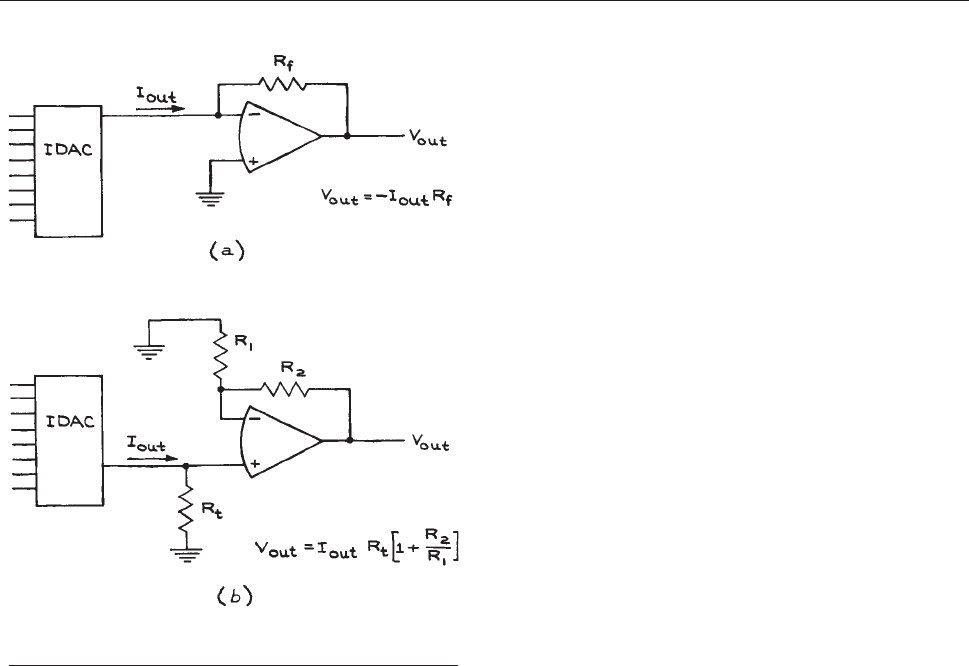
equivalent of 61/2 of the least significant bit of the binary
input. Other considerations are power-s upply sensitivity
and compatibility with input a nd output logic levels. If a
currentDACisusedinanapplication where the output
must be a voltage, a current-to-voltage converter is
needed. For low-voltage applications, this can be a resis-
tor. When higher voltages are required, the operational-
amplifier circuits shown in Figure 6.92 can be used. The
characteristics
of the amplifier should not degrade the
expected performance of the DAC with respect to linearity,
accuracy, and settling time.
A variation of the DAC is the multiplying DAC. Since
the output of a DAC is directly proportional to the binary
input and reference voltage, varying the reference voltage
has the effect of multiplying the output by a constant.
Digitally modulated waveforms can be easily produced
with such devices.
There is a larger variety of ADCs than DACs because
the complexity of analog-to-digital conversion lends itself
to a variety of techniques. Four ADC schemes are shown in
Figure 6.93. With the counter
ADC [see Figure 6.93(a)],
pulses from an oscillator or clock are routed to a counter
through control logic, which is activated by the output of a
comparator. The counter output goes to a DAC, the output
of which is compared to the input signal. When the DAC
output equals the input voltage, the comparator changes
state and disconnects the clock from the counter. The
binary number at the counter outputs is then proportional
to the analog input voltage.
The dual-slope ADC [see Figure 6.93(b)] converts volt-
age
to time by using the input voltage to charge a capa-
citor to a predetermined voltage and then discharging the
capacitor by connecting it to a reference voltage of the
opposite polarity. The input voltage is proportional to
the ratio of the charge to the discharge times, which is
recorded by a counter driven by a clock through control
logic. As long as the capacitor, clock, and reference volt-
age are stable during the conversion interval, the resolution
will depend only on the resolution of the capacitor circuit.
This method is the one most commonly used in digital
multimeters.
The successive-approximation ADC [see Figure 6.93(c)]
works
like the counter ADC except that a logic circuit,
rather than a clock and c ounter, drives the DAC. The logic
circuit starts by activating the most significant bit of the
DAC. If the DAC output is greater than the input, the
logic c ircuit turns the MSB off and the next MSB on,
and the comparison is done again. The process of com-
parison continues to the LSB, after which the conversion
is complete. This method is fast a nd has high resolution.
Resolution, linearity, accuracy, and settling time are
important par ameter s used f or characterizing the opera-
tion of ADCs.
The fastest ADCs are flash c onverters. These use 2
N
comparitors, a voltage divider with N resistors, and a
priority encoder to produce an N-bit binary output. The
speed of conversion depends primarily on the speed of
the comparitors. Eight-bit ADCs that can convert at a
rate of 10
9
samples per second (GSPS) are widely avail-
able. A simple 3-bit flash converter circuit i s shown in
Figure 6.93(d) along with the truth table f or the priority
encoder
.
Figure 6.92 Conversion of the current output of an IDAC
to a voltage output: (a) inverting; (b) noninverting.
456 ELECTRONICS
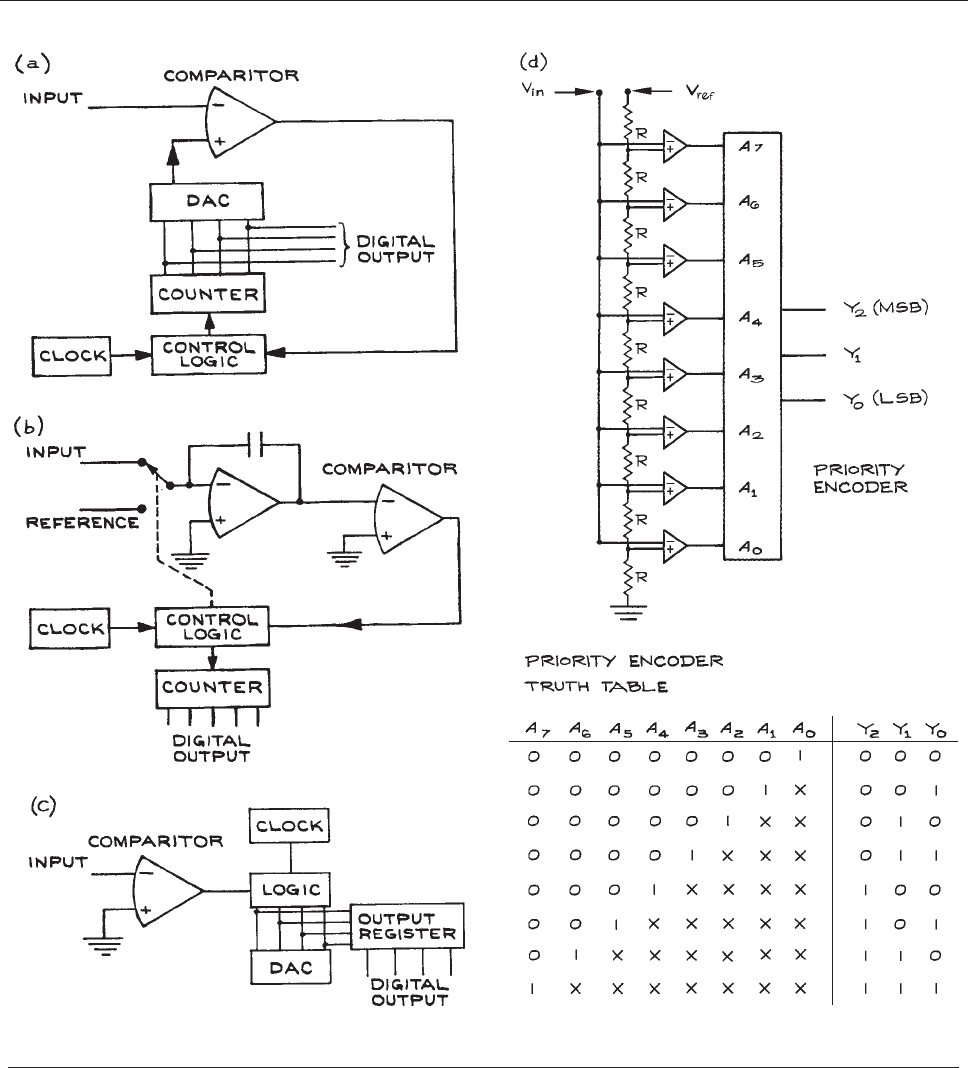
Figure 6.93 Four analog-to-digital converters: (a) counter; (b) dual slope; (c) successive approximation; (d) flash.
DIGITAL ELECTRONICS 457
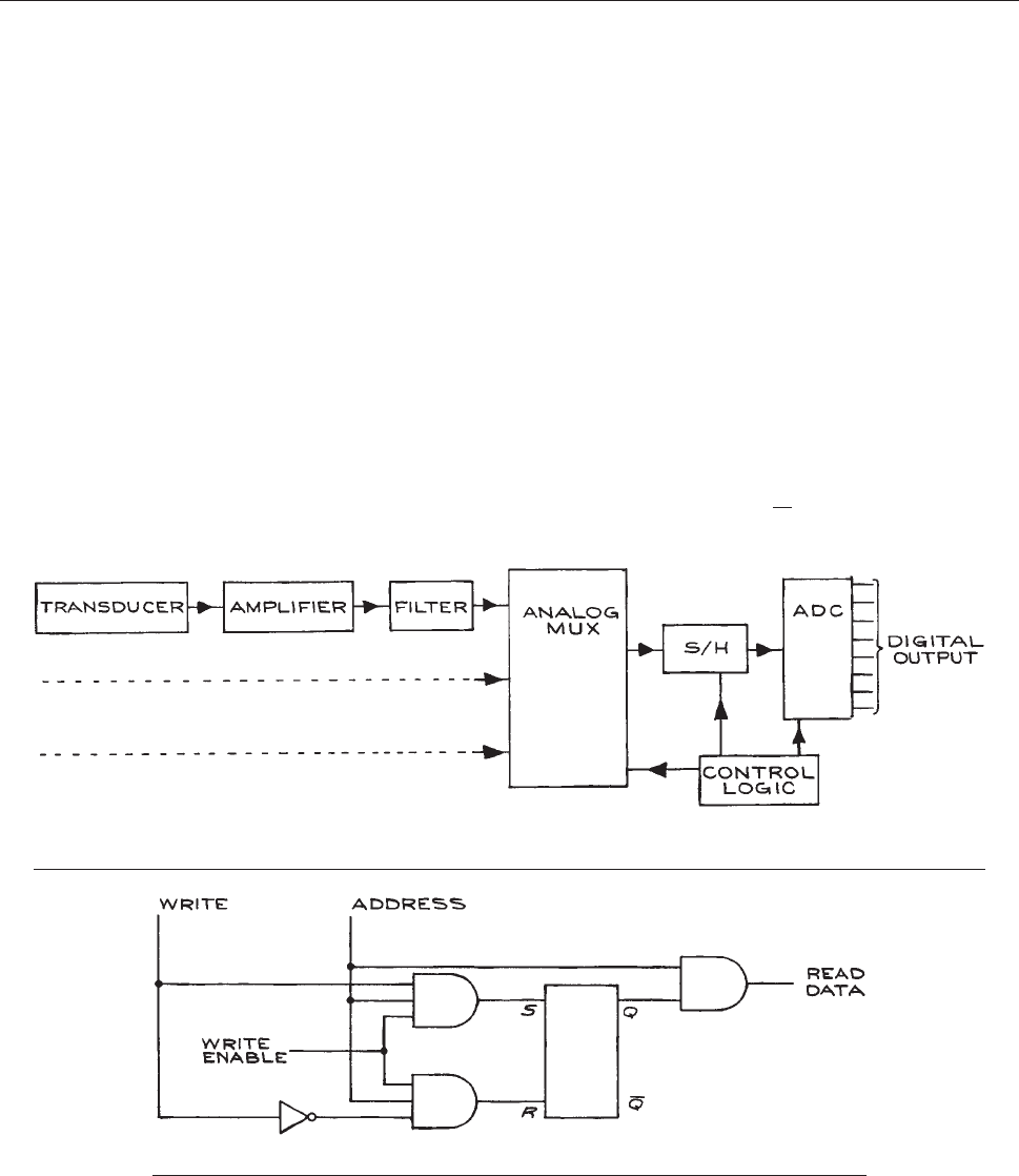
Modular data-acquisition systems or data loggers with an
analog multiplexer (MUX) sample-and-hold (S/H) circuit,
and ADC are av ailable from many sources. A block diagram
of such a system is shown in Figure 6.94. Each of the trans-
ducer
-amplifier-fi lter circuits is connected to the sample-
and-hold circuit for a fixed time thr ough the multiplex er.
The output of the sample-and-hold circuit is then digitally
encoded by the ADC. The frequency at which the various
inputs are sampled depends on the rate at which the signals
are varying. An important theorem of sampling theory states
that if a sampled signal contains no Fourier components of
higher than f
max
, the signal can be recovered with no distor-
tion, if sampled at a frequency of 2 f
max
.
6.6.8 Memories
Large-s cale integration (LSI) and very large-scale inte-
gration (VLSI) have made possible the production of
high-density, solid-state memories. The typical one-bit
memory cell is an R/S flip-flop with supplementary gates,
shown in Figure 6.95. When the ad
dress and write enable
lines are activated, the signal on the write line is registered
on the Q line. It will remain there as long as the write
enable line is not subsequently activated. To read the con-
tents of the memory cell, the address line has only to be
activated. Large-scale memories are composed of billions
of such elementary cells. Because the contents of any
single cell can be read by activating the appropriate
address line, such memories are called random-access
memories (RAMs). There are several different ways of
arranging the basic memory cells for addressing purposes.
For example , a 1024-bit RAM can be arranged as 1024
one-bit words or 256 four-bit words. The addressing
scheme in the first case requires 10 address lines, one data
out line, and one data in line. For the 256 3 4 memory,
eight address lines are needed as well as four data in and
four data out lines. In addition to the address and data
lines, a read/not write (R=
W) line and a chip enable
Figure 6.94 Multiple-input data-acquisition system with an analog multiplexer (MUS), sample-and-hold (S/H) circuit, and
ADC.
Figure 6.95 Basic memory cell.
458 ELECTRONICS

(CE) line are needed. The sta te of the R=W li ne determines
whether data are to be read into or out of the memory; the
CE line is activated when reading or writing data.
Dynamic RAMs require an additional input, called the
refresh, to h old the contents o f the memory. Refreshing
is required continuously with the refresh sign al supplied
from a separate clock. Static RAMs require no such
refreshing. Solid-state RAMs may be volatile, meaning
that their contents are destroyed when the power is inter-
rupted. Battery backup can be provided for these memo-
ries in applications where the memory contents must be
retained in the event of a power failure. For modern mem-
ories based on MOS technology, external power sources
are not necessary to retain memory contents. Examples
are USB memory sticks and fla sh memory cards used in
digital cameras and recorders.
Important parameters to consider for RAMs are power
dissipation, access time, and cycle time. The access time is
the time required after the activation of the address lines to
obtain valid data at the output. The cycle times are the
times required to complete a read- or write-data procedure.
The access and cycle times are related to the power dis-
sipation – generally, the lower the power dissipation, the
slower the memory.
Other considerations are po wer-supply voltages and input
and output signal levels. RAM must be able to accept data
from external devices and, in turn, produce output levels
capable of driving the circuits connected to its outputs.
ROMs are storage devices with permanent, unalterable
patterns of 0s and 1s in the individual cells. ROMs are used
extensively in computers for storage of the character-
generation bit patterns, lookup tables for routine code con-
versions, and control programs, such as those used in cal-
culators.
Programmable read-only memorys (PROMs) are ROMs
whose bit pattern can be altered. They are programmed
with a PROM programmer that permanently burns the
desired bit pattern into the PROM. The bit pattern can be
entered manually (memory location by memory location),
serially, or in blocks under the control of a computer con-
nected to the programmer.
Even more useful devices are erasable PROMS, or
EPROMS. These are programmed in the usual way, but
can also be erased and reprogrammed for other applica-
tions. Erasing is usually accomplished with ultraviolet
light in an EPROM eraser. This can take several minutes.
The EEPROM or electrically erasable PROM, can be very
quickly erased with electrical signals.
An example of the more common series of EPROMs is
the 2700 series, manufactured by INTEL, Advanced Micro
Devices, and others. Members of the series are the 2708,
2716, 2732, 2764, 27128, 27256, and 27512. The digits
following the 27 give the number of kilobits in the
EPROM. For example, the 2732 has 32 kilobits of memory
arranged in a 4096 3 8 pattern – that is, 4 kilobytes. A 12-
bit address (2
12
¼ 4096) is necessary to address 4 kilo-
bytes. The chip also has eight output pins – one pin each
for the þ5 V power, the ground, and the 25 V programming
voltage, and a chip-enable pin. The 2732 chip has 24 pins
and is programmed by entering 0s into the desired memory
locations since all the bits are 1s upon delivery or after
erasure. Programming is accomplished by applying þ25 V
to the OE/VPP programming-voltage pin, while the
address of the byte to be programmed is applied to the
appropriate address pins at the same time that the desired
8-bit pattern is placed on the output pins. When all voltage
levels are stable, a 50 ms TTL low-level pulse is applied to
the CE/PGM chip-enable pin.
Programmers for PROMs are designed to apply the
proper voltages in the required sequence to the PROMs.
Programmers in kit form cost less than $100. Fully
assembled programmers cost from $200 to $500 – the more
costly ones have the capability to program a wide variety of
EPROMs as well as copy and verify EPROM codes. The
programmers generally are controlled through the serial
port of a personal computer, and software is supplied with
the programmer and loaded into the computer. The PROMs
are useful in experimental work because they can be pro-
grammed to reproduce fairly complex truth tables, elimi-
nating the need for several different logic chips. The truth
table of Table 6.34, for example, can be fully implemented
wit
h a PROM having as few as 32 3 4 bits.
The implementation of truth tables with PROMs is inef-
ficient because, in practice, only a limited number of var-
iable combinations are actually used. With a PROM, all
possible combinations of all the input variables are repre-
sented, resulting in a large bit count, most of which is never
used. Programmable array logic (PAL), programmable
logic arrays (PLAs), and field programmable gate arrays
(FPGAs) permit the economical realization of logic
DIGITAL ELECTRONICS 459

expressions with a limited number of inputs and terms. The
units perform the functions of a custom IC. Of the three
devices, the PLAs and FPGAs are the most flexible. Pro-
grammers for these devices are more complicated than
PROM programmers and cost, with software, several hun-
dred dollars for professional models and a few hundred
dollars for student models. XILINX, Altera, and Actel
are manufacturers of programmable logic devices. Cur-
rently FPGAs with as many as 10
6
gates are available for
a few tens of dollars. The two most used languages for
programming FPGAs are VHDL and Verilog. The acronym
VHDL stands for VHSIC Hardware Description Language,
and VHSIC refers to the Very High Speed Integrated Cir-
cuit program originally sponsored by the Department of
Defense for the development of high-speed integrated cir-
cuits. A working knowledge of VHDL is beyond the scope
of the average scientist, however it is quite practical to
implement rather complex codes using the very large vari-
ety of VHDL templates supplied by the manufacturers of
FPGAs. The software necessary to implement VHDL codes
is supplied by the manufacturer of the FPGAs and includes
all steps including logic checking and simulation for imple-
menting the code on an FPGA device. Communication with
the FPGA is through a USB link to a PC.
6.6.9 Logic and Function
To illustrate the ideas in the preceding sections on digital
logic, we now discuss a method for designing an interlock
circuit for a vacuum system.
High-vacuum systems often have a vacuum chamber
connected to a turbomolecular pump through a gate valve
(see Section 3.6.1). The turbo-pump has a high-pressure
outlet
connected to a mechanical rotary pump or dia-
phragm pump via a foreline and foreline valve. A bypass
roughing line with a roughing valve may be used for pre-
liminary evacuation of the chamber. Before this is done,
however, the foreline valve is closed. When the pressure in
the chamber is sufficiently low, the roughing line is closed,
the foreline valve is opened, and the chamber is turbo-
pumped through the gate valve.
To guard against accidents, it is worthwhile to have a
system of interlocks that activates valves in the proper se-
quence and turns the turbo-pump off in case of an accident.
The interlock system consists of sensors that continuously
sample the variables in the v acuum system, such as cooling-
water temperature, cooling-water pressure, foreline pressure,
vacuum-chamber pressure, and roughing-line pressure. The
security of the system depends on whether the physical
property sampled is above or below a predetermined thresh-
old. The second section of the interlock system is the logic,
which, with combinations of elementary gates, establishes
the relationships between the input variables from the sen-
sors and the output functions that control the various vac-
uum-system operations – such as the opening and closing of
the various valves and the application of voltage to the turbo-
pump. Because the output functions only assume one of two
values, the interlock system can be analyzed using either
Boolean algebra or Karnaugh maps. Examples of increasing
complexity are given below. A way of implementing the
system with a data selector is also discussed.
The simplest practical interlock system monitors the
cooling-water temperature and pressure, and turns off the
voltage to the turbo-pump if the water temperature is too
high, the water pressure is too low, or both. A truth table
relating the variables to the function is shown in Table
6.32. The letters and numbers in parentheses are logic
symbols
assigned to the variables (A, B), function (X),
and states of the variables (0, 1). The Boolean logic expres-
sion for the truth table is:
X ¼
A
B ¼
A þ B ð6:51Þ
This is obtained by noting the condition under which
X is in the logical 1 state. Had there been more than one
occurrence of 1 for X, the expression would have
additional OR terms. The Boolean expression can be
implemented with the inverter-and-gate arrangement of
Table 6.32 Truth table
Variables Function
Water
Pressure (A)
Water Temperature (B) Diffusion Pump
Heater (X)
Low (1) Low (0) Off (0)
Low (1) High (1) Off (0)
High (0) Low (0) On (1)
High (0) High (1) Off (0)
460 ELECTRONICS
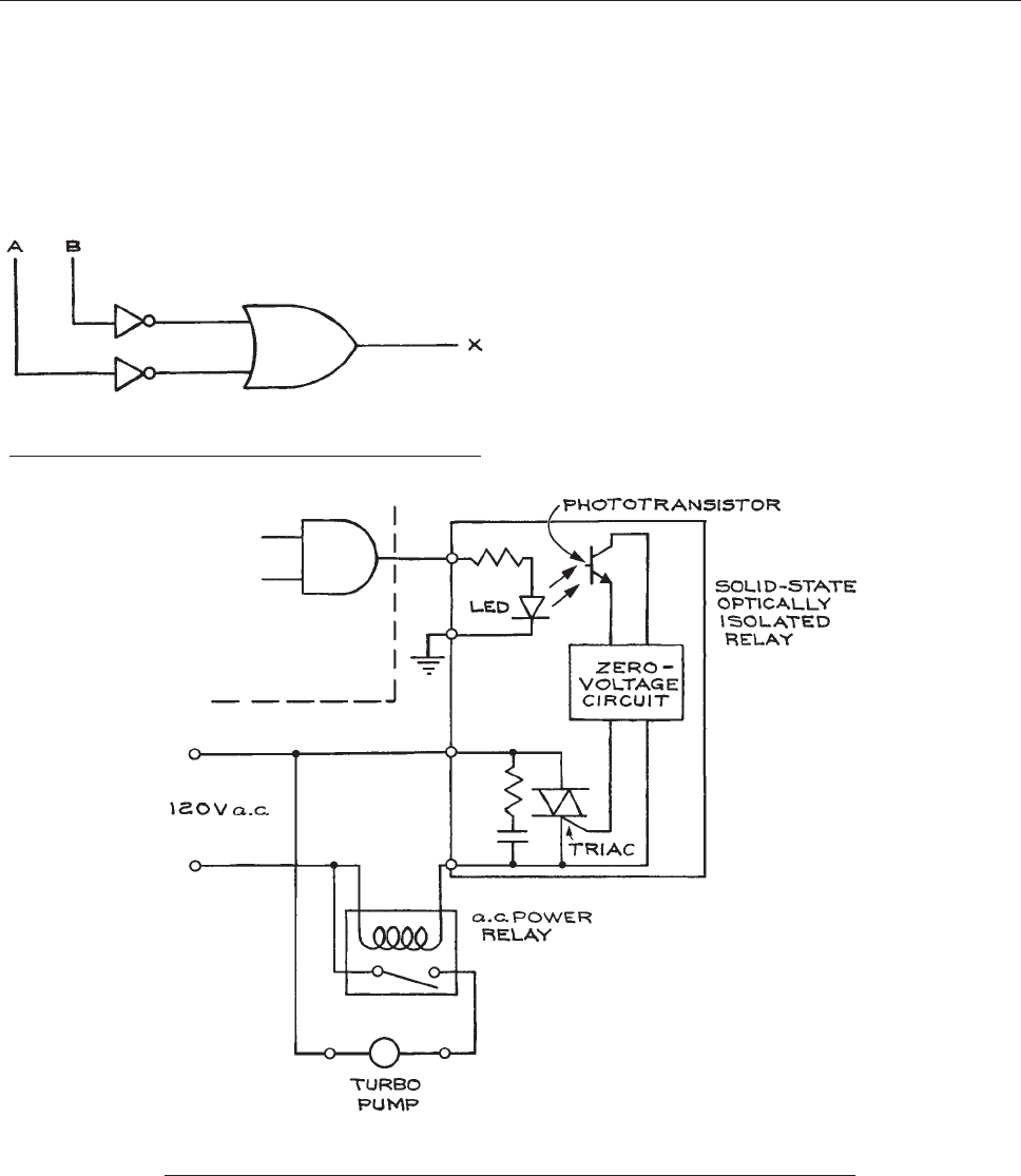
Figure 6.96. A bimetallic-switch temperature sensor can
provide the water-temperature variable, and a diaphragm-
type pressure sensor can provide the water-pressure varia-
ble. Power to the turbo-pump is controlled by a heavy-duty
relay actuated by a solid-state, optically isolated relay
driven by the output of the logic circuit. A practical circuit
is shown in Figure 6.97. It is assumed that logical 0 is less
than
0.8 V and logical 1 is greater than 2.4 V, consistent
with TTL logic. Optical isolators provide an effective inter-
face when controlling power circuits from logic circuits.
An optical isolator contains both an infrared-emitting
diode and a photodetector arranged in a single package,
so that the light from the diode is efficiently transmitted to
the detector through a transparent dielectric medium that
provides electrical isolation. The diode–detector pair is
shielded from ambient light by opaque encapsulating
material. Since only infrared radiation is used to commu-
nicate between diode and detector, there is no electrical
connection between the two. The communication is also
unidirectional, because the detector cannot provide a sig-
nal that can couple back to the diode. Typical applications
for isolators are elimination of common mode input signals
Figure 6.96 Gate arrangement corresponding to
Table 6.32.
Figure 6.97 Practical circuit for a vacuum-system interlock according to the truth table
of Table 6.29.
DIGITAL ELECTRONICS 461
and ground loops, level shifting between two circuits, logic
control of power circuits, and isolation of logic circuits
from noise. The last application commonly occurs when
using the output logic levels on a computer to control
external devices. Infrared-emitting diodes and photodetec-
tors are inherently nonlinear devices, but some isolators
are specially made for linear analog circuits. Photodiodes,
phototransistors, photo-Darlington transistor pairs, and
phototriacs are the detector units in isolators. Important
parameters to consider when choosing an isolator are the
isolation voltage, ratio of output current to light-emitting-
diode input current, and output power-handling capabil-
ities. Trans istor isolators have transfer ratios from 2 to
over 50%, while the Darlington transistor pairs have
ratios from 50 to 500 %. Iso lat ors wi th triac outputs
require i np ut trigger currents in the 10 to 30 mA ra nge
in order to switch 120 V a .c. at curre nts up to a few hun-
dred milliamperes. This is sufficient to drive high-power
triacs, solenoids, small motors, and mechanical relays.
For proper isolator operation, the c haracteristics of the
output stage must be matched to the load. Data sheets
should be consulted. A common package for low-power
isolatorsisasix-pinDIP.
When switching transformer loads, solenoid valves,
contactors, lamp loads, and heaters, output current rating
should exceed the load rating by at least a factor of two.
Solid-state relays provide isolation, and an important
application of solid-state relays is the interface between
computers and power devices. OPTO 22 makes a line of
solid-state relays that can be turned on and off with stand-
ard TTL signal levels. The 120D10 can be used to switch up
to 10 A of a.c. current at 120 V, with a maximum voltage
drop of 1.6 V. The control circuit and switching circuits are
electrically isolated from each other up to 4 kV, and switch-
ing of the load occurs at zero voltage in the a.c. cycle,
thereby eliminating switching transients. Because of the iso-
lation between control signal and load, the circuit supplying
the control signal is protected from voltage spikes. The
relays are 1.2 in. high, 2.4 in. long and 1.8 in. wide.
A more useful interlock system using three variables and
two functions has the truth table of Table 6.33. The vari-
ables
monitored are water pressure and temperature and
turbo-pump foreline pressure. The functions are the turbo-
pump (on or off) and the gate valve (open or closed). The
Boolean expression is also given in the table, while the
Karnaugh map is shown in Figure 6.98 . In the map for Y,
the
1s are adjacent in the 10 column, so that Y is independ-
ent of the state of C.
As a final example of logic design, consider incr easing
the number o f variables to five by includi ng the rough-
ing-line pressure and chambe r pre ssure and a dding the
roughing valve and foreline valve to the functions. With
five variables there will be 2
5
(or 32) combinations.
Table 6.33 Three-variable, two-function interlock
Truth Table
Variables Functions
Water
Pressure
(A)
Water
Temperature
(B)
Foreline
Pressure
(C)
Turbo-
Pump
(X)
Gate
Valve
(Y)
low (0) low (0) low (0) off (0) closed (0)
low (0) low (0) high (1) off (0) closed (0)
low (0) high (1) low (0) off (0) closed (0)
low (0) high (1) high (1) off (0) closed (0)
high (1) low (0) low (0) on (1) open (1)
high (1) low (0) high (1) off (0) open (1)
high (1) high (1) low (0) off (0) closed (0)
high (1) high (1) high (1) off (0) closed (0)
Boolean Expressions
X ¼ A
B C
Y ¼ A
B C þ A B C
Y ¼ A
BðC þ CÞ
Y ¼ A
B
Figure 6.98 Karnaugh map for the truth table of
Table 6.33.
462 ELECTRONICS

Systematic design of the interlock circuit will ensure that
none of them is left out. The truth table is given in Table
6.
34. As an alternative to the Boolean expressions for
the
truth table o r a map, we can use a data selector to
establish the relationships among the variables and func-
tions. A 5-bit d ata selector has 5 input address lines , 1
output line, and 32 data lines. Depending on the 5-bit
input address, the state of the addressed input line is
transferred to the output line. Implementation of the
expression for Y is shown in Figure 6.99(a). A 4-bit data
Table 6.34 Five-variable, four-function interlock truth table
T
H
2
O
(A)
P
H
2
O
(B)
P
foreline
(C)
P
roughing
(D)
P
chamber
(E)
Turbo Pump
(X)
Gate Valve
(Y)
Roughing Valve
(R)
Foreline Valve
(W)
0 (low) 0 (low) 0 (low) 0 (low) 0 (low) 0 (off) 0 (closed) 0 (closed) 0 (closed)
0 0 0 0 1 (high) 0 0 0 0
0 0 0 1 (high) 0 0 0 0 0
000110 0 0 0
0 0 1 (high) 0 0 0 0 0 0
001010 0 0 0
001100 0 0 0
001110 0 0 0
0 1 (high) 0 0 0 1 (on) 1 (open) 0 1 (open)
0 1 0 0 1 0 0 1 (open) 0
010101 1 0 1
010110 0 1 0
011000 0 0 0
011010 0 1 0
011100 0 0 1
011110 0 1 0
1 (high) 0 0 0 0 0 0 0 0
100010 0 0 0
100100 0 0 0
100110 0 0 0
101000 0 0 0
101010 0 0 0
101100 0 0 0
101110 0 0 0
110000 0 0 0
110010 0 0 0
110100 0 0 0
110110 0 0 0
111000 0 0 0
111010 0 0 0
111100 0 0 0
111110 0 0 0
DIGITAL ELECTRONICS 463
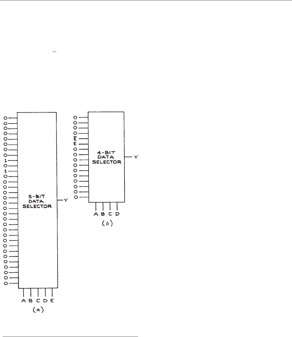
selector [see Figure 6.99(b)] can also be used by employing
a foldback arrangement. Looking at the A, B, C, and D bits,
one sees that there are 16 pairs of combinations of A, B, C,
and D that are independent of whether E is 1 or 0. For each
of the 16 pairs, the function Y is independent of the state of
E, equals E, or equals
E. The 16 input lines of the 4-bit data
selector will each have 0, 1, E,or
E attached to them.
Even more complexity can be built into the circuit by
having time delays on the functions so that one valve is not
opening while the other is closing. Extra functions, such as
turning on and off and venting the mechanical pump, can
also be added. This systematic method of analysis ensures
that nothing is overlooked. By noting when two functions
change state upon the change of state of a variable, deci-
sions about sequencing can also be made.
6.6.10 Implementing Logic Functions
Implementing functions with transistor gates requires that
the 0 and 1 states be associated with voltage or current
levels. There are a large number of logic families, all of
which have internally consistent 0 and 1 levels, but which
are not necessarily compatible. The choice of a logic fam-
ily for the implementation of a given function depends on a
number of factors – among them are speed, power dissi-
pation, immunity to noise, number of available functions,
cost, and compatibility with external circuits and other
logic families. A summary of the properties of the most
common logic families is given in Table 6.35. As can be
seen
from the table, there is a tradeoff between speed and
power dissipation – the fastest logic dissipates the most
power per gate and the slowest dissipates the least. In an
effort to reduce power dissipation while maintaining
speed, nominal voltage levels have been reduced to 3.5
and as low as 2.5 V for some logic families from the nom-
inal TTL 5 V. Noise immunity is measured by noise mar-
gin, the meaning of which is illustrated in Figure 6.100.In
general,
logic families are not directly compatible – trans-
lator chips exist for interfamily conversion, and some sim-
ple conversion circuits are given in Figure 6.101. The
abbre
viations SSI, MSI, LSI, and VLSI stand for small-
scale integration, medium-scale integration, large-scale
integration, and very large-scale integration, and are used
to specify the number of gates on a chip. SSI is less than 12
gates per chip, MSI is between 12 and 100, LSI is more
than 100, and VLSI is more than 1000. Simple logic func-
tions employ SSI and MSI.
The most common logic family has been TTL (transistor-
transistor logic) and its variations, but CMOS logic (com-
plementary symmetry, metal-oxide semiconductor) has now
largely displaced TTL because of its low power consump-
tion and wide range of usable power-supply voltages.
Emitter-coupled logic (ECL) is only used when the highest
speeds are required. The ECL 10 000 series is a slower
version of the ECL II series and is not so sensitive to the
quality of the interconnections. With the II series, a circuit
Figure 6.99 Implementation of the Y-function of the truth
table of Table 6.34 with (a) a 5-bit data selector and (b) a 4-
bit
data selector using a fold back arrangement.
464 ELECTRONICS
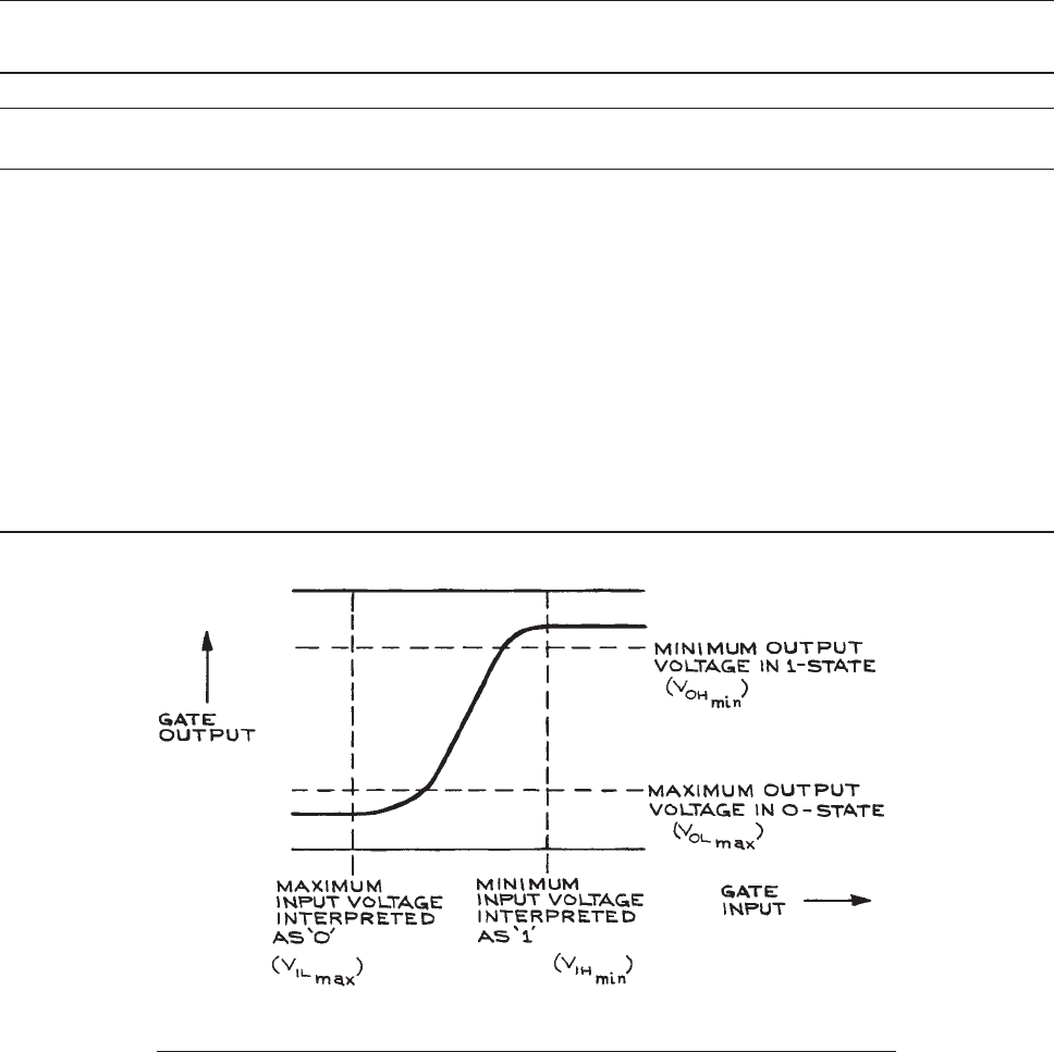
board with a ground plane must be used and the intercon-
nections carefully laid out to minimize cross-coupling.
Important changes in the semiconductor electronics
industry in the last few years reflect new technologies as
well as new philosophies in electronics. Whole new fam-
ilies of logic have been born – based on CMOS, Schottky,
and gallium arsenide (GaAs) technologies. Portable elec-
tronic devices from laptop computers to cell phones and
personal digital assistants require high-speed and low-po wer
electronics. The inherently lo west-po wer technology is
Table 6.35 Logic families
Logic
Family
Propagation
Delay (ns)
Power Dissipation
(mW/gate)
0-Level (V) 1-Level (V) Noise Margin,
Low/High (V)
Fanout Power
Supply (V)
TTL:
54/74 10 10 0.2 3.9 0.3/0.7 10 +5
54/74LS 10 2 0.2 3.9 0.3/0.7 20 +5
54/74F 4 4 0.2 3.9 0.3/0.7 33 (50LS) +5
CMOS:
54/74C 30 0 0.2 4.8 0/7/0.6 >50 (10LS) +5
54/74HC 10 0 0.2 4.8 0.7/0.6 >50 (10LS) +5
54/74HCT 8 0.010 0.2 4.8 0.7/0.6 >50 (10LS) +5
4000 CD
V
DD
= 5V 115 0.005 0.05 4.95 1.0 50 +5
V
DD
= 15V 40 0.060 0.05 14.95 2.5 50 +15
ECL:
10,000 3 24 1.75 0.90 0.3/0.3 10 5.2
100,000 0.8 40 1.75 0.90 0.3/0.3 10 4.5
Figure 6.100 Illustration of ‘‘noise margin.’’ Noise margin for
1-state ¼ V
OHmin
-V
IHmin
, noise margin for 0-state ¼ V
ILmax
–V
OLmax
.
DIGITAL ELECTRONICS 465
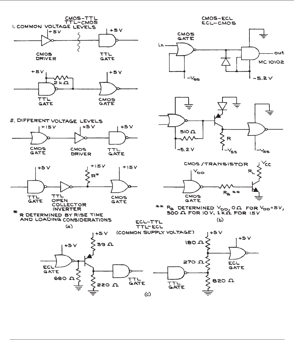
Figure 6.101 TTL, CMOS, ECL, and discrete transistor interface circuits. (a) CMOS-TTL and TTL-CMOS (the value of R is
determined by rise time and loading considerations). From McMOS Integrated Circuits Data Book, Motor ola, Inc, 1973.
Copyright of Motorola, Inc. Used with permission. (b) CMOS-ECL and ECL-CMOS (R
B
is determined by V
DD
:0X for V
DD
¼5V,
500 X for V
DD
¼ 10 V, 1 k X for V
DD
¼ 15 V); (c) ECL-TTL and TTL-ECL (from MECL System Design Handbook, 2nd edition, W.
R. Blood, Jr., and E. C. Tynan, Eds., Motorola Semiconductor Products, 1972. Copyright of Motorola, Inc. Use d with
permission.)
466 ELECTRONICS

CMOS, but it has suffered in the past from low speed. This
has largely been overcome with the HC and HCT logic
lines. Both are directly compatible with the older TTL
LS families, but offer greatly improved speed-to-power
ratios. Because TTL high levels can be as low as 2.2 V,
there can be difficulties driving HC devices from TTL out-
puts. This is overcome with the HCT family, which is
completely compatible with TTL over the full range of
TTL operating parameters. The HC logic has now replaced
the TTL LS family. The 4000 D series of CMOS can
operate with supply voltages from +5 to +15 V and is used
in conjunction with higher-voltage analog circuits.
FAST
[TM]
logic is based on Schottky technology and
approaches ECL 10 000 logic in speed, but with much
lower power consumption. FAST devices bear the desig-
nation 54/74F and have the advantage of TTL logic levels
while avoiding the smaller voltage swings and lower noise
margins of ECL.
7
FAST is a trademark of Fairchild Cam-
era and Instruments Corporation and is an acronym for
Fairchild Advanced Schottky TTL.
Because TTL is still used in some applications, a few
simple TTL circuits are given in Figure 6.102. The mechan-
ic
al contact conditioner [Figure 6.102(a)] ensures that the
ou
tput from a mechanical switch will be a single transition
rather than the series of voltage spikes normally resulting
from the mechanical bouncing of the contacts. Transistor-
transistor logic gates are either edge or level triggered. Edge
triggering refers to the transition between the 0 and 1 levels
(positive edge) or 1 and 0 levels (negative edge). Level
triggering occurs when the 0 or 1 is attained. Data sheets
specify the type of triggering each logic unit requires.
With most logic families, there is the tendency to gen-
erate current spikes during switching; this creates power-
supply noise. To reduce this noise, the power supply must
be decoupled with capacitors from the logic circuits. A
0.01 lF ceramic capacitor for each gate and an additional
0.1 lF capacitor for each 20 gates are generally sufficient.
Counters and shift registers are especially sensitive to
power-supply noise and should be decoupled with a 0.1 lF
capacitor for every two devices. For optimum perform-
ance, unused inputs should be set to logic level 0 by direct
connection to ground or logic level 1 by connection to the
power-supply voltage through a 1 to 10 kX resistor.
Some additional features of TTL are three-state outputs
and open-collector outputs. A three-state output has the
standard 0 and 1 levels and also a high-impedance, inac-
tive state . In this state, the output assu mes the level of any
active output connected to it. The three-state outputs are
designed to be connected together in a common line or
bus structure so that when any single output is active, a ll
the others assume its level. The open-c oll ec tor output
requires a collector resistor to the power supply for oper-
ation. When connected together, open-collector outputs
allow one to implement an output AND function (often
incorrectly termed wired-OR) that is, when any output is
0, all become 0. Open-collector outputs have the disad-
vantageofreducedtransitionspeedandhighoutput
impedanc e in the 1 sta te. They are usuall y used as line
drivers.
6.7 DATA ACQUISITION
6.7.1 Data Rates
When designing an experiment, one important considera-
tion is the rate at which data are collected. It is usually
useful to think of an experiment in terms of sampling rate,
sampling time, and measurement precision. Consider a
spectroscopy experiment where the output of a monochro-
mator is incident on a photomultiplier tube – the output of
which are pulses of electrons that are recorded with a coun-
ter. The monochromator is stepped at a regular rate and
predetermined step size over the wavelength interval of
interest. The time spent at each step combined with the
number of steps determines the total number of counts
recorded. If the total number of signal counts in any interval
is C
S
and the number of noise counts is C
N
, the total number
of counts, C
T
,isC
S
þC
N
. The statistical uncertainty in C
T
is
ffiffiffiffiffiffi
C
T
p
, and that in C
N
is
ffiffiffiffiffiffiffi
C
N
p
. The uncertainty in determin-
ing C
S
is therefore
ffiffiffiffiffiffiffiffiffiffiffiffiffiffiffiffiffiffi
C
T
þ C
N
p
, so the relative uncertainty is
ffiffiffiffiffiffiffiffiffiffiffiffiffiffiffiffiffiffi
C
T
þ C
N
p
=ðC
T
C
N
Þ. The counts increase linearly with
the time of measurement, but the relative uncertainty only
decreases as the inverse square root of the time of the meas-
urement. The data rate is the number of counts in a meas-
urement interval divided by the interval time.
Bits, bytes, wor ds, and characters are all used to specify
the amount of information. The number of bits necessary
to specify a given integer decimal D is given by N ¼
3.32 log
10
D. If N is a noninteger, it is rounded to the next
higher integer. If the decimal number is signed (that is, plus
DATA ACQUISITION 467
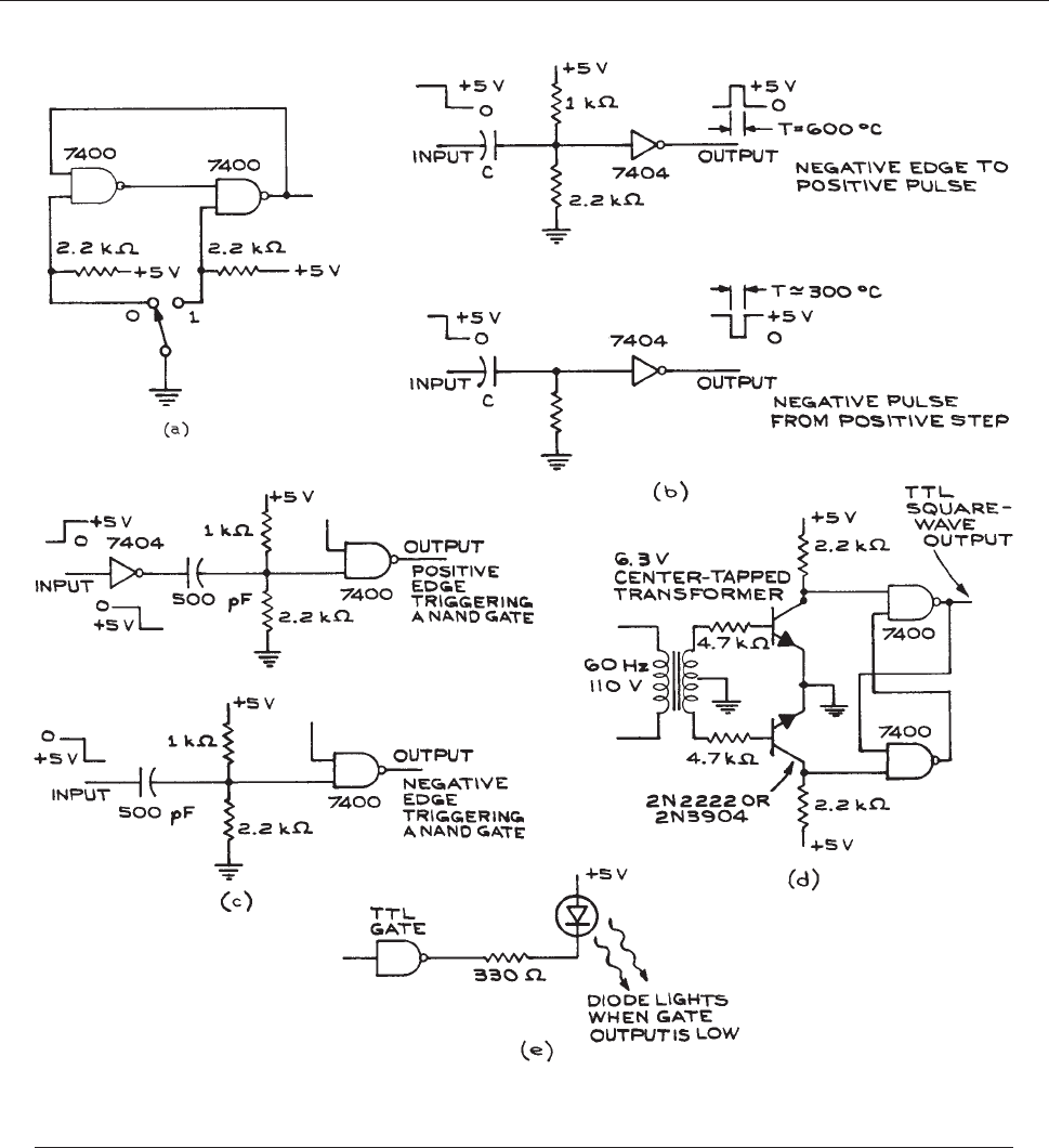
Figure 6.102 TTL signal-conditioning circuits: (a) mechanical-contact conditioner; (b) pulses from step inputs
(step duration must exceed output-pulse width); (c) edge triggering; (d) 60-Hz TTL square wave from the power line;
(e) TTL to LED.
468 ELECTRONICS

or minus), another bit is added. Eight bits make a byte, and
two bytes (16 bits) commonly, but not always, make a word.
A character is the equivalent of one word. If data are to
be transferred from the counter to a printer or other display
or storage device, the data acceptance rate of the device
must match the data output rate of the counter. Data rates
are often specified as a baud rate, which is the number of
times per second there is a transition on the signal line
from 0 to 1 or from 1 to 0.
For two devices to be compatible, a number of param-
eters must match. These include frequency response, volt-
age levels, timing, format, code, hand-shaking protocols,
and housekeeping procedures.
6.7.2 Voltage Levels and Timing
The most positive and most negative voltages correspond-
ing to the two logic states must match. For example, TTL 0
and 1 logic levels are þ3.2 and þ0.2 V, while ECL 0 and 1
levels are 0.75 and 1.55 V. Furthermore, the sign of the
logic must be identical – that is, positive or negative. Pos-
itive logic means that the more positive voltage level is
taken as a logical 1, and the more negative as logical 0.
The reverse is true for negative logic. If the signs do not
match and everything else is satisfactory, only inversion of
the input signal will be required.
Often a digital input or output circuit is compatible with
a logic family of which it is not a member. The 54/74C,
HC, and HCT families are TTL-compatible, for example,
which means that the voltage levels are compatible. The
sinking and sourcing capabilities may be very different,
however, for so-called compatible logic families. Sinking
has to do with the number of gates that can be attached to
the output of a single gate and still maintain reliable oper-
ation. With TTL logic, when an output is at logical 0 it
must be able to hold all inputs connected to it at logical 0.
Since this condition is a consequence of the input transis-
tors being in saturation, the output must be able to sink all
the saturation currents and still keep the inputs at their
required levels. A TTL output at logic level 1 attached to
a TTL input will turn off the input transistor, and very little
current will flow in the input circuit. This is the sourcing
specification. Fan-in and fan-out are directly related to the
sinking and sourcing capabilities of a gate. Fan-in is the
maximum number of logic inputs to a gate for reliable
operation, while fan-out is the number of logic outputs it
can drive reliably. These specifications should be carefully
considered when connecting two different logic families.
Timing is also important – the required rise and fall times,
as well as pulse widths, must be compatible. Timing dia-
grams show the relationship between signals and should be
consulted. Converter chips that change the signals from
one logic family directly to another are available.
6.7.3 Format
A serial format has all data on a single line in a sequential
pattern. This is economical as far as wiring is concerned,
but slower than a parallel format where there can be as
many data lines as bits, and all of the bits in a word are
transferred at the same time. This is the fastest way to
transmit data, but the least economical.
There are also parallel-serial formats where the data are
transmitted in sequential parallel codes. An eight-bit byte,
for example, could be transmitted with four lines as two
four-bit words. A synchronization code is necessary with
such an arrangement to be able to distinguish between the
beginning and end of a single byte string. It is possible
to convert from a serial code to a parallel code and vice
versa with converters that use shift registers. For serial-to-
parallel conversion, data are sent to the registers from
one end and then read from the outputs of each stage. For
parallel-to-serial conversion, data are put into each register
simultaneously and then extracted from the last register
sequentially, a bit at a time. Data transmission in one direc-
tion over a single line is called simplex, in two directions
over a single line is called half duplex, and in two directions
simultaneously, with a single line and two coding frequen-
cies or two separate lines, is full duplex. Data conversion
ICs called universal asynchronous receiver-transmitters
(UARTs) take a wide variety of data formats and convert
them to standard codes, one of which is ASCII (American
Standard Computer Information Interchange). The ASCII
computer code is given in Table 6.36.
A
major difficulty in setting up data-handling equipment is
the interface. The RS232C serial interface can handle data
rates to 20 kbps – it has a high input impedance (3 to 5 kX),
uses relatively high voltage (þ25 V), and is unbalanced and
therefore noise-susceptible. The pin assignments for the
DATA ACQUISITION 469

standard 25-pin connector used with this interface are giv en in
Figure 6.103. More adv anced interfaces such as the RS485
us
e balanced circuitry and can handle data rates well in excess
of 10 Mbps (megabits per second). There are computer inter-
faces designed to handle data rates to hundreds of Mbps.
Modems (modulator-demodulators) are devices for
converting a binary code to audio frequencies (300 to
3300 Hz) for transmission over telephone lines, and recon-
verting the audio frequencies to binary. They are separate
units to which both a telephone receiver and a data termi-
nal can be attached.
6.7.4 System Overhead
In all data-transmission schemes there are additional sig-
nals that are nec essary to assure that the data transfer
occurs correctly. These are sometimes called housekeep-
ing signals. In the c ase where such information is
exchanged back and forth between the sending unit and
the receiving uni t, they are called hand-shaking.These
additional signals contribute to what is called the system
overhead – that is, additional data c apacity which must
exist independent of the useful information transmitted.
When data are transferred at a regular rate between two
units, they must be kept in step. A sync bit is often used to
assure synchronization between the two units. When
data are transferred at a variable rate that depends on
other independent parameters of the system, they are
said to be asynchronous. In this case, the sending unit
must ale rt the receiving unit of t he c oming of data, and
the receiving unit then should give a ready to receive
signal, after which the data are transferred. When
data transfer is complete, an end of data signal is also
usually sent. Without these signals, there can be no reli-
able data transfer.
To ensure the reliability of data transfer and detect errors
in the transmission, an extra parity bit can be sent. One
scheme requires the parity bit to be 1 when the sum of the
data bits is even and 0 when the sum is odd (see Table
6.29). At the receiving unit, data bits are summed and
compared with the parity bit – if there is consistency, the
data are accepted; if not, they are rejected. A more
Table 6.36 ASCII computer code
00001111)b
7
b
4
b
3
b
2
b
1
00110011)b
6
YYYY01010101)b
5
0000NULDLESP0@P\ p
0001SOHDC1! 1AQaq
0010STXDC2$ 2BRbr
0011ETXDC3# 3CScs
0100EOTDC4$ 4DTdt
0101ENQNAK%5EUeu
0110ACKSYN&6FVfv
0111BELETB# 7GWgw
1000BS CAN( 8HXhx
1001HT EM ) 9I Yiy
1010LF SUB
*
:JZjz
1011VT ESC+ ; K[ k{
1100FF FS , <L\ l |
1101CR GS ¼M] m}
1110SO RS . >N^n~
1111SI US / ?O_oDEL
7-bit code gives 2
7
¼128 different words Columns 1 and 2 are machine commands such as carriage return (CR), line feed (LF), escape
(ESC), etc.
470 ELECTRONICS
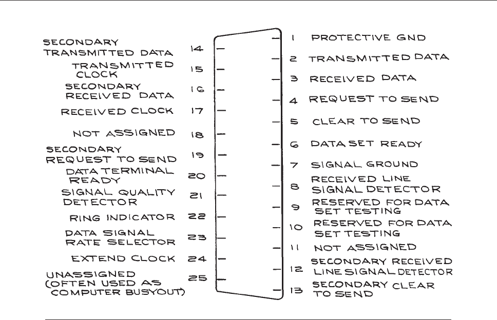
elaborate way of ensuring integrity is to have the receiving
unit echo the received data back to the sender, where they
are compared with the original data. Any differences cause
the data to be rejected. This system minimizes transmis-
sion errors at the cost of additional complexity and lower
speed.
Returning to the example of the spectroscopy experi-
ment in Section 6.7.1, if the expected signal produces
10
4
counts per second and the background is 10 counts
per second, the statistical error after one second is
ffiffiffiffiffiffiffiffiffiffiffiffiffiffiffiffiffiffi
10
4
þ 10
p
=10
4
ffi 1%. If the counting interval is one sec-
ond, at least 13 bits are needed for the data alone. To be
safe, 16 bits should be used, with the extra bits reserved for
housekeeping functions. This data transfer rate of 2 bytes
per second is very modest. It is necessary, however, to
consider the true rate of data transfer. If the data are held
on the output lines of the counter for only 10 ms, the
effective rate is 200 bytes per second.
In order to reduce the timing requirements of the counter, a
latch can be used on the output lines to hold the data for a
predetermined amount of time regardless of the subsequent
status of the lines. The operation of a 4-bit latch based on four
D flip-flops (Table 6.31) is illustrated in Figure 6.104.Dataat
the
input lines to the latch (A
0
,A
1
,A
2
,andA
3
) are transferred
to the output lines (B
0
,B
1
,B
2
,andB
3
) when the control line
is activ ated. In the absence of a start signal on the control line,
the output levels cannot change even though the input levels
do. In this way, data can be held on the output lines for a time
suffi cient for them to be processed by the subsequent data-
receiving unit. The timing relations among the various signals
are important for proper operation of the latch. The control
signal must arriv e when there are valid data on the input lines.
A data buffer serves a purpose similar to a latch. It holds
receiv ed data for processing by subsequent units or circuits.
Printers, which are inherently slow because they are mechan-
ical devices, often have data b uf fers that hold the input data
Figure 6.103 RS232C serial interface: 25-contact connector pin assignment.
DATA ACQUISITION 471
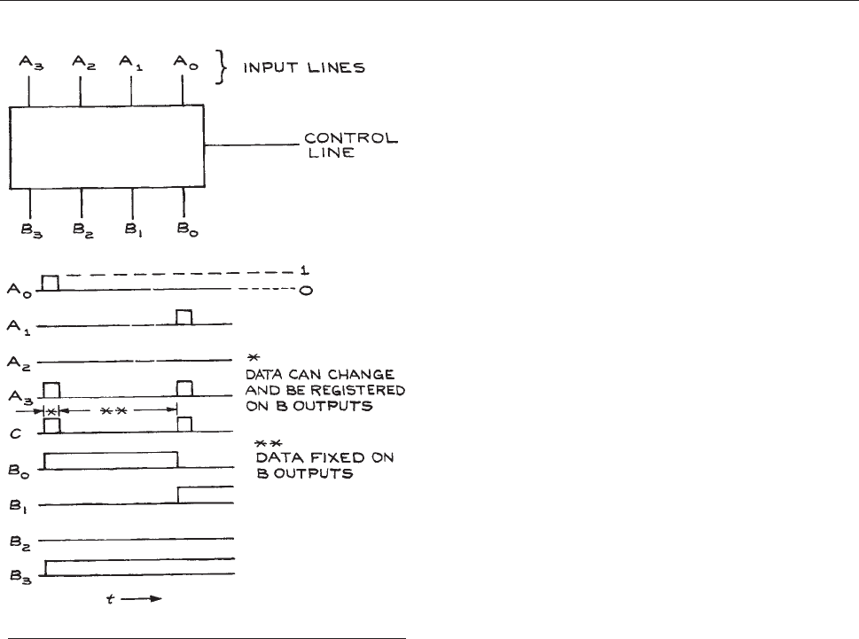
until the printing mechanisms can transfer them to paper.
The buf fer is then ready to accept another batch of data.
6.7.5 Analog Input Signals
The spectroscopy experiment discussed above could be
modified by using a detector with an output current propor-
tional to the incident light intensity, as in Figure 6.105.To
con
vert the current to a digital signal requires an ADC. The
resolution of the ADC is determined by the number of
output bits, and the analog signal must be compatible, both
in magnitude and in sign, with the input requirements of
the ADC. If the ADC accepts only a voltage with a max-
imum full-scale value of 1.0 V and the analog signal has a
current maximum of 10
8
A, conversion from current to
voltage can be made using an operational amplifier with a
variable-gain element. Response and sampling times must
be considered. The analog input to the ADC must remain
constant long enough for the ADC to respond. This is
called the settling time. For times less than the settling
time, the ADC output will not be a valid representation
of the analog input.
Voltage-to-frequency converters provide an easy way to
convert analog signals into digital form. Consider the
AD537 converter manufactured by Analog Devices as an
example. Through the selection of two external resistors
and a capacitor, frequencies up to 100 kHz can be generated
with a maximum input current of 1.00 mA. The circuit for a
full-scale input of 1 V and a 10 kHz frequency maximum is
given in Figure 6.106. The combination of the 8.2 kX re
sis-
tor and 5 kX potentiometer sets the gain of the circuit. The
potentiometer is adjusted so that the output frequency is
10 kHz for a 1 V input. The 20 kX potentiometer nulls the
offset voltage of the input amplifier. The linearity is
0.05 % of full scale at 25 °C, with a temperature coefficient
of þ30 ppm of full scale per °C. To minimize noise, a
simple low-pass filter is used at the input. The 5 kX load
resistor, R
out
, allows the circuit to be reliably connected to
TTL logic. The circuit can be used to convert an analog
voltage to a digital word by connecting the output to a gated
counter. A four-digit decade counter gated for 1s will regis-
ter the input voltage to four significant figures. A similar
circuit can be used to convert the output of an analog elec-
trometer to a digital format.
The circuit can also be used to integrate a varying analog
signal, as long as the signal variation occurs in a time that
is much longer than the reciprocal of the maximum fre-
quency. The area under the peaks in a gas chromatogram,
for example, can be recorded by connecting the output
from the chromatograph to a voltage-to-frequency con-
verter and using a counter to total the number of output
pulses. The scale factor depends on the maximum fre-
quency and full-scale input voltage.
Voltage-to-frequency converters can also be used for
frequency-to-voltage conversion. In this configuration, the
input can be a TTL pulse train and the output is a voltage.
The circuit can be used as an FM demodulator, frequency
monitor, or motor speed controller. The AD537 voltage-to-
frequency converter, made by Analog Devices,
Figure 6.104 A 4-bit latch.
472 ELECTRONICS
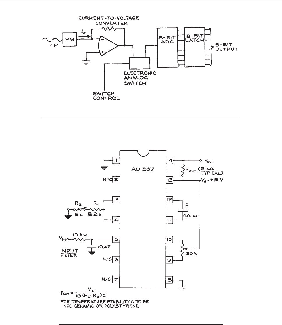
Figure 6.105 Example of a light-measuring system using an ADC with a
sample-and-hold circuit at the input.
Figure 6.106 Voltage-to-frequency conversion circuit. A 1.00 V input gives
a 10 kHz output frequency.
DATA ACQUISITION 473
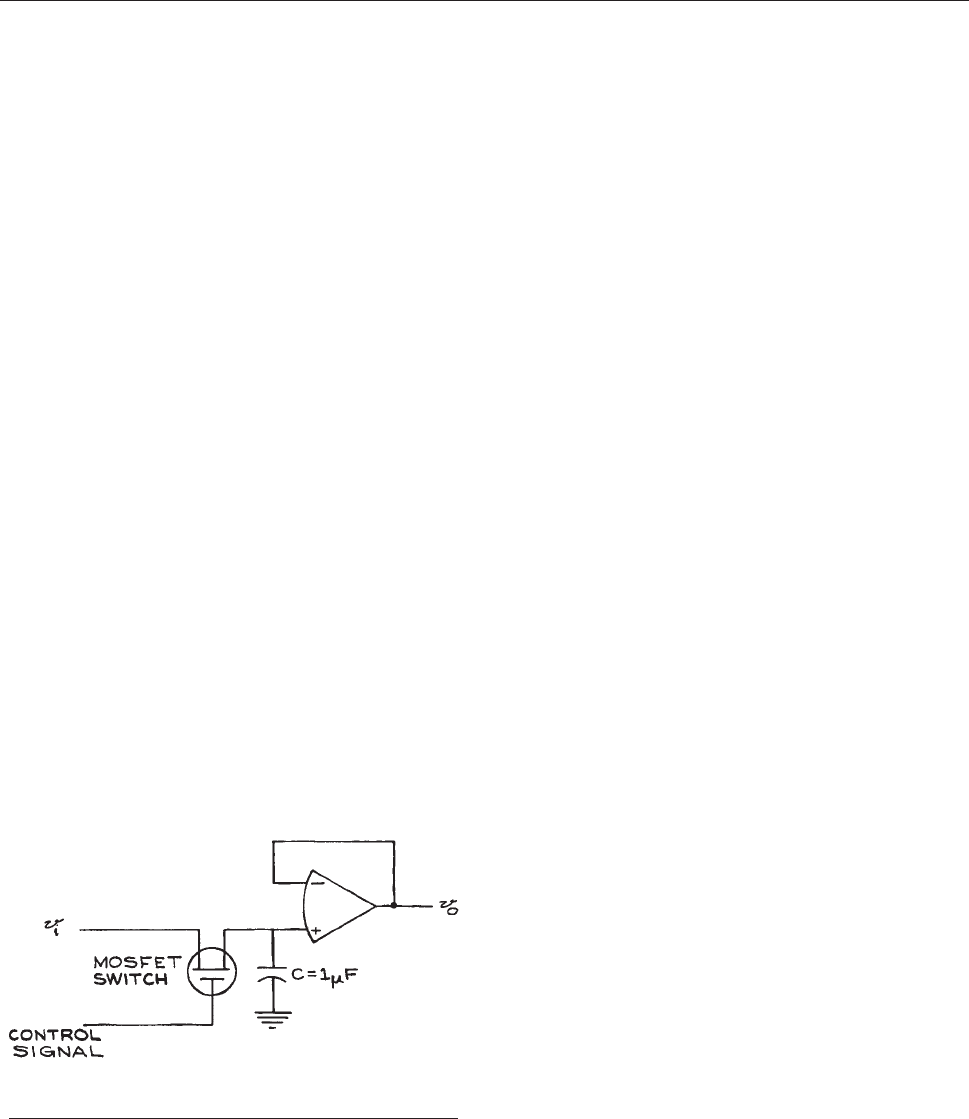
accommodates positive or negative input voltages and
negative currents. It operates from a single 5 to 36 V supply
and has a maximum full-scale frequency output of
100 kHz.
For the systems under consideration, the output current
must not be changing faster than the ADC can respond.
When the analog signal is changing too rapidly, a sample-
and-hold, S/H, circuit can be used ahead of the ADC.
Important parameters of a S/H circuit are the sampling
time and the output decay time. S/H circuits use a capacitor
as a memory element, with the sampling time proportional
to the capacitance. Because of leakage, capacitors cannot
permanently maintain their voltage – fast sampling circuits
with small capacitors maintain their output voltages for
much less time than slower circuits. The decay time is
the time for the output to fall to a fixed fraction of the
original value. A figure of merit for S/H circuits is the ratio
of sampling time to decay time. For the simple S/H circuit
shown in Figure 6.107, a control signal closes the MOS-
FET
switch, and the 1 lF capacitor is charged with a time
constant R
on
C, where R
on
is the on resistance of the switch.
Typical values of R
on
are 10
2
to 10
4
X, giving a time con-
stant of 10
4
to 10
2
s for the sampling time. The decay
time depends on capacitor leakage, the off resistance of the
MOSFET, and the bias currents of the operational ampli-
fier. When high-quality capacitors with polyethylene, pol-
ystyrene, polycarbonate, or Teflon dielectrics are used,
most of the decay will be due to current through the switch
(~10
9
A) and bias currents (10
9
to 10
8
A for an average,
low bias-current operational amplifier). In this example,
the decay will be of the order of 2 to 20 mV/s. Special
MOSFET switches and operational amplifiers with
picoampere bias currents can reduce these decay times
even further.
6.7.6 Multiple Signal Sources: Data Loggers
A multiple-transducer, data-acquisition system is a
straightforward extension of the s ingle-transducer sys-
tem already described. Figure 6.108 shows one po ssible
a
rrangement. Such systems are useful when it is neces-
sary to monitor and recor d several d ifferent signa ls at
virtually the same time. If the transducers all have analog
outputs, the most convenient arrangement is an analog
multiplexer. The function of the multiplexer is to alter-
nately connect each of the analog signal lines to an ADC
circuit a nd the recordin g instrument. The switching
between the various signal lines is accomplished by sep-
arate control li nes. Multiplexing reduces the number of
circuit components at the expense of more complex con-
trol and synchronization circuits. With the system in
Figure 6.108, the data rate can be as much as four times
that
of a simple system.
6.7.7 Standardized Data-Acquisition
Systems
A number of companies manufacture complete data-
acquisition units specifically designed for the laboratory.
As long as the input signals are compatible and the data
rates are within the limits of the unit, they provide a fast
and efficient means of constructing a data-acquisition
system. Data acquisition from multiple sensors is a com-
mon industrial situation and there are several kinds of
industrial data loggers. These, however, are designed for
reliability rather than flexibility and are generally not
suited to laboratory data acquisition, where many different
kinds of transducers are used. There are two standardized
laboratory data-acquisition systems, nuclear instrumenta-
tion module NIM and CAMAC.
The NIM system consists of individual electronic units
that fit into a mounting frame or bin, which has a central
power supply. The NIM bin is capable of powering several
individual units, depending on their size. The bin power
supply provides 624 V, 612 V, and usually 66V. Each
full-size bin has 12 slots in which instrument module units
Figure 6.107 A sample-and-hold circuit using a capacitor
as a memory element.
474 ELECTRONICS
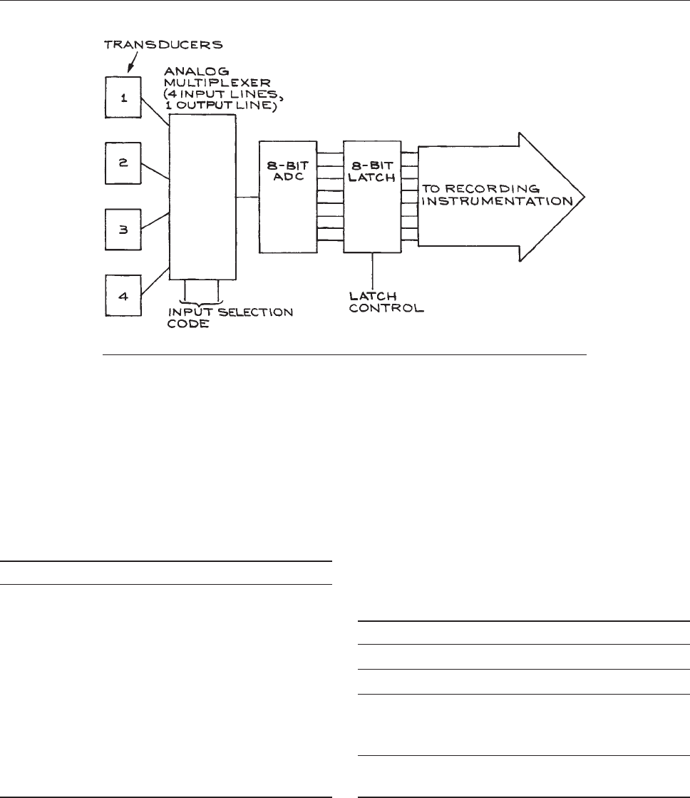
can be placed. Units can occupy anywhere from one to six
slots. The bin power supplies and individual units have
been designed so that a bin can accept the full comple-
ment of modules without becoming overloaded. A short
list of standard NIM modules is given in Table 6.37. Inter-
conne
ctions between modules are made with coaxial
cable. In older units, B NC connections are common;
newer units use higher-density, LEM O- typ e connectors.
Input and output specifications are standardi ze d so th at
NIM modules can be connected together without compat-
ibility concerns. The NIM logic level specifications are
given in Table 6.38.
Originally
the NIM standard voltages were 612 V and
624 V. As the use of integrated circuits increased, a 66V
voltage was included in the standard. Modules operating from
612 V and 624 V supplies, howe v er , are still the most flex-
ible, because all bins have these voltages. Where 66V is
required for a module in a 612/624 V bin, it is best to derive
it from within the module using the av ailable 612 V. Use of
Figure 6.108 A multiple-transducer data-acquisition system using a multiplexer.
Table 6.37 Modules available in NIM
Power supplies
Preamplifiers, amplifiers
Discriminators
Coincidence units
Delays
Signal generators, pulse generators
Counters/timers
Gates
DACs and ADCs
Analog adders, subtractors, dividers, multipliers
Time to amplitude converters (TACs)
Signal averagers
Multichannel analyzers
Table 6.38 NIM Logic Levels
Output (must deliver) Input (must accept)
Digital Data
Logic 1 þ 4toþ 12 V þ 3toþ 12 V
Logic 0 þ 1to2V þ 1.5 to 2V
Fast Logic (50 X impedance)
Logic 1 14 to –18 mA 12 to 36 mA
Logic 0 1toþ 1mA 4toþ 20 mA
DATA ACQUISITION 475

high-current, 6 V modules in a 612/624 V bin should be
av oided because the regulation of the 612 V and 624 V sup-
plies will be degraded by the high current in the common
return line. Precise reference voltages should be produced in
the modules themselves, since the bin voltages hav e relatively
wide tolerances, 624.0 (þ0.7%), 612.0 (þ1.0%), and 66.0
(þ3.0%). The NIM po wer-connector pin assignments and
other details are given in Figure 6.109. The NIM standard
lo
gic levels are not compatible directly with common logic
families such as TTL or ECL. The po wer-suppl y voltages are
also different from common logic supplies (þ5V) and opera-
tional-amplifier supplies (þ15V). Some con version circuits
between NIM, ECL, and TTL le vels are gi ven in Figure 6.110.
N
uclear instrumentation module systems are limited
in complexity to hard-wired interconnections between mod-
ules. This becomes cumbersome when there are several
modules that must be linked together. To circumvent the
limitations of NIM systems, the CAMAC system was devel-
oped. This system retains the use of individual modules that
can be plugged into a central power supply unit – in this
Figure 6.109 NIM connector pin assignment (GP ¼ guide pin, GGP ¼ ground guide pin, GS-1 ¼ guide socket, GGS ¼
ground guide socket).
476 ELECTRONICS
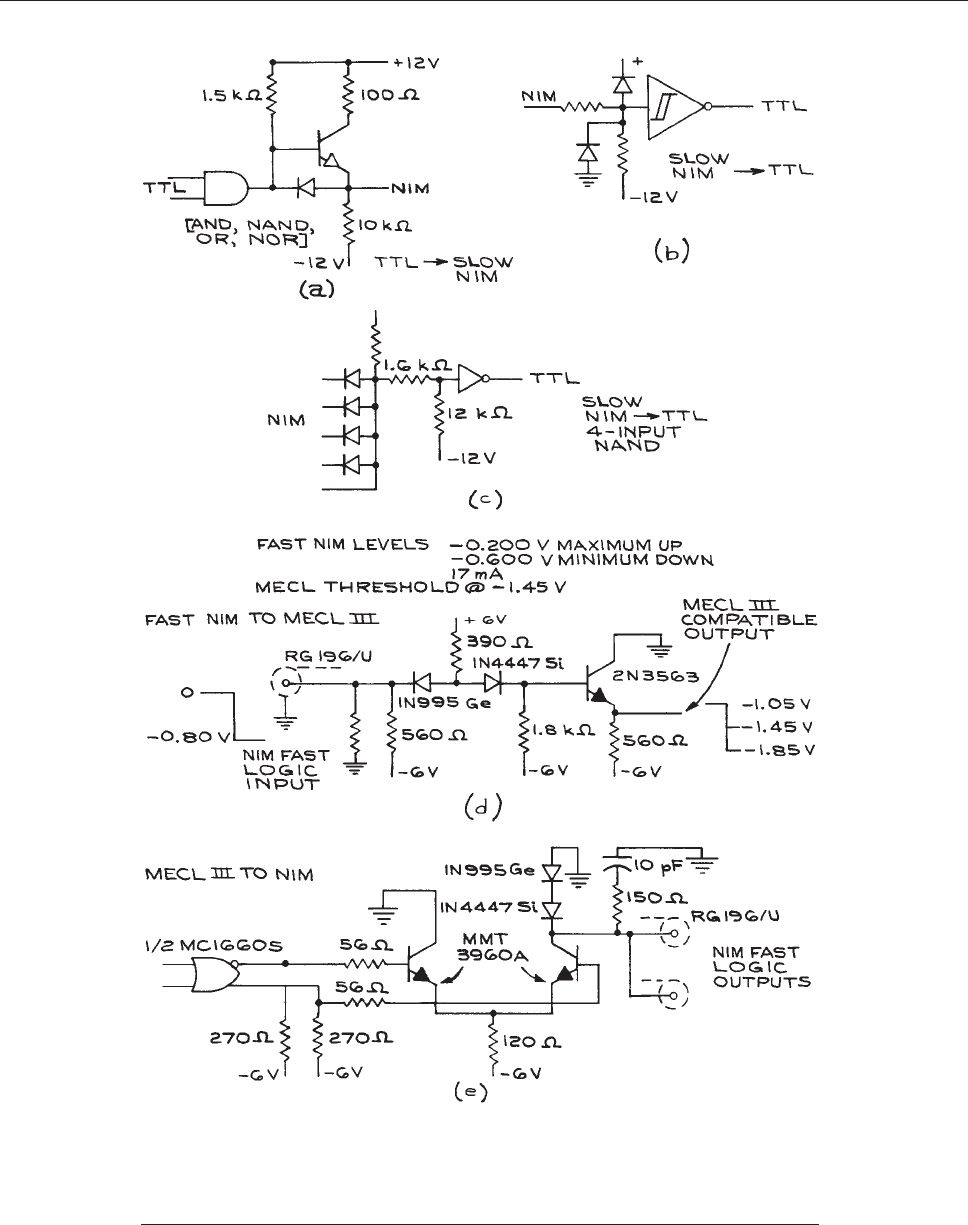
Figure 6.110 (a) TTL-NIM conversion circuit, (b) Slow NIM-TTL conversion circuit, (c) Slow
NIM-TTL with a 4-input NAND gate, (d) Fast NIM to MECL III, (e) MECL III to fast NIM. (fast
NIM levels 17 mA, 0.200 V maximum high, 0.600 V minimum low; MECL threshold
–1.45 V. (From R. F. Nagel, NIM Fast Logic Modules Utilizing MECL III Integrated Circuits,
IEEE Trans. Nucl. Sci., NS-19, 520, 1972. Copyright 1972 IEEE.)
DATA ACQUISITION 477
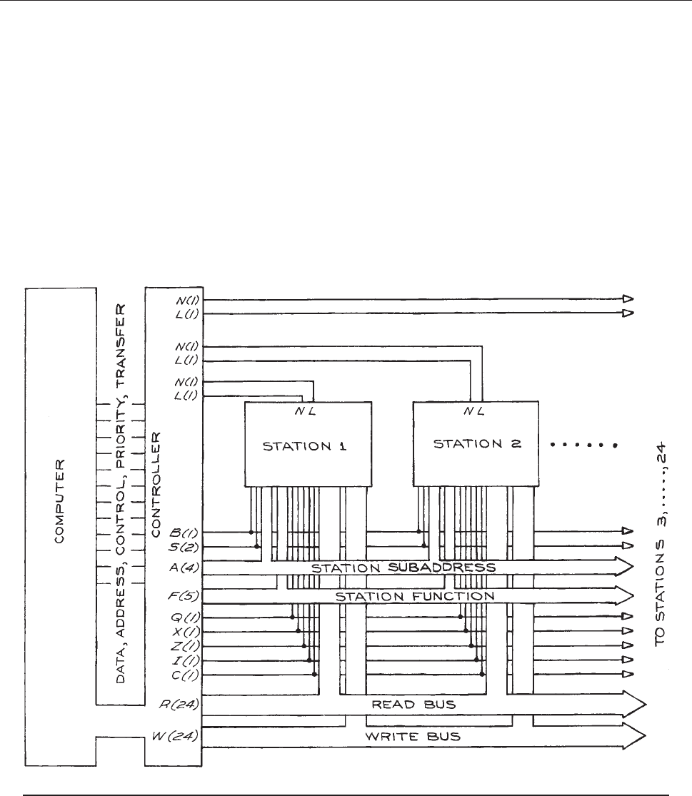
case, a crate. The CAMAC crate, however, has a large
number of additional lines besides those for the power.
The additional lines form the data bus. The bus has 24
read and 24 write lines, 4 station sub-address lines, and 5
station function lines – each station has its own identifica-
tion line and look-at-me (LAM) line. Common to all sta-
tions are two timing lines, three status lines, and three
control lines. These lines are connected to the control unit
(crate controller). Also connected to the controller are the
lines from the computer, generally divided into a set of
data bits and address bits. The controller interprets the
signals from the computer and sends appropriate signals
to the individual CAMAC units or stations. This is shown
schematically in Figure 6.111, with the line designations
gi
ven in Table 6.39. With each of the units under digital
control,
it is possible, through the use of a computer con-
nected to the crate controller, to have systems capable of
extremely complex logic and control functions. Data can
be collected by the computer and stored, displayed, and
manipulated with a degree of complexity limited only by
the programming language used by the computer.
The CAMAC system offers hardware and software
compatibility among individual units. P rogramming
can be a formidable task because the information trans-
ferred between the crate controller and the computer is
a binary machine-language code that has no relation to
Figure 6.111 The CAMAC bus.
478 ELECTRONICS
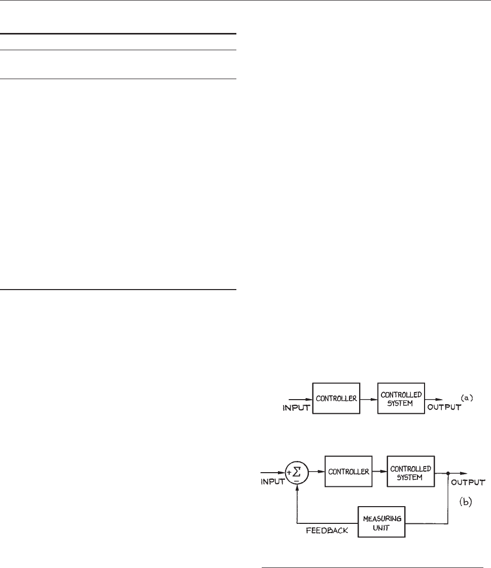
the high-level languages used for scientific calculations.
An alternative is to write the codes in a high-level lan-
guage, such as FORTRAN, and at appropriate points in
the program call a machine-language subroutine that con-
verts the FORTRAN variables to the bit code necessary for
control of the crate modules. When done in this way,
machine-language programming can be relatively simple.
A CAMAC system can represent a considerable invest-
ment in money and in the time necessary to learn the
required programming techniques. The need for a com-
puter to run the system properly – and the computer
peripherals such as terminals, printers, and mass storage
units – are additional expenses. The advantage of the
CAMAC system is the complete flexibility that it provides.
As in NIM systems, the individual modules are not costly
because there is no need for internal power supplies or
complex logic circuits. There are now several manufac-
turers offering lines of CAMAC crates, controllers, and
individual function modules. There are also NIM–
CAMAC adapters that permit one to run certain NIM mod-
ules under CAMAC control.
6.7.8 Control Systems
Control theory establishes a framework that enables one to
optimize an active system for accuracy, stability, transient
response, resistance to external perturbations, and internal
component changes. The method of analysis uses the Lap-
lace transform formalism in a way that is similar to that used
in circuit theory (see Section 6.1.5). Control theory is an
es
tablished engineering subject and there are many excel-
lent texts available. The purpose of this section is to give a
brief introduction to the subject and provide general infor-
mation on the analysis of systems and the proper configu-
rations for accomplishing given tasks.
All control systems, whether electrical, mechanical,
hydraulic, pneumatic, optical, thermal, acoustical, or elec-
tromechanical can be represented in terms of one of the
two block diagrams shown in Figure 6.112.
Th
e first system is open loop where the re is no signal
path from the output back to the input. An example is the
burner on the top of a stove. Once the position of the
burner switch or valve is set, there is no further control
over the burner output. The second system is closed loop,
in which a portion of the sampled output is sent back to
the input and compared with the input signal. An exam-
ple of a closed-loo p sys tem is the oven of a stove. The
temperature is s et by an external input and this input is
compared to a signal proportional to the temperature of
the oven. If the oven temperature exceeds the set
Table 6.39 CAMAC line designations
Line Code
(no. of lines used)
Command Function
N(1) Station number Selects station
A(4) Subaddress Selects section of station
F(5) Function Defines function
S(2) Strobe Controls phase of
operation
R(24) Read Parallel data to module
W(24) Write Parallel data from module
L(1) Look-at-me Request for service
B(1) Busy Operation in progress
X(1) Command
accepted
Module ready
Q(1) Response Status
Z(1) Initialize Sets module
I(1) Inhibit Disables module
C(1) Clear Clears registers
P(5) Extra lines
þ24V
þ6V
Power
Figure 6.112 Control system block diagram:
(a) open loop, (b) closed loop.
DATA ACQUISITION 479
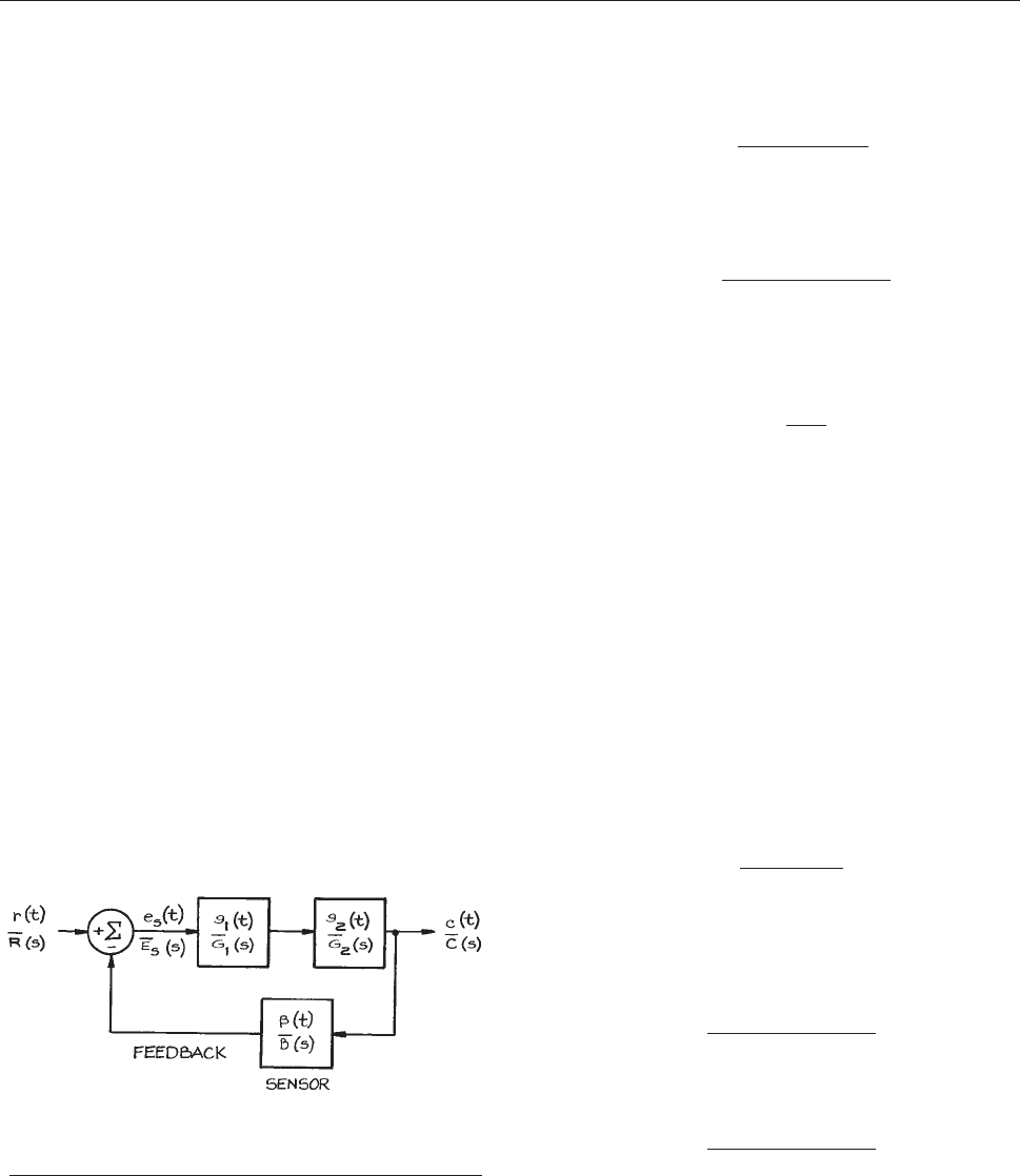
temperature, the oven heat source is turned off; if the
oven temperature is less than the set temperature, the
source is turned on.
The standard method for testing an open-loop system is
to apply s ignals at the inputs of each stage, starting with
the last and proceeding to the first – verifying the input
and output signals at each po int. This sequential testing
method cannot be used for a closed-loop system because
the input to each stage is related to the output of the
overa ll system.
All closed-loop systems have an input, an output, a sum-
ming or comparison unit, a controller, the working unit that
is controlled, a measuring or sampling unit, and a feedback
path. Once mathematical models for each of the units in the
system are developed and combined appropriately, the over-
all performance of the system can be evaluated and opti-
mized by varying the parameters of the model.
Each unit of a control system can be characterized by a
transfer or gain function. These functions describe how the
input to the unit is transformed by it and converted to the
output. The individual transfer functions themselves are,
in general, the solutions of ordinary, linear differential
equations that are most easily expressed in terms of Laplace
transforms (see Section 6.1.5). The full representation of
th
e system in terms of Laplace transforms is particularly
easy to assess with respect to stability, accuracy, and tran-
sient response.
Consider the general system shown in Figure 6.113 con-
sisting
of an input variable r(t), output variable c(t), and
transfer functions g
1
ðtÞ, g
2
ðtÞ and bðtÞ. The Laplace trans-
forms of these functions are
RðsÞ,
CðsÞ,
G
1
ðsÞ,
G
2
ðsÞ, and
BðsÞ respectively. The transfer function for the overall
system is:
gðtÞ¼
g
1
ðtÞg
2
ðtÞ
1 þ bg
1
ðtÞg
2
ðtÞ
ð6:52Þ
with the equivalent Laplace transform:
GðsÞ¼
G
1
ðsÞ
G
2
ðsÞ
1 þ
BðsÞ
G
1
ðsÞ
G
2
ðsÞ
ð6:53Þ
GðsÞ can be written as the ratio of two polynomials in s:
GðsÞ¼
PðsÞ
QðsÞ
ð6:54Þ
The roots of P(s) give the zeros of the transfer function,
and the roots of Q(s) give the poles of the transfer function.
The system is stable if the poles of the transfer function lie
in the left half of the complex s-plane.
System Response
(i) Sensitivity. Sensitivity S is a measure of the fractional
change in
GðsÞwith a fractional change in any part of the
system represented by the variable b. The smaller the S,
the less sensitive the system is to changes in any element of
the system:
S ¼
D
GðsÞ=
GðsÞ
Db=b
ð6:55Þ
As examples, S will be calculated for variations in the con-
troller transfer function
G
1
ðsÞand for the feedback,
BðsÞ:
Case 1: Relative change in
G
1
ðsÞ;
S ¼
1
1 þ
BðsÞ
G
1
ðsÞ
G
2
ðsÞ
ð6:56Þ
Case 2: Relative change in
BðsÞ;
S ¼
BðsÞ
G
1
ðsÞ
G
2
ðsÞ
1 þ
BðsÞ
G
1
ðsÞ
G
2
ðsÞ
ð6:57Þ
Figure 6.113 Block diagram of a generalized closed-loop
control system with schematic representations of the
transfer functions and their Laplace transforms.
480 ELECTRONICS
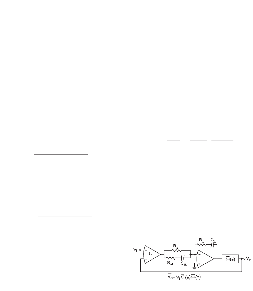
For Case 1, S is small when
BðsÞ,
G
1
ðsÞ, and
G
2
ðsÞ are
large. For Case 2, S is small only if
BðsÞ,
G
1
ðsÞ, and
G
2
ðsÞ
are small, so a system cannot simultaneously be made
insensitive to changes in the transfer function of the con-
trolled unit and transfer function of the feedback element.
The solution is to use a high-quality feedback element that
remains stable over a wide variety of conditions and to
increase the transfer functions of the other system elements
in order to stabilize the overall system with regard to their
changes.
(ii) Steady-state accuracy. The steady-state accuracy of a
system e
ss
ðtÞ is the difference between the input signal rðtÞ
and the closed-loop signal from the output bcðtÞ taken in
the limit as t ! ‘. In terms of Laplace transforms, the
difference between the input signal and the closed-loop
signal from the output is:
RðsÞ
BðsÞ½1 þ
BðsÞ
G
1
ðsÞ
G
2
ðsÞ
: ð6:58Þ
In s-space, the limit as t ! ‘ is obtained by multiplying:
RðsÞ
BðsÞ½1 þ
BðsÞ
G
1
ðsÞ
G
2
ðsÞ
ð6:59Þ
by s and taking the limit as s ! 0:
E
ss
¼ lim
s!0
RðsÞ
BðsÞ½1 þ
BðsÞ
G
1
ðsÞ
G
2
ðsÞ
: ð6: 60Þ
To evaluate
E
ss
, it is necessary to specify the signal
RðsÞ.
For a unit step input
RðsÞ¼1=s (see Table 6.2) so that
E
ss
¼ lim
s!0
RðsÞ
BðsÞ½1 þ
BðsÞ
G
1
ðsÞ
G
2
ðsÞ
: ð6: 61Þ
For simplification assume a unity feedback system so
that
BðsÞ¼1. If then
G
1
ðsÞ
G
2
ðsÞ is of the form
FðsÞ=s
N
QðsÞ, where FðsÞ and QðsÞ are polynomials in s
and N > 1,
E
ss
will approach zero and the output will
approach the input.
(iii) Proportional, Integral, and Differential (PID)
Control. The most general type of controller is one that
provides an output that is the sum of three terms – one
proportional to the difference between the reference sig-
nal and controlled signal, one proportional to the time
integral of the difference, and one proportional to the time
differen tial of the difference. These PID controllers use
operational amplifiers configured as direct gain elements,
integrators, and differentiators to attain these functions.
The Laplace transforms of the three functions give a
transfer function that has a form that depends on the
details of the operational-amplifier circuits. As an exam-
ple, consider the circuit in Figure 6.114.Ithasthetransfer
fu
nction:
GðsÞ¼
Kð1 þ sR
1
C
1
Þ
2
sR
1
C
1
ð1 þ sR
2
C
2
Þ
ð6:62Þ
for R
1
þ R
2
=R
1
¼ C
1
=C
2
,
GðsÞcan be rewritten as the sum
of three terms:
GðsÞ¼K 1 þ
1
sR
1
C
1
þ
R
1
R
1
þ R
2
1 þ sR
1
C
1
1 þ sR
2
C
2
ð6:63Þ
where the first term is the P, the second the I and the last the
D. The unit represented by the transfer function
HðsÞ has
been added to limit the frequency response and increase
the overall stability of the system. Commercial PID con-
trollers allow one to adjust the absolute as well as the
relative weights of each of the terms to attain the optimum
overall system response. This generally means a response
that has the maximum bandwidth consistent with a phase
margin of approximately 60°.
Figure 6.114 PID controller circuit.
DATA ACQUISITION 481

6.7.9 Personal Computer (PC)
Control of Experiments
Computer operation of experiments is best suited to rou-
tine measurements on systems with a high degree of
reliability – the latter condition is not always met for
ordinary laboratory experiments. It is not worthwhile
to add a computer to an experiment that is intended to
make a limited number of specialized measurements.
Though it may be tedious, it is often much more efficient
to take measurements by hand rather than purchase spe-
cialized measuring instruments, a computer or a com-
puter interface, and software, connect them together,
write the necessary software, and place the system i nto
operation. On the other hand, routine measurements in
an experiment that continually produces large amounts
of data are well suited to computer operation. Before
considering computer control it is important to com-
pletely understand the experiment. Special attention
should be given to the range of variables to be measured
and controlled, the response time of the system, and the
accuracy and precision of the quantities that are meas-
ured and controlled.
Two classes of computer-based measurement and con -
trol systems will be discussed. The first is based on the
IEEE 488 or GPIB bus and requires measuring and control
instruments compatible with the bus as well as the com-
puter, interface circuit, and software. The second type of
system is based on an interface circuit that either fits into
one of the computer expansion slots, or resides in a sep -
arate chassis an d is connected to the computer through a
standard data transmission link like the RS232 serial inter-
face. With the IEEE 488 system, sensors and transducers
are connected to individua l instruments, which, in turn,
are connected to the IEEE 488 bus. In the second type of
system, by contrast, sensors and transducers are directly
connected to the interface board via screw terminals or
coaxial connectors. In both systems, software is needed
for the host computer.
It is possible to purchase an IEEE 488 interface card
for a PC that will effectively control up to 12 IEEE 488-
compatible instruments, provided that there are no
restrictive timing or synchronization requirements.
Within the IEEE 488 system, all signal conditioning
and digital-to-analog conversion is done within the indi-
vidual instruments attached to the bus. The IEEE 488 bus
is separa te from the bus structure of the cont rol com-
puter, and communi cation is enti rely through th e inter-
face. Adapters for converting from the IEEE 488 bus to
the RS 2 32C interface are readily available. IEEE 488
data paths are 8 bits (1 byte) wide, and a complete data
transmission consists of two serial 8-bit bytes. Each unit
connected to the bus is autonomous, with its own power
supply.
Connections to the bus are throug h standard 24-pin
connectors (see Fig ure 6.115 ) arranged so that they
can
be stacked one on top of the other and connected
in a d aisy-chain con figuration. There can be up to 15
interconnected devices on a single bus, but the total
transmission path length cannot exceed 20 m. Instru-
ments con nected to the bus are designated as talkers,
listeners, and controllers. A tape reader is a talker, for
example, while a signal generator is a listener. Some
instruments may be able to talk and listen, or even (like
a variable-range frequency counter) talk, listen, and
control. The bus itself is passive, and all the circuitry
enabling an instrument to talk, listen, or control is con-
tained within the instrument itself. Simple systems built
around the bus need not even use a controller, but can
have just one talker and one listener, as long as the
instruments have the built-in interface circuitry that
allows their functions to be assigned under so me form
of local control. The more usual configuration with a
personal computer uses interface messages to assign
the function of talker or listener to instruments on
the bus.
For PC-based IEEE 488 systems, there is variation
among the software offered by the different manufac-
turers. Three criteria for choosing sof tware are ease of
use, flexibility, and speed. Software that is easy to use is
generally slow and difficult to adapt to special tasks. For
specialized applications ,softwaremusthavemany
options and a variety of functions. This re quires that
the experimenter spend additional time organizing and
assembling the final progra m. If progr ams are to be fast
they must be written in assembly language – a time-con-
suming task.
A simple PC-controlled experiment for measuring the
dielectric constant of a liquid as a function of temperature
482 ELECTRONICS
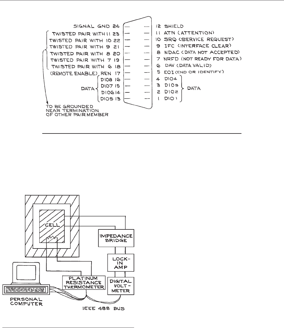
is shown in Figure 6.116. In this experiment, a digital
impedance bridge, lock-in amplifier, and digital voltmeter
are connected to a computer via an IEEE 488 bus. The
dielectric constant and conductivity of the liquid are cal-
culated from the measurement of the capacitance and
resistance of a liquid-filled cell. Measurements are made
over a range of temperatures, and a platinum resistance
thermometer is used to measure the thermostat tempera-
ture. Programming the IEEE 488 bus usually requires pro-
ficiency in a high-level language such as BASIC and
complete knowledge of the operation of each instrument
on the bus and its device-dependent commands. For the
system in Figure 6.116, timing is not a consideration and
the
measurement sequence can follow the simple flow
chart in Figure 6.117.
Implementing the flow chart with the IEEE 488 bus
requires knowledge of the characteristics of the instru-
ments on the bus. The thermomete r is a talker,andthe
digital voltmeter is a listener when its ranges are being
set, and a talker when sending the voltage readings to the
computer. To begin, the address of each instrument is set
with switches on their back panels. The instruments
are wired in daisy-chain fashion to the computer with
ribbon cable and the IEEE 488 piggyback plugs. Suffi-
cient time must be provided in the program for instrument
readings to stabilize. This is done with wait loops inserted
in the program (see Figure 6.118). The input and output
da
ta formats for each instrument must also be accommo-
dated in the program so that the commands and data
from the computer a re correctly read by the instruments,
and the data from the instruments correctly read and
Figure 6.115 IEEE 488 interface-bus connector pin assignment. Logic levels are TTL-
compatible negative logic (‘‘1’’, 0 to 0.4 V; ‘‘0’’, 2.5 to 5.0 V).
Figure 6.116 A personal-computer-controlled IEEE 488
temperature-measuring system.
DATA ACQUISITION 483
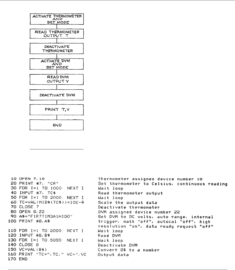
stored by the computer. Even for this relatively simple
system, the BASIC program requires several lines of
code. For more complex s ystems with special timing
requirements, simple BASIC pr ogra ms may be too s low
or too inflexible. When this is the case, systems with
separate software packages are required. Such systems
are offered by Keithley Instruments and National Instru-
ments, among others.
Data acquisition and control systems based on I/O mod-
ules and boards that connect directly to a personal com-
puter are justified when there are a large number of
standard sensors and the cost of separate IEEE 488 instru-
ments is too great. For an I/O board system, it is necessary
to consider the number of input channels, the number of
output channels, input and common-mode signal levels,
sampling rates, measurement precision, and computer
and software requirements.
9
Interface boards can be programmed directly in BASIC
once the addresses of all the I/O ports are known. As with
all dynamic systems, timing is crucial, and routines must
be written to allow time for ADC conversions and data
storage. Interpreted BASIC programs are slow, while com-
piled BASIC has a considerable speed advantage. Opti-
mum speed and ease of programming are usually
accomplished with software supplied by the manufacturers
specifically for their interface boards. Such software
Figure 6.117 Flow chart for
measurement sequence in
system of Figure 6.116
Figure 6.118 IEEE-488 BASIC program example.
484 ELECTRONICS

has machine language subroutines for initializing the
ports and reading and writing data. These routines are
designed to be easy to use and can generally be called
from within a BASIC program. The more sophisticated
manufacturer-supplied software is menu driven, with true
foreground – background computer operation and graphic
data display with full interfacing to standard spreadsheet
packages. Since much more time is spent with software
than hardware, it is important that the programming mate-
rials supplied by the manufacturer be clear, easy to use,
and well documented.
A typical small, commercial, data-acquisition interface
circuit is shown in Figure 6.119(a). The details of analog
input
circuits are shown in Figure 6.119(b). In this exam-
ple,
there are four single-ended or two differential analog
inputs, each connected to a S/H circuit and analog multi-
plexer. The output of the multiplexer is connected to a
unit-gain instrumentation amplifier, a programmable-gain
amplifier, and a second S/H circuit. The output of the
second S/H is connected to a 12-bit ADC through a
signal-conditioning network. The ADC output goes
to the internal interface bus. Boards of this type plug
directly into the expansion slot of a personal computer.
Connections to the input circuits are made through the
screw terminals on the board.
Sample and hold circuits capture the analog input sig-
nals and hold for a time sufficient for the ADC to convert
the analog signal to a binary output. The operation of the
S/H has already been discussed. Of particular importance
are the acquisition time, the aperture time, the decay time,
and the slew rate (the maximum large-signal change that
the S/H circuit can produce).
Input circuits can typically accommodate full-scale
input voltages from 20 mV to 10 V. The number of samples
per second is from 5000 to 10 000. With a 12-bit ADC, the
system has a maximum resolution of 1 part in 4000, or
0.025%. In practice, this resolution cannot be realized for
low-level input signals because of amplifier zero and gain
drifts, noise, common-mode error signals, and ADC non-
linearities. These must all be taken into account and an
error budget established when assessing the final accuracy
of the system.
Important analog output specifications for instrument
control are the resolution and the settling time required
to achieve the quoted resolution. Since the analog output
voltages are the input signals to other devices, output volt-
age and current ranges are important. The digital input and
output ports are usually 8-bits wide and operate with TTL
levels.
The primary concern when connecting sensors to a data-
acquisition system is elimination of noise. Noise can be
generated on the signal lines from magnetic fields, electric
fields, thermal gradients, friction, and improper grounding.
These noise sources can be controlled by proper choice of
input and output impedances and of lead-wire composi-
tion, length, shielding, and placement.
High output-impedance, current-source transducers are
less sensitive to magnetically induced noise than low
output-impedance, voltage-source transducers. It is impor-
tant to distinguish between ground and common (or return)
lines in transducer circuits. Ground lines do not normally
carry current, but return lines do. Return lines carry the
signal currents that complete the transducer circuit. Opera-
tional amplifiers normally have a single output terminal
and terminals for positive and negative power-supply vol-
tages. There is no separate common terminal, and the return
current must flow in the power-supply lines. For this rea-
son, it is important to bypass the power-supply leads with
large, high-frequency ceramic disk capacitors located as
close to the amplifier as possible.
When a return line is connected to ground at more than
one point in the circuit, it is possible to develop a voltage
across the line due to small dif ferences in ground potentials
and the finite resistance of the return line. Grounding the
signal return line at a single point in the circuit changes a
single-ended transducer configuration to differential,andany
difference in ground potentials appears as a common-mode
voltage. When it is impossible to avoid multiple grounds in a
system, an isolator can be used between the transducer and
the input to the data-acquisition circuit. Because there is no
galvanic connection across an isolator, potential differences
between grounds cannot result in current flo w.
Return lines should have the lowest possible inductance
and should overlap the signal lines as much as possible.
Shielded, twisted-pair cable is generally best for trans-
ducer connections. The shielding does not carry a current
and serves to reduce electric and magnetic noise pickup.
With twisted-pair cable, pickup is induced equally in both
wires and can be canceled by an amplifier with a differ-
ential input. Twisted-pair cables in several sizes and
DATA ACQUISITION 485
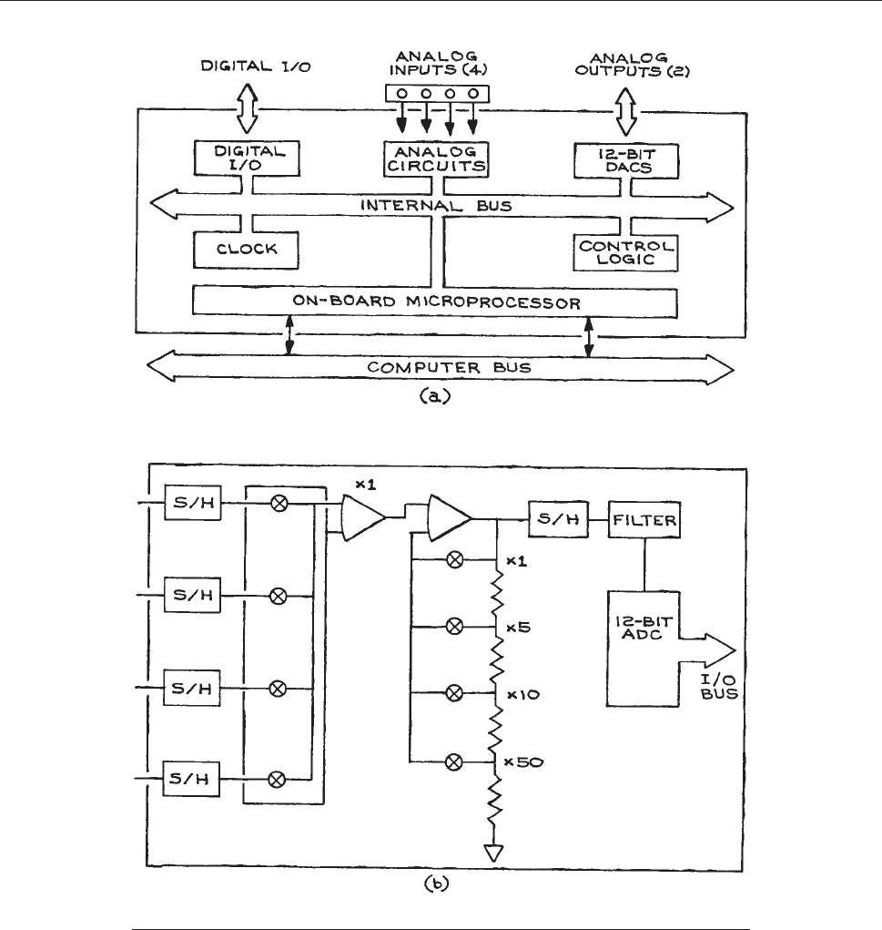
Figure 6.119 (a) Data-acquisition interface; (b) analog input circuits.
486 ELECTRONICS

configurations are available from Belden and Alpha.
Cable-length guidelines are given in Table 6.40. In coaxial
cable,
the outer conductor is the return line.
A s maller source of noise is static discharges when
insulators of dissimilar material s rub against each other.
This is called triboelectric induction and can be elimina-
ted with special low-noise cable that has graphite lubri-
cant between dielectric surfaces. The ultimate obstacle to
complete noise elimination comes from thermoelectric
effects when junctions of dissimilar m etals are a t differ-
ent temperatures. Typical values are 0.1 lV/°C. Thermo-
electric solder (70% cadmium, 30% tin) can be used
for low-level circui ts, and precautions should be taken
to keep all circuit elements and devices at the same
temperature. Carbon and metal-film resistors produce
larger thermoelectric voltages than precision wire-wound
resistors.
Once the sources of noise in the system have been
reduced to acceptable levels, input filtering can be used
to improve the signal-to-noise ratio. Filtering cannot, how-
ever, eliminate the effects of improper wiring.
Example of Sensor and Control Electronics. In
this example, a silicon substrate inside an ultrahigh vac-
uum chamber is heated to a predetermined temperature
and then maintained at that temperature while an electron
gun directs electrons at the surface and a mass spectrom-
eter monitors the masses of the atoms and molecules emit-
ted from the surface. An ion gauge monitors the pressure
in the experimental chamber. The data from the experi-
ment are count rates as a function of mass spectrometer
setting. The rates are recorded and stored for subsequent
analysis. A schemati c representation of the system is given
in Figure 6.120. The system is a mixed digital and analog
syst
em with a computer supplying control and data-acquis-
ition functions, and the heater and thermocouple circuits
operating with analog signals. D/A and A/D circuits pro-
vide the translation between the digital and analog
domains.
It is most convenient to divide the overall system into
subsystems and determine the operating conditions for
each of them. In the example, the subsystems are:
Substrate/heater
Thermocouple temperature monitor
DMM
Picoammeter current monitor
Mass spectrometer
Electron gun
Ion gauge
The substrate/heater and thermocouple temperature
monitor form the temperature control system that both
sends and receives signals to and from the computer. The
electron gun receives signals from the computer while the
DMM and ion gauge send signals. The mass spectrometer
both receives and sends signals. The signals it receives set
the mass range and scanning rate. The signals it sends are
pulses from the detector.
There are a number of manufacturers of computer inter-
face boards that are specifically designed for the control and
monitoring of experiments – among them are National
Instruments (manufacturer of LabVIEW), Hewlett-Packard
(Agilent), Keithley Instruments, and Datel. All have cata-
logs that describe their products in detail and provide very
useful information on the general configuration of data-
acquisition and control systems. The purpose here is to
provide a plan of organization and guidelines.
The first task is to define the operating parameters for
each of the subsystems. For the substrate/heater, this
means defining the input power necessary to obtain the
required temperature of the silicon substrate. Once the
power is known, it is possible to define the power-supply
requirements and its programming input requirements. For
this example, the heater is a coil of tungsten wire that has a
resistance of 3 X at room temperature. The required max-
imum power was determined to be 81 W (27 Vat 3 A). This
is supplied by a 300 W power supply with a range of 0 to
30 V at 0 to 10 A. The power supply is voltage program-
mable with variable gain, so that an input voltage from 0 to
Table 6.40 Instrumentation cable-length guidelines
Signal Bandwidth Accuracy Maximum Cable Length
a
Source (Hz) (%) (ft.) (m)
4 to 20 mA <10 0.5 1000–5000 300–500
61to610 V <10 0.5 50–300 15–90
610 mV to 61 V <10 0.5 5–100 1.5–30
a
Shielded twisted pairs.
DATA ACQUISITION 487

10 V will vary the output from 0 to 30 V when the internal
gain of the power supply is set to three. The outputs of D/A
cards used for power-supply control are generally 0 to 1
and 0 to 10 V. When this is not sufficient to drive the
output of the power supply to the required maximum
level, an intermediate gain stage will be required. The
supply that is used is current limiting. For this application,
the current-limiting control is set so that 3 A are available at
all voltage settings. This prevents excessive current draw
when the filament is cold – a necessary precaution for tung-
sten that has a temperature coefficient between 4.5 and 8.9 3
10
3
per °C.
Because the programming voltage to the heater power
supply is in the range 0 to 10 V, a computer interface card
with a DAC is used that has a maximum analo g outpu t
voltage of 10 V. The input to the card is a 12-bit code
giving a maximum possible resolution of one part in
4096 or 0.025% at 30 V output. At 27 V, the resolut ion
is 0.0225% slightly exceeding the maximum available
resolution. The the rmocouple is a type K NiCr/NiAl,
with a working temperatur e range of 200to1300°C.
It is non-magnetic and compatible with the ultrahigh vac-
uum environment in which it is located. The thermocou-
ple wires are crimped to a copper lug that is fixed to a stud
Figure 6.120 System for controlling the temperature of a silicon substrate while moni-
toring the atoms and molecules emitted from the surface under electron bombardment.
488 ELECTRONICS
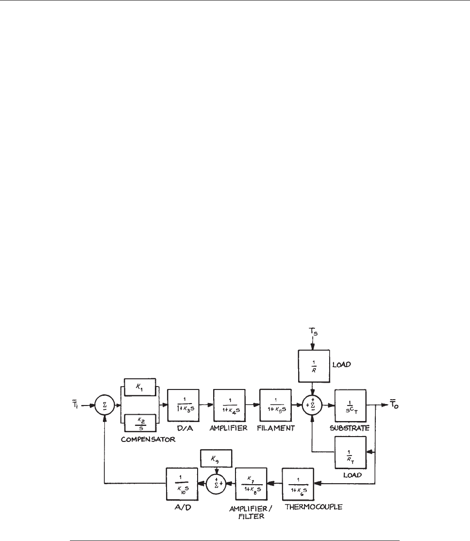
on the stage holding the silicon substrate. The wires are
connected to the leads of a UHV thermocouple electrical
feedthrough. The leads on the atmospheric pressure side of
the feedthrough are connec ted to the signal conditioner/
isolator unit that converts the output of the thermocouple
to an analog voltage that is changed to a temperature by the
software that interprets the outpu t from the interface card.
A block diagram of the substrate temperature control sys-
tem is shown in Figure 6.121. In this figure, the individual
functi
ons are represented by blocks. The Laplace trans-
form of the transfer function for each block is indicated
(see discussion of Laplace transforms in Section 6.1.5).
The
transforms are obtained from consideration of the
differential equations that relate the output of each func-
tion to the input. The compensator is a proportional/inte-
gral type with constants K
1
and K
2
adjusted to attain the
optimum response and stability of the circuit (see Section
6.7.8). One detail to b e noted is that the output power of
the
filament amplifier must be linearly related to the differ-
ence between the set temperat ure T
i
and the output temper-
ature T
o
for a Laplace transf orm analysis to be used.
Determination of Block Parameters. The time
response of the D/A, amplifier, filament, thermocouple,
amplifier/filter, and A/D are obtained from the specifica-
tions of the individual elements. The constants K
9
and K
10
were chosen so that the input to the A/D in the thermo-
couple circuit is 0 V at approximately 100 °C and 4 V at
1000 °C. For the system under consideration:
K
3
¼ 1.2 3 10
5
s
K
4
¼ 5 3 10
5
s
K
5
¼ 1 3 10
3
s
K
6
¼ 1 3 10
3
s
K
7
¼ 0.3535 V
K
8
¼ 86.67 s
K
9
¼ 0.25 s
K
10
¼ 1.2 3 10
5
s
The remaining parameters – thermal resistance, R
T
,
and heat capacity C
T
, are characteristic of the experimen-
tal arrangement and ar e determined experimentally fr om
heating and cooling curves and a measurement of the
maximum temperature at maximum power input. The
assumption is made that the heat loss from the s ubstrate
to the surroundings is proportional to the temperature
difference between the subs trate and s urroundings
(T
o
T
s
). The initial slope of the heating curve dT
o
=dt
(T
o
as a function of time for a constant heat input) when
the substrate is at the temperature of the surroundings
Figure 6.121 Block diagram of the silicon substrate-temperature-control system.
DATA ACQUISITION 489
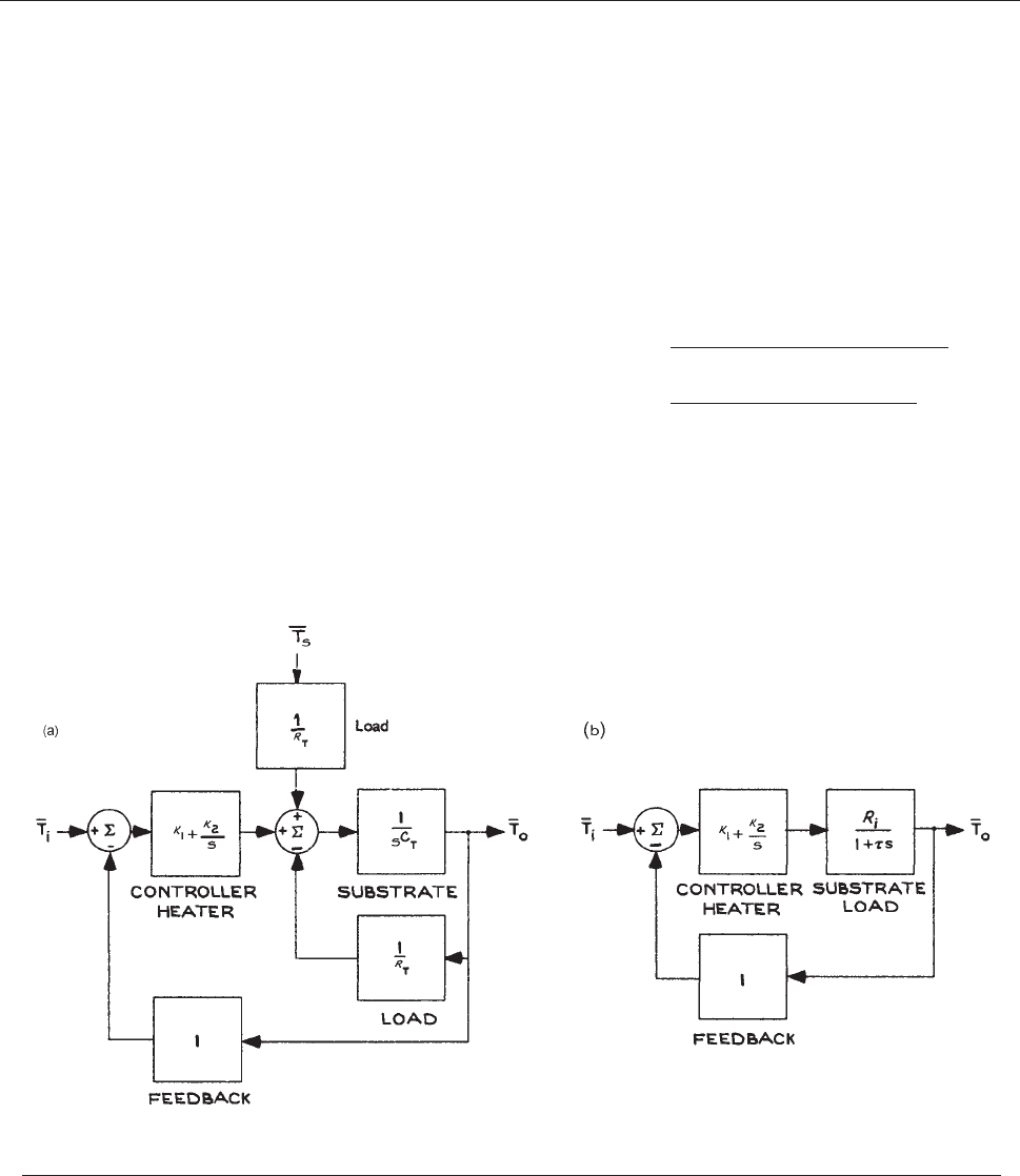
and the heat loss is zero is dT
o
=dt ¼ C
T
dQ=dt,whereC
T
is the heat capacity of the substrate and dQ=dt is the rate
at which heat is added to the substrate. Knowing dQ=dt,
the input power, and dT
o
=dt, C
T
can be calculated. R
T
is
correspondingly determined from the asymptotic temper-
ature of the substrate for a constant power input. Assuming
heat loss proportional to (T
o
T
s
), the thermal resistance
of the system R
T
is given by (T
o
T
s
)/input power. The
values of C
T
and R
T
can be checked by a cooling-curve
measurement. With the substrate initially at T
o
> T
s
and
no heat input, the time for the temperature to fall to e
1
of
(T
o
T
s
)isR
T
C
T
¼ 300 s. This is consistent with the
values for R
T
and C
T
of 5.6 K/W and 54 J/K.
Because the time constant for the substrate and load is
at least two orders of magnitude larger that any other
time constant in the system, it is possible to simplify
the circuit to the one shown in Figure 6.122(a),where
the
overall transfer function of the D/A, amplifier,
filament, and feedback transfe r function a re all set equal
to one. In Figure 6.122(b) , the substrate, load, and sum-
m
ing junction are replaced by a single transfer function
R
i
/(1 þ ss),whereR
i
is the effective thermal loa d equal
to R
T
þ T
s
/Q
i
.Inthiscase,s ¼ R
T
C
T
¼ 30 0 s, T
s
is the
temperature of the surroundings, and Q
i
is the power
input to the substrate at the set temperature T
o
. It should
be noted that the value of R
i
will change with the temper-
ature of the surroundings and the set temperature of t he
substrate. To maintain the substrate at 500 K, the system
requires a heat input of 36 W, giving a value of 13.9 K/W
for R
i
. T he overall transfer function for Figure 6.122(b),
T
o
ðsÞ=
T
i
ðsÞ,is
T
o
ðsÞ=
T
i
ðsÞ¼
13:9ðK
1
s þ K
2
Þ
300s
2
þð13:9K
1
þ 1Þs þ 13:9K
2
¼
as þ 1
21:6bs
2
þð0:072b þ aÞ s þ1
ð6:65Þ
where a ¼K
1
/K
2
and b ¼1/K
2
. The response and stabi lity
of the system are op timiz ed by the appropriate choice of
K
1
and K
2
. Figure 6.123 shows the frequency dependence
of the system transfer function for different values of a
and b. This can be done empirical ly or by using standard
Figure 6.122 (a) Simplified block diagram of the silicon substrate-temperature-control system; (b) block diagram with
load and substrate transfer functions combined.
490 ELECTRONICS
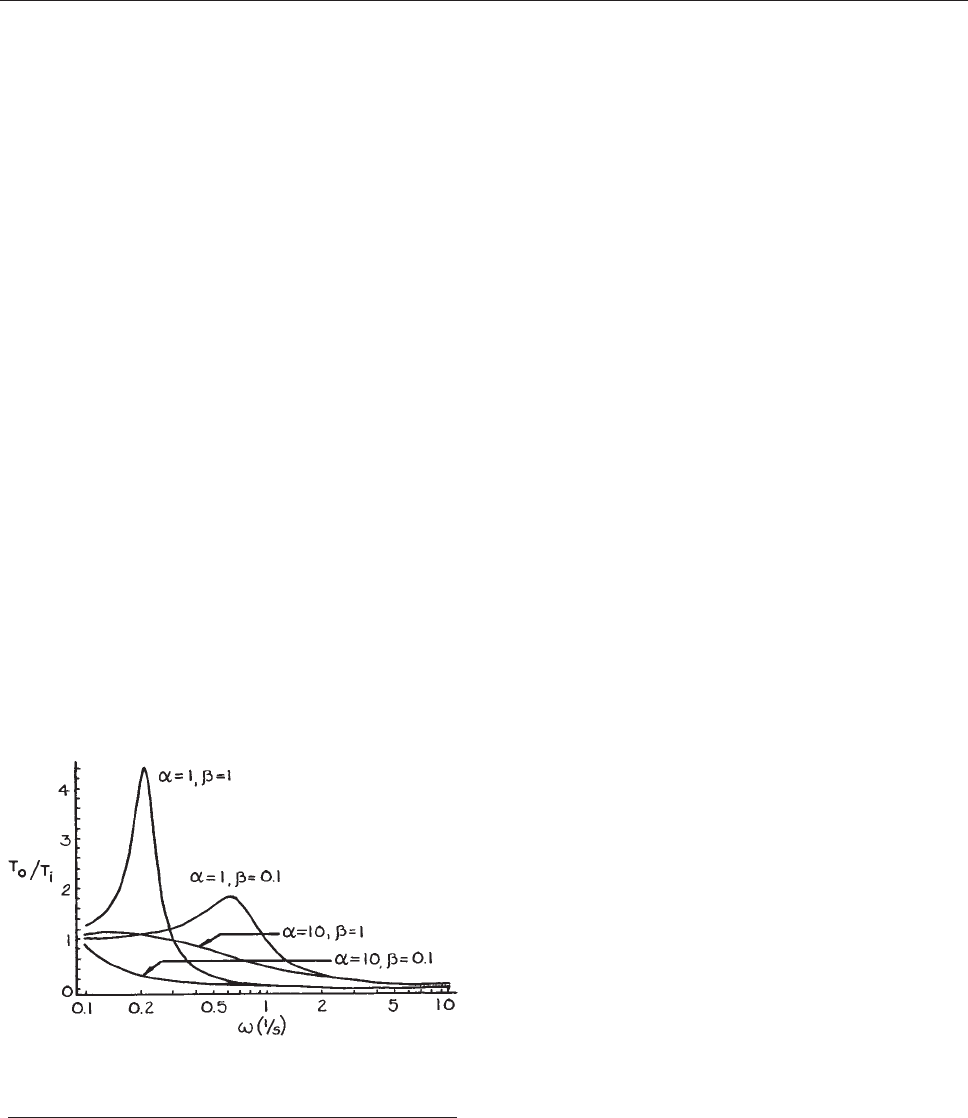
control analysis methods – some of which are discussed
in Section 6.7.8 and in more detail in the references at
the
end of the chapter. Programs such as Mathematica
TM
and Matlab
TM
have special packages for control analysis
and design.
A DMM card is used to monitor the voltage across the
leads of the heater and compare the results with the pro-
grammed voltage. The DMM is specified to have a reso-
lution of 5 1/2 digits 61 in the next to least significant
digit. When set on the 10 V range, the card can resolve
1 mV (0.01%) – more than adequate for verifying the out-
put voltage of the power supply considering that the max-
imum resolution of the DAC is only 0.025 %.
The AT-MIO-16X interface board from National Instru-
ments is supplied with software and connectors. It can be
installed in any available 16-bit expansion slot on a PC. It
has 16 single-ended and 8 differential analog input chan-
nels of 16 bits each, and a maximum sampling rate of 100
kilo-samples/s. Gains of 1, 2, 5, 10, 20, 50, and 100 are
software-selectable. The output of the ion gauge is con-
nected to one of the analog input channels. There are
two analog output channels driven by 16-bit DACs. The
two channels are used to control the electron-gun power
supply and mass spectrometer. The maximum update rate
is 100 kilo-samples/s and the output software-selectable
voltage ranges are 0 to 10 V unipolar, and 610 V bipolar.
The board also has eight digital TTL-compatible I/O lines
and three independent 16-bit counter/timers. One of the
counters is used to register the output counts from the mass
spectrometer. A standard GPIB interface board is used
to monitor the output of the picoammeter that registers
the current from the electron gun that is collected by the
silicon substrate.
6.8 EXTRACTION OF SIGNAL
FROM NOISE
6.8.1 Signal-to-Noise Ratio
With many experiments, an important consideration is the
minimum detectable signal that can be recovered. This
depends on the signal-to-noise ratio
10
(SNR or S/N) rather
than the absolute value of the signal. In counting experi-
ments, where the minimum signal is one event, the uncer-
tainty associated with C
s
signal counts is
ffiffiffiffiffi
C
s
p
so that the
relative uncertainty is
ffiffiffiffiffi
C
s
p
=C
s
or 1=
ffiffiffiffiffi
C
s
p
. In principle,
one could attain arbitrarily high precision by counting
for long times, but this is often not practical because of
instabilities in the experimental system.
With analog systems, where the signal is a voltage, cur-
rent, or charge, the SNR depends on the source resistance
and capacitance, shot noise, 1/f or flicker noise, and ampli-
fier noise. In this discussion, we assume that sources of
noise such as r.f.i. do not exist. The noise will be assumed
to be confined to the source and preamplifier and to repre-
sent the theoretical limit for such a combination.
Consider a detector that is a source of voltage with out-
put impedance R
S
, connected to an amplifier with a gain A
o
as shown in Figure 6.124. Johnson noise is associated with
the random motion of electrons in R
S
. Its rms value over a
frequency bandwidth Df in Hz is:
v
Johnson
¼
ffiffiffiffiffiffiffiffiffiffiffiffiffiffiffiffiffi
4kTR
s
Df
p
ð6:66Þ
where k is Boltzman’s constant (1.38 3 10
23
J/K), and T
is the absolute temperature of the resistor. Johnson noise is
frequency independent – that is, the rms noise per unit
bandwidth (noise density) is the same at all frequencies.
For this reason, Johnson noise is often called white noise.
For the purposes of circuit analysis, the noise from R
S
can
be represented by a voltage source giving a voltage v
Johnson
in series with a noiseless resistor R. The noise current from
this source is i
Johnson
¼ v
Johnson
/R.
Figure 6.123 Frequency dependence of steady-state
transfer functions for a range of system parameter values.
See text for definition of a and b.
EXTRACTION OF SIGNAL FROM NOISE 491
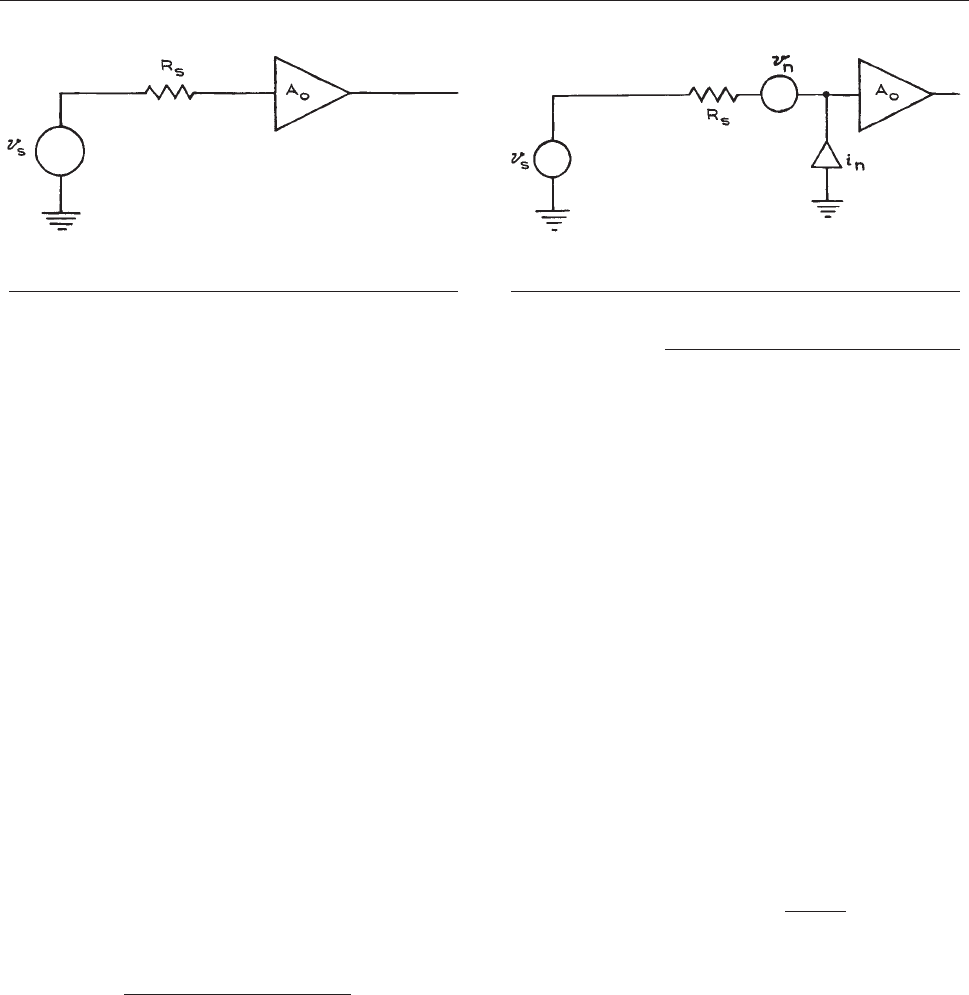
Shot noise has its origin in the discrete nature of the
electronic charge. The shot current noise accompanying
a current i is
i
shot
¼
ffiffiffiffiffiffiffiffiffiffiffiffi
2qiDf
p
ð6:67Þ
where q is the electronic charge in coulombs. Like Johnson
noise, shot noise is frequency independent.
Flicker or 1/f noise tends to dominate Johnson and shot
noise below 100 Hz. The frequency dependence of this
noise is of the form 1/f
n
, where n is usually between 0.9
and 1.35. Flicker noise imposes an important limitation on
the SNR at low frequencies. For this reason, measurements
should, if at all possible, be made at frequencies where
white noise dominates.
6.8.2 Optimizing the Signal-to-Noise Ratio
An ideal amplifier of gain A
o
can represent a real amplifier
with current and voltage noise generators at the input ter-
minals. It is usually assumed that the noise sources are
frequency independent. Consider the system in Figure
6.125, where v
n
and i
n
represent the rms voltage and cur-
rent noise per Hz
1/2
. The SNR is then the output voltage
due to the signal alone divided by the total output voltage,
including noise:
SNR ¼
v
s
ffiffiffiffiffiffiffiffiffiffiffiffiffiffiffiffiffiffiffiffiffiffiffiffiffiffiffiffiffiffiffiffiffiffiffiffiffiffiffiffiffi
4kTR
s
þ v
2
n
þði
n
R
s
Þ
2
q
ffiffiffiffiffiffi
Df
p
ð6:68Þ
From this formula it is clear that the SNR can be
improved by reducing R
S
, Df, and T. When characterizing
noise in an amplifier, the noise figure (NF) is often used:
NFðdBÞ¼20 log
10
input voltage SNR without amplifier
output SNR from amplifier
ð6:69Þ
An ideal amplifier will have the same SNR at both the
input and output terminals. The smallest possible NF is 0,
and an NF of 3 dB means that the amplifier has reduced the
SNR by 1=
ffiffiffi
2
p
at its output terminals from what it was at
the input terminals. Exceedingly good commercial ampli-
fiers can have NFs as low as 0.05 dB over a limited range of
frequency and source resistance. To evaluate the impor-
tance of the NF it is necessary to know the input signal
level, source resistance, and frequency bandwidth. If the
SNR is 10
3
at the input terminals of an amplifier, for
example, an amplifier with a NF of 20 dB will reduce it
to 10
2
at the output terminals. This may still be entirely
satisfactory for the intended application. Manufacturers of
preamplifiers and amplifiers often supply contour plots of
constant NF in frequency source-resistance space.
For optimum SNR, it is important to match the source
resistance to the amplifier. The optimum value of the
source resistor R
SO
is v
n
/i
n
. This results in a minimum
NF given by:
NF
min
¼ 10 log 1 þ
2v
2
n
4kTR
SO
ð6:70Þ
where R
SO
is the optimum value of the source resistance.
The source resistance is generally a property of the source.
To transform the source’s intrinsic resistance R
S
to the
optimum resistance R
SO
, a transformer is used (never an
additional series or shunt resistor). If the ratio of secondary
to primary turns is a then a
2
R
S
¼ R
SO
. Although it was
stated that the maximum SNR occurs when R
S
¼ 0, in
Figure 6.124 Voltage source v
s
with output impedance R
s
connected to an amplifier of gain A
o
.
Figure 6.125 Real amplifier and signal source v
s
with noise
sources represented by voltage and current sources v
n
and i
n
.
492 ELECTRONICS
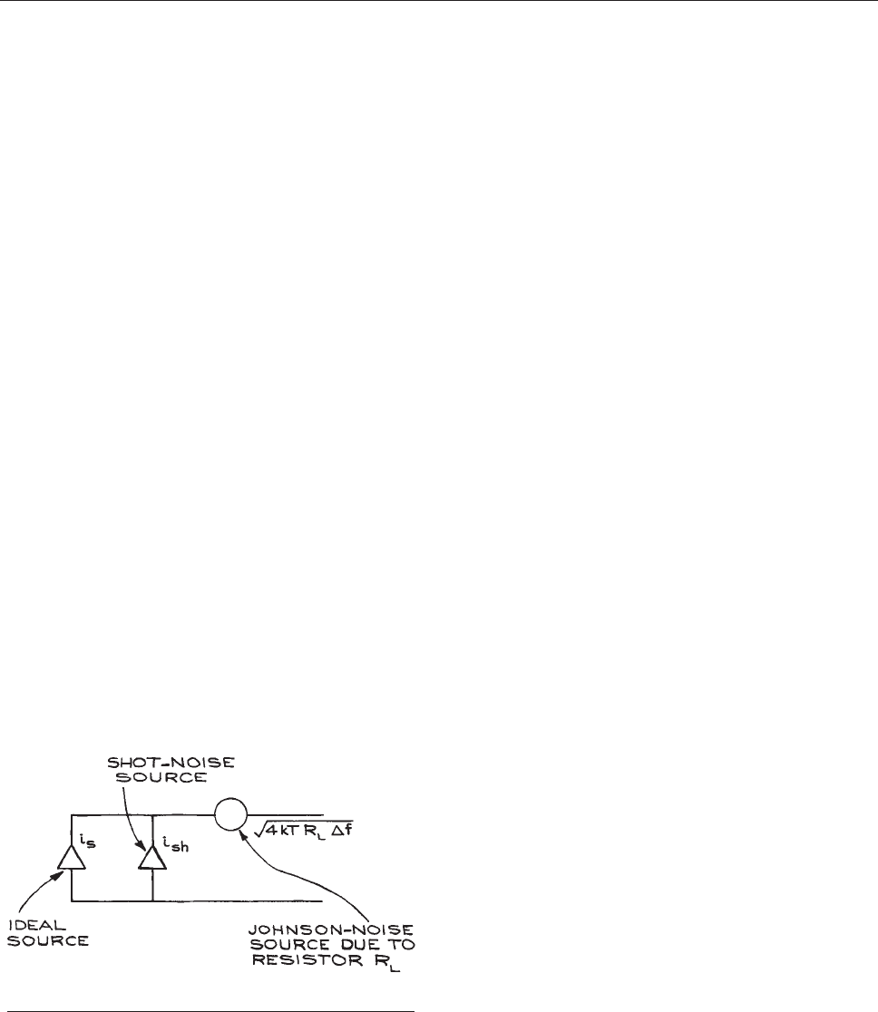
practice all sources have finite resistance and the SNR can
be optimized by transformer matching. Photomultiplier
tubes, photodiodes, and electron multipliers are best rep-
resented (see Figure 6.126) as noiseless constant-
current
sources in parallel with shot-noise and Johnson-
noise sources resulting from the addition of a load resistor,
R
L
, to the circuit. In this case the SNR is optimized by
using as large a value of R
L
as possible and an amplifier
with high input impedance and low v
n
and i
n
. Amplifiers
with FET input stages are the best choice. Maximum prac-
tical values of R
L
are limited by the capacitance C of the
input circuit (including cables) and the input impedance of
the amplifier. There is no benefit in having R
L
greater than
the input impedance of the amplifier or so large that the
time constant R
L
C requires working at low frequencies
where 1/f noise dominates. The justification for using large
values of R
L
comes from the fact that the voltage signal
from a current source is proportional to R
L
, while the
Johnson noise is proportional to
ffiffiffiffiffiffi
R
L
p
.
An alternative way of specifying amplifier performance
is with the equivalent noise temperature T
e
defined as the
necessary increase in temperature of the source resistor to
produce the observed noise at the amplifier output – the
amplifier being considered noiseless for this purpose:
T
e
¼ Tð10
NF=10
1Þ, ð6:71Þ
where T is the absolute temperature of the source resistor.
Using the example of the amplifier with an NF of 3 dB and
a source resistor at T ¼ 300 K:
T
e
¼ 300 Kð10
0:3
1Þ¼300 K ð6:72Þ
In this case, the amplifier introduces an amount of noise
equal to the noise from the source resistor.
6.8.3 The Lock-In Amplifier and Gated
Integrator or Boxcar
The proper matching of a signal source to an amplifier is
the first step to be taken in the recovery of a signal accom-
panied by noise. Once this has been done correctly, a
number of signal-enhancing techniques can be used to
extract the signal.
Because of the difficulty in making d.c. measurements
due to zero drifts, amplifier instabilities, and flicker noi se,
the signal of interest should, if at all possible, be at a
frequency sufficiently high that the dominant noise is
white noise. A d.c. or low-frequency signal can be con-
verted to a higher frequency by chopping the signal at the
higher frequency. It is essential to choose a chopper fre-
quency far from the power-line frequency and its harmon-
ics. Frequencies near known noise frequencies should be
avoided.
Signal-enhancing techniques are mainly bas ed on
bandwidth reduction. Because the white-noise power
per unit bandwidth is constant, reducing the bandwidth
will proportionally reduce t he noise power. Of course, as
the bandwidth goes to zero, the noise and signal power
both go to zero as well. Common bandwidth-narrowing
circuits are the resonant filter and low-pass filter. For
resonant filters, t he width of the re sonance is given in
terms of Q, which is approximately equal to f
0
/Df,where
f
0
is the frequency to which the filter is tuned and Df is the
filter bandwidth. Practical values of Q for el ectronic res-
onant filters vary from 10 to 100. A simple detection
system might take the form shown in Figure 6.127.The
rectifi
er converts the a.c. signal back to d.c., so it can
be recorded on a chart recorder or read from a meter.
With this arrangement, the noise passed by the filter is
rectified along with the signal and adds to the recorded
d.c. level.
The effective bandwidth can be substantially narrowed if,
in the above arrangement, the ordinary rectifier is replaced
by a synchronous rectifier. This kind of rectifier acts as a
switch that is opened and closed in synchronization with the
chopper. Because the phase relations for each of the noise
components are random (a characteristic of white noise),
Figure 6.126 Representation of noise sources in a detector.
EXTRACTION OF SIGNAL FROM NOISE 493
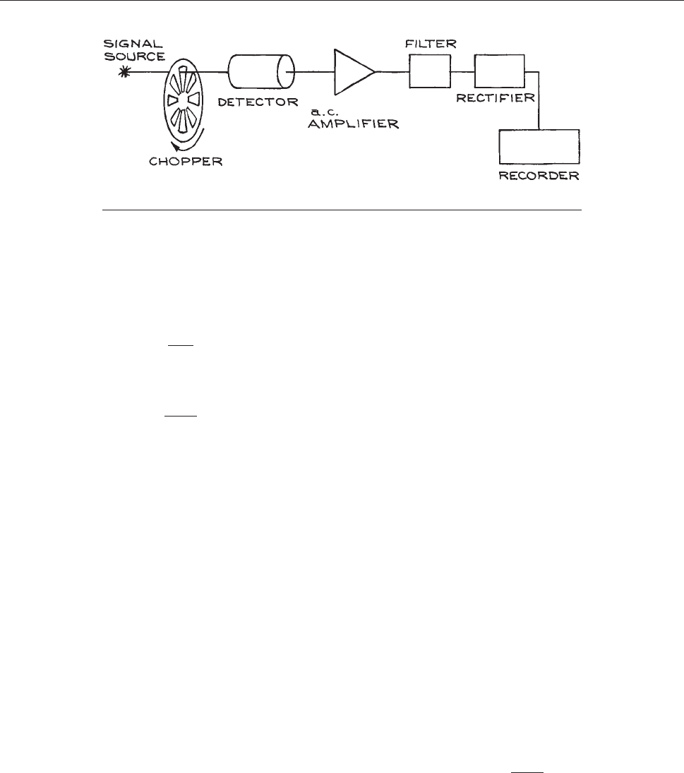
they will tend to cancel each other when averaged – a low-
pass filter at the output of the rectifier can be used to do the
averaging. The RC time constant of the filter is related to the
effecti ve pass band of the system Df by:
Df ¼
1
4RC
ð6:73Þ
for a single-section, low-pass filter, and
Df ¼
1
4nRC
ð6:74Þ
for n concatenated low-pass filters – each with time con-
stant RC. Quite small values of Df are possible with such a
system. The only limitation is the length of time necessary
for the measurement. If Df is the pass band, the measure-
ment time is approximately 1/Df so that it is necessary for
the source signal to remain stable over times comparable to
1/Df. The chopping frequency is normally chosen to be 10
times the highest component frequency to be recovered in
the source signal.
The system described above is often called a lock-in
amplifier or phase-sensitive detector. The details of the
operation of such devices are well documented.
11
As far
as signal enhancement is concerned, however, the formulae
given above are sufficient for estimating the benefits of
such devices. It is well to remember that the SNR is propor-
tional to 1=
ffiffiffiffiffiffi
Df
p
, so that narrowing the pass band by a factor
of four increases SNR by a factor of two, but increases the
time of measurement by a factor of four.
When the signal to be detected has the form of a repet-
itive low-duty-cycle train of pulses, the lock-in amplifier
may not be the best method for signal enhancement. The
duty cycle is the fraction of time during which the signal of
interest is present. With low duty cycles, signal informa-
tion is available for only a fraction of the total time, while
noise is always present. With timing and gating circuits, it
is possible to connect the signal line to an RC integrating
circuit only during those times when the signal is present.
The time constant of the integrator is then chosen to be
very much larger than the period of the pulse train. The
time required for the capacitor to charge to 99% of the final
voltage level is 4.6RC, so that five time constants after the
first gate opening the capacitor should be charged to within
1% of the final steady-state value – provided the signal is
continuously present. If the signal is present for a fraction c
of the time, the time constant of the integrator must be
increased to 5RC/c. With this system, known as a gated
or boxcar integrator, the SNR is increased only by increas-
ing the time of the measurement. The effective bandwidth
of the instrument is c/4RC. Table 6.41 compares the impor-
tant
parameters associated with lock-in amplifiers and
gated integrators.
6.8.4 Signal Averaging
With a repetitive signal, merely averaging the signal over
many cycles can improve the SNR. Let SNR
0
represent the
SNR in one cycle, and N the number of cycles over which
one averages. The SNR improvement is proportional to
ffiffiffiffi
N
p
. If each cycle lasts for a time s, the time T necessary
to arrive at a specified SNR is given by:
T ¼
SNR
0
SNR
2
s ð6:75Þ
Figure 6.127 Simple detection and signal-enhancement system.
494 ELECTRONICS

Lock-in amplifiers and gated integrators are inherently
superior to simple signal averaging because of the band-
narrowing functions they perform. The bandwidth
improvement is only an advantage, however, when the
highest frequency component in the signal to be recovered
permits a long integrating time.
6.8.5 Waveform Recovery
When it is necessary to know the variation of a signal with
time, waveform recovery techniques are needed. The gated
integrator can be converted to an instrument for waveform
recovery by the inclusion of variable delay and variable
gate-width functions. A separate RC network is required
for each delay time in such a scheme. A schematic repre-
sentation of such a system is shown in Figure 6.128. Each
separate
delay corresponds to a different part of the wave-
form. The duty cycle for each gate opening is s/T ¼ c,so
that the effective bandwidth is c/4RC. An integration time
of 5RC/c is needed for the charge on each capacitor to
reach a steady-state value. If the waveform has been
divided into n parts, the total time of measurement is
5nRC/c.
Digital schemes for recovering waveforms use ADCs to
convert the analog signal level to a digital number, which is
then recorded in the appropriate time channel with the aid
of delay and gating signals. With such instruments, called
digital signal analyzers, SNRs are only limited by the
length of time of the measurement. The long-term stability
of the various components, however, limits the use of very
long measuring times. If the absolute value of the waveform
is needed, one must record the number of cycles processed
by the instrument. Data rates are limited by the conversion
speed of the ADC that encodes the amplitude information.
An advantage of digital signal analysis is the increased
versatility in data manipulation and the production of per-
manent records on paper, magnetic, or semiconductor
media. Such data are then available for computer analysis.
Instruments related to the digital waveform recorders
are transient recorders and memory oscilloscopes. While
these offer no gain in SNR over that in the original signal,
they do provide outputs that are a record of a single wave-
form. An inefficient, but commonly used, method of SNR
enhancement with these instruments is the separate record-
ing of many waveforms and subsequent digital averaging
by a computer.
Table 6.41 Comparison of lock-in amplifier and gated integrator
Parameter Lock-in Amplifier Gated Integrator
Duty cycle, c > 0.50 < 0.50
Bandwidth, Df 1/8RC c/4RC
Minimum measurement time 5RC 5RC/c
Highest recoverable signal frequency f
max
1/20pRC for chopping frequency > pRC/2 c/20 pRC for repetition frequency > pRC/2
Design notes 1. Determine f
max
, the highest frequency
component of the signal to be recovered.
1. Required measurement time is 5RC/c.
2. Choose f
s
, the chopping frequency,
where f
s
¼10f
max
.
2. Bandwidth is c/4RC.
3. Choose low-pass filter constants 1/RC ¼
2pf, so as to pass frequency f
max
.
3. Preferred to a lock-in amplifier for signal
repletion rate < 10 Hz and low duty
cycle.
4. The bandwidth Df is 1/8RC, and a tuned
amplifier with a Q of 10 is sufficient to
pass all frequency components of the
signal to f
max
.
EXTRACTION OF SIGNAL FROM NOISE 495
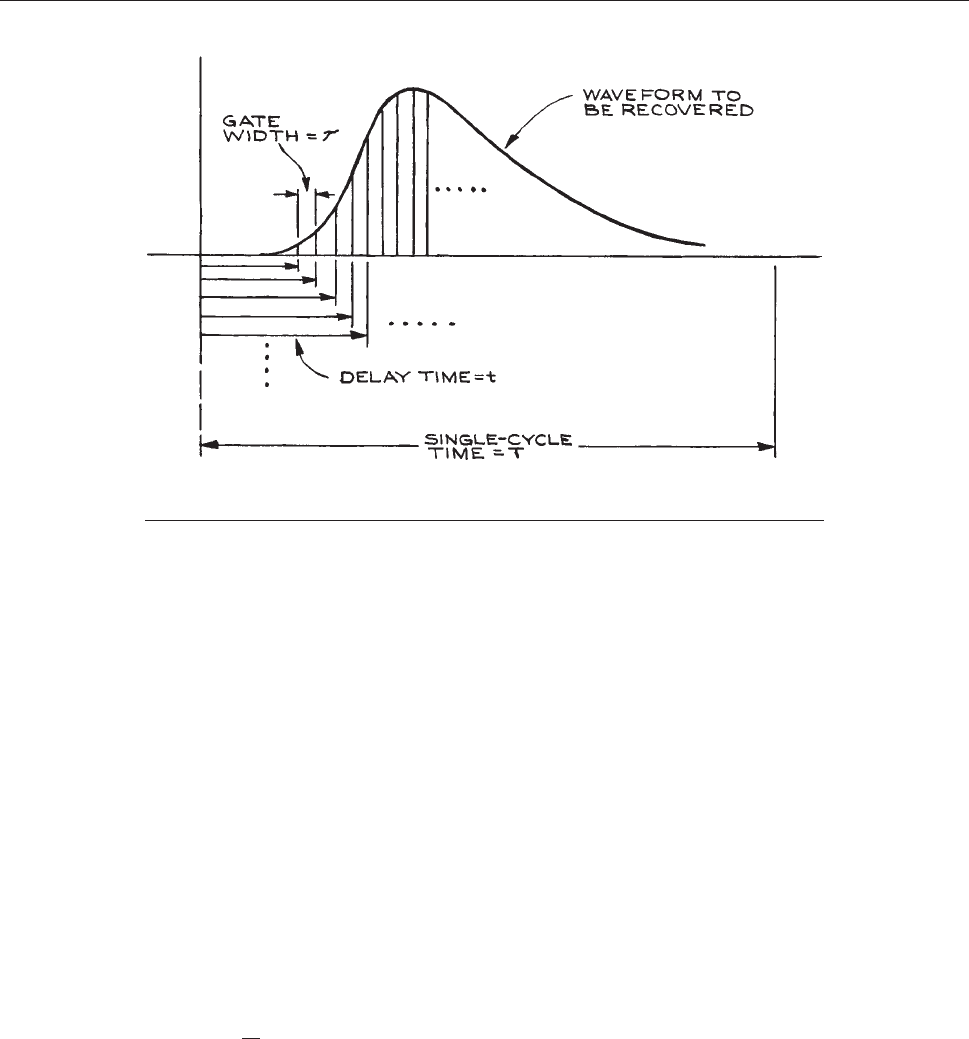
6.8.6 Coincidence and Time-Correlation
Techniques
There are a few general principles that govern all time-
correlation measurements, which will be discussed in suf-
ficient detail to be useful in assembling and optimizing the
operating parameters of experiments where time is a
parameter.
Correlated events are related in time, and this time rela-
tion can be established either with respect to an external
clock or to the events themselves. Random or uncorrelated
events bear no fixed time relation to each other but, on the
other hand, their very randomness allows them to be quan-
tified. Consider the passing of cars on a busy street. It is
possible to calculate the probability P
n
ðnÞ that n cars pass
within a given time interval in terms of the average number
of cars
n in the interval where P
n
ðnÞ, the Poisson distribu-
tion, is given by:
P
n
ðnÞ¼
n
n
n!
e
n
: ð6:76Þ
If 100 cars pass a fixed position on a highway in an hour,
for example, then the average number of cars per minute
is 100/60. The probability that two cars pass in a minute
isgivenby0:6
2
=2e
0:6
¼ 0:10. The probability that three
times the average number of cars pass per unit time is
0.02. P
n
ðnÞ and the integral of P
n
ðnÞ for
n ¼ 1 are shown
in Figure 6.129. It is worthwhile to note that only a
single
parameter, the average value
n, is sufficient to
define the function. The function is also not symmetric
about
n.
This example of passing cars has imp lications for
counting experiments. Consider again the particle-count-
ing experiment shown in Figure 6.72(a).Itconsistsofa
detector
, preamplifier, amplifier/shaper, discriminator,
and c ount er. The detector converts the energy of an
incoming particle to an electrical signal that is amplified
by the preampli fier to a level sufficient to be amplified
and shaped by the amplifier. T he discriminator converts
the signal from the amplifier to a standard electronic
pulse of fixed amplitude and time duration, provided that
the amplitude of the signal from the amplifier exceeds a
set thresho ld. Th e coun te r rec ords the number of puls es
from the disc rimina tor for a predet ermine d period of
time. The factors that affect themeasurementarecount-
ing rate, sign al d urati on, a nd processing times.
Figure 6.128 Relation between gate width s, delay time t, and single-cycle time T in
waveform recovery. The duty cycle c is given by s/T.
496 ELECTRONICS
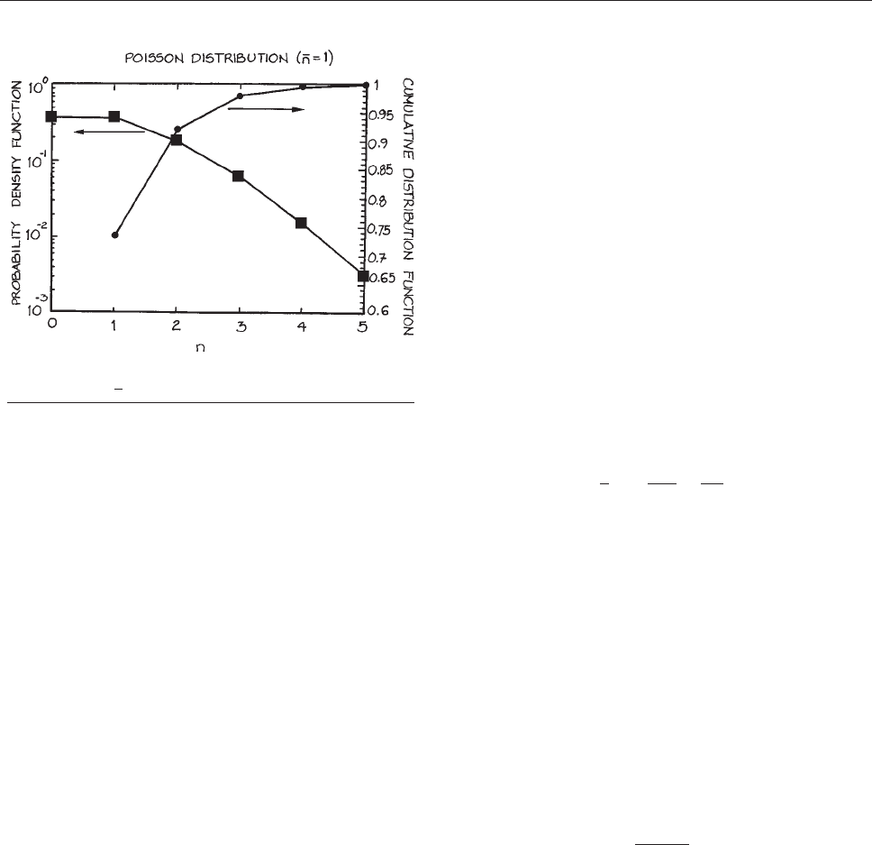
In counting experiments, the instantaneous rate at
which particles arrive at the detector can be significantly
different from the average rate . I n orde r to assess the rate
at which the s ystem ca n accept data, it is ne cessary to
know how the signals from the detector, preamplifier,
amplifier, and discriminator all vary with time. If signals
are arriving randomly at an average rate of 1 kHz at the
detector, for example, the average time between the start
of each signal is 1 0
3
s. If we consider a time interval of
10
3
s, the average number of signals arriving in that
interval is one. If as many as three pulses can be regis-
teredinthe10
3
s, then 99% of all pulses will be counted
(see Figure 6.129). To register the thr ee randomly dis-
trib
uted pulses in the 10
3
s interval, another factor of
three in time resolution is required, with the result that
the system must have the capability of registering events
at a 10 kHz uniform rate, in order to be able to register
randomly arriving events at a 1 kHz average rate with 99%
efficiency. For 99.9% efficiency, the required system band-
width increases to 100 kHz. Provided that the discriminator
and counter are capable of handling the rates, it is then
necessary to be sure that the duration of all of the electronic
signals are consistent with the required time resolution. For
1 kHz, 10 kHz and 100 kHz bandwidths, this means that the
signal durations must be no longer than 0.1, 0.01, and
0.001 ms, respectively. An excellent discussion of the
application of statistics to physics experiments is given
by Melissinos.
12
The processing times of the electronic units must also be
taken into consideration. There are propagation dela ys
associated with the active devices in the ele ctronics cir-
cuits and delays associated with the actual registering of
events by the counter. The manufacturers of counters spec-
ify proce ssing delays in terms of maximum count rate.
A 10 MHz counter may only count at a 10 MHz rate if
the input signals arrive at a uniform rate. For randomly
arriving signals with a 10 MHz average rate, a system with
a 100 MHz bandwidth is required, to record 99% of the
incoming events.
The result that is sought in counting experiments is a
rate (number of events per unit time). For convenience, we
divide the total time of the measurement T into n equal
time intervals, each of duration T/n. If there are N
i
counts
registered in interval i, then the mean or average rate is
given by:
1
n
+
n
i¼1
N
i
T=n
¼
N
N
T
ð6:77Þ
where N
N
is the total number of counts registered during
the course of the experiment. To assess the uncertainty in
the overall measured rate, we assume that the individual
rate measurements are statistically distributed about the
average value. In other words, they ari se from statistical
fluctuations in the a rrival times of the events and not
from uncertainti es introduced by the measuring instru-
ments. When the rate measurement is statistically dis-
tributed about the mean, the distribution of events can
be described by the Poisson distribution, P
n
ðnÞ.The
uncertaintyintherateisgivenbythestandarddeviation
andisequaltothesquarerootoftheaveragerate
ffiffiffi
n
p
.
Most significant is the relative uncertainty:
ffiffiffiffiffiffiffiffiffiffi
N= t
T
p
N= t
T
ð6:78Þ
The relative uncertainty decreases as the number of counts
per counting interval increases. For a fixed experimental
arrangement, increasing the time of the measurement
increases the number of counts. As can be seen from the
formula, the relative uncertainty can be made arbitrarily
small by lengthening the measurement time. Improvement
Figure 6.129 Poisson distribution and cumulative Poisson
distribution for
n ¼1.
EXTRACTION OF SIGNAL FROM NOISE 497
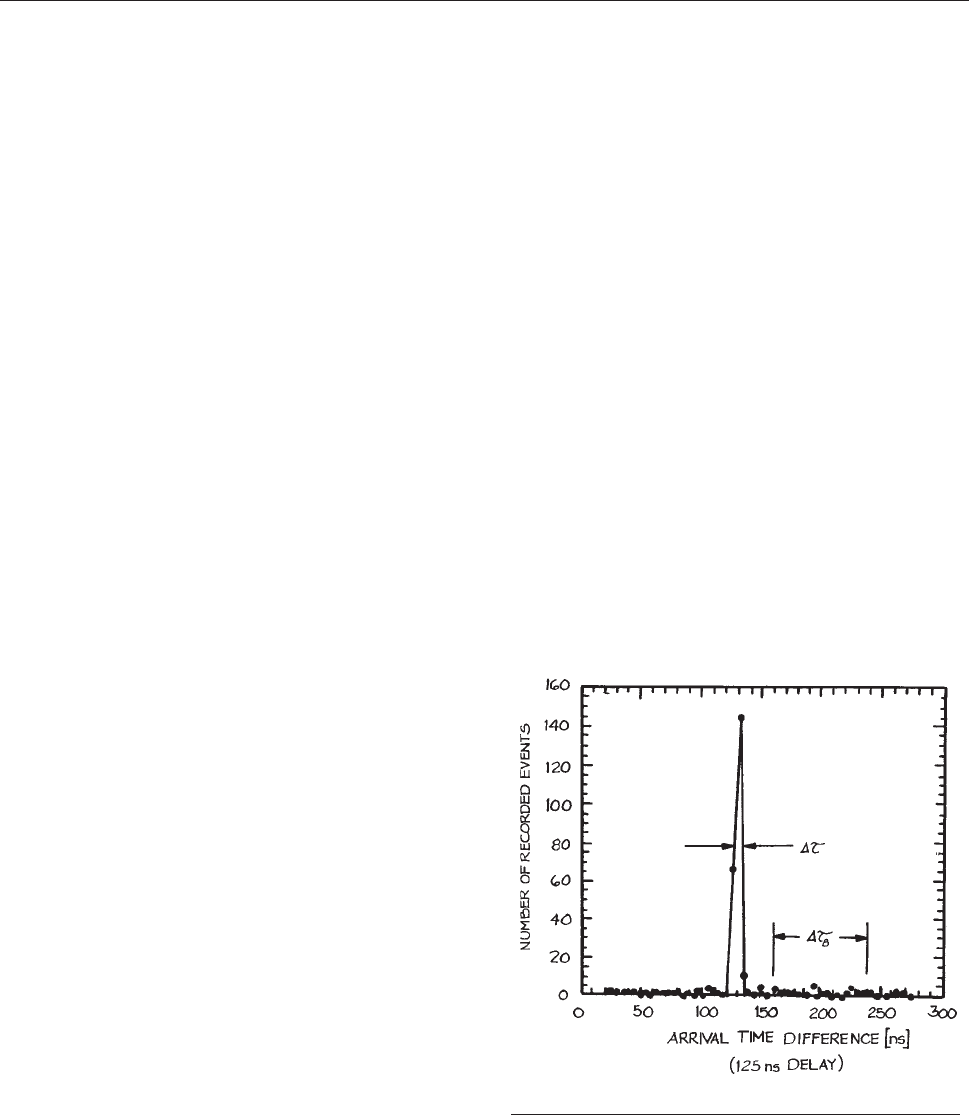
in relative uncertainty, however, is proportional to the
reciprocal of the square root of the measurement time.
To reduce the relative uncertainty by a factor of two, it is
necessary to increase the measurement time by a factor of
four. One soon reaches a point where the fractional
improvement in relative uncertainty requires a prohibi-
tively long measurement time.
Coincidence experiments require explicit knowledge of
the time correlation between two events. Consider the
example of electron impact ionization of an atom in which
a single incident electron strikes a target atom or molecule
and ejects an electron from it. Because the scattered and
ejected electrons arise from the same event, there is a time
correlation between their arrival times at the detectors.
In a two-detector coincidence experiment, of
which Figure 6.72(b) is an example, pulses from the
two
detectors are amplified andthensenttodiscrimina-
tors – the outputs of w hich are standard rectangular
pulses of constant amplitude and duration. The outputs
from the two discriminators are then sent to the start and
stop inputs of a time-to-amplitude converter or TAC.
Even though a single event is responsible for ejected
and scattered e lectrons, the two electrons will not arrive
at the detectors simultaneously because of differences in
path lengths and electron velocities. Electronic propa-
gation delays and cable delays also contribute to the
start and stop signals not arriving at the inputs of the
TAC simultaneously – sometimes the start signal arrives
first, sometimes the stop signal is first. I f the signal to the
start input arrives after the signal to the stop,thatpairof
events will not result in a TAC output. The result can be
a 50% reduction in the nu mber of recorded coinciden-
ces. To overcome this limitation, a time delay is inserted
in the stop line between the discriminator and the TAC.
This delay can be a length of coaxial cable (typical
delays are of the order of 1 ns/ft. – see Table 6.11), a
lumped
delay line, or an electronic delay circuit. The
purpose of the delay is to insure that the stop signal
always arrives at the stop input of the TAC after the start
signal. A perfect coincidence will be recorded at a time
difference approximately equal to the de lay time. When
a time window twice the length of the delay time is used,
perfect coincidence will lie at the center of the time
window, and it is possible to make an accurate assess-
ment of the ba ckground by considering the regions to
either side of the perfect coincidence region. An exam-
ple of a time spectrum is shown in Figure 6 .130.
An
alternative to the TAC and PHA/ADC (see Section
6.4.6) is the time-to-digital converter (TDC) – a unit that
combines the functions of the TAC and PHA/ADC. These
units have start and stop inputs and an output that provides
a binary number with a value that is directly proportional
to the time difference between the stop and start signals.
The TDC can be connected to an MCA or PC with the
appropriate digital interface.
By storing the binary outputs of a PHA/ADC or a TDC
in the form of a histogram in the memory of a MCA or PC,
analyses can be performed on the data taking full account
of the limitations of the individual components of the
measuring system. For the preamplifiers and discrimina-
tors, time resolution is the principal consideration. For the
TAC, resolution and processing time can be critical. The
PHA/ADC or TDC provide the link between the analog
circuits of the preamplifiers and discriminators and the
digital input of the MCA or PC. The conversion from
analog to digital by a PHA/ADC or TDC is not perfectly
linear and the deviations from linearity need to be taken
into consideration in precise work.
To assess the precision of a coincidence measurement,
it is necessary to consider, not just the event under
Figure 6.130 Coincidence time spectrum.
498 ELECTRONICS

consideration, but also all other events arriving at th e two
detectors. While the events under study are correlated in
time and result in a peak in the time spectrum centered
approximately at the dela y time, the re are also back-
ground events that be ar no fixed time relation to each
other. If the average ra te of the backgroun d events in
each detector is R
1
and R
2
, t hen the rate that two such
events will be recorded within time Ds is given by: R
B
,
where:
R
B
¼ R
1
R
2
Ds ð6:79Þ
Let the rate of the event under study be R
A
. It will be
proportional to the probability of occurrence of the event
p
A
, the source function S, and the acceptances and efficien-
cies of the detectors d
1
and d
2
:
R
A
¼ p
A
Sd
1
d
2
ð6:80Þ
For the background, each of the rates R
1
and R
2
will be
proportional to the source function, the probability for
single events p
1
and p
2
, and the properties of the individual
detectors:
R
1
¼ Sp
1
d
1
R
2
¼ Sp
2
d
2
ð6:81Þ
Combining the two expressions for R
1
and R
2
:
R
B
¼ S
2
p
1
p
2
d
1
d
2
Ds ð6:82Þ
Comparing the expressions for the background rate and
the signal rate, one sees that the background increases as
the square of the source function while the signal rate is
proportional to the source function. The signal-to-back-
ground rate R
AB
is then:
R
AB
¼
p
A
p
1
p
2
1
SDs
ð6:83Þ
It is important to note that the signal is always accompa-
nied by back grou nd. We now consider the signal and
background after accumulating counts over a time T.
For this, it is informative to refer to the t ime spectrum
in Figure 6.130. The total number of counts within an
ar
rival time difference Ds is N
T
and t his number is the
sum of the signal counts N
A
¼ R
A
T a nd the ba ck gr oun d
counts N
B
¼ R
B
T :
N
T
¼ N
A
þ N
B
ð6:84Þ
The determination of the background counts must come
from an independent measurement, typically made in a
region of the time spectrum outside of the signal region,
yet representative of the background within the signal
region. The uncertainty in the determination of the signal
counts dN
A
is given by the square root of the uncertainties
in the total counts and the background counts:
dN
A
¼
ffiffiffiffiffiffiffiffiffiffiffiffiffiffiffiffiffiffi
N
T
þ N
B
p
ð6:85Þ
The essential quantity is the relative uncertainty in the
signal counts dN
A
=N
A
. This is given by:
dN
A
=N
A
¼
ffiffiffiffiffiffiffiffiffiffiffiffiffiffiffiffiffiffi
N
T
þ N
B
p
=N
A
¼
ffiffiffiffiffiffiffiffiffiffiffiffiffiffiffiffiffiffiffiffiffi
N
A
þ 2N
B
p
=N
A
¼
ffiffiffiffiffiffiffiffiffiffiffiffiffiffiffiffiffiffiffiffiffiffiffiffiffiffi
R
A
T þ 2R
B
T
p
=R
A
T
¼
ffiffiffiffiffiffiffiffiffiffiffiffiffiffiffiffiffiffiffiffiffi
1 þ 2=R
AB
R
A
T
s
ð6:86Þ
Expressing R
A
in terms of R
AB
results in the following
formula:
dN
A
=N
A
¼
ffiffiffiffiffiffiffiffiffiffiffiffiffiffiffiffiffiffiffiffiffiffiffiffiffiffi
R
AB
þ 2ðÞDs
p
2
A
p
1
p
2
d
1
d
2
T
v
u
u
u
t
ð6:87Þ
There are a number of conclusions to be drawn from the
above formula. The relative uncertainty can be reduced to
an arbitrarily small value by increasing T, but because the
relative uncertainly is proportional to 1=
ffiffiffiffi
T
p
, a reduction in
relative uncertainly by a factor of two requires a factor of
four increase in collection time. Reducing Ds can also
reduce the relative uncertainty. It is understood that Ds is
the smallest time window that includes the entire signal.
Using the fastest possible detectors, preamplifiers, and dis-
criminators and minimizing time dispersion in the section
of the experiment ahead of the detectors all help to
decrease Ds.
The signal and background rates are not independent,
but are coupled through the source function S.Asa
EXTRACTION OF SIGNAL FROM NOISE 499

consequence, the relative uncertainty in the signal
decreases with the signal-to-background rate R
AB
, a some-
what unanticipated result. Dividing dN
A
=N
A
by its value
at R
AB
¼ 1 gives a reduced relative uncertainty
dN
A
=N
AB
½
R
equal to
ffiffiffiffiffiffiffiffiffiffiffiffiffiffiffiffiffiffiffiffiffiffiffiffiffi
R
AB
þ 2ðÞ=3
p
. To review this
result, consider a case where there is one signal count
and one background count in the time window Ds. The
signal-to background ratio is 1, and the relative uncertainty
in the signal is
ffiffiffiffiffiffiffiffiffiffiffi
2 þ 1
p
=1 ¼ 1:7. By increasing the source
strength by a factor of ten, the signal will be increased by a
factor of 10 and the background by a factor of 100. The
signal-to-background ratio is now 0.1, but the relative
uncertainty in the signal is
ffiffiffiffiffiffiffiffiffiffiffiffiffiffiffiffiffiffiffiffiffi
110 þ 100
p
=10 ¼ 1:45 – a
clear improvement over the larger signal-to-background
case.
Another method for reducing t he relative uncertainty
is to increase the precision of the measurement of back-
ground. The above formulae are based on an independ-
ent measurement of background over a time window Ds
that is equivalent to the time window within which the
signal appears. If a larger time w indow for the back-
ground is used, the uncertainty in the background deter-
mination can be correspondingly reduced. Le t a time
window of width Ds
B
be used for the determination
of background, where Ds=Ds
B
¼ q <1. If the rate at
which counts are accumulated in time window Ds
B
is
R
BB
, the background counts to be sub tracted from
the total counts in time window dN
A
/ N
A
become
qR
BB
T ¼ qN
BB
. The uncertainty in the number o f b ack-
ground counts t o be subtracted from the total of signal
plus background is
ffiffiffiffiffiffiffiffiffiffiffiffiffiffi
q
2
N
BB
p
. The relative uncertainty
of the signal is then:
ffiffiffiffiffiffiffiffiffiffiffiffiffiffiffiffiffiffiffiffiffiffiffiffiffiffiffiffiffiffiffiffi
1 þ 2q
2
N
BB
=N
A
N
A
s
¼
ffiffiffiffiffiffiffiffiffiffiffiffiffiffiffiffiffiffiffiffiffiffiffiffiffiffiffiffi
1 þ 2qN
B
=N
A
N
A
s
ð6:88Þ
The expression for the reduced relative uncertainty is
then:
dN
A
=N
AB
½
R
¼
ffiffiffiffiffiffiffiffiffiffiffiffiffiffiffiffiffiffiffiffiffiffiffi
R
AB
þ 2qðÞ
3
r
ð6:89Þ
The single coincidence measurement can be expanded to a
multiple detector arrangement if it is necessary to measure
coincidence rates as a function of more than one parame-
ter. This is a much more efficient way of collecting data
than having two detectors that are scanned over the range of
the parameters. Depending on the signal and background
rates, detector outputs can be multiplexed and a detector
encoding circuit can be used to identify those detectors
responsible for each coincidence signal. If detectors are
multiplexed, it is essential to recognize that the overall
count rate is the sum of the rates for all of the detectors.
This can be an important consideration when rates become
comparable to the reciprocal of system dead time.
It is often the case that signal rates are limited by the
processing electronics. Consider a coincidence time spec-
trum of 100 channels covering 100 ns with a coincidence
time window of 10 ns. Assume a signal rate of 1 Hz and a
background rate of 1 Hz within the 10 ns window. This
background rate implies an uncorrelated event rate of 10
kHz in each of the detectors. To register 99% of the incom-
ing events, the dead time of the system can be no larger
than 10 ls. The dead time limitation can be substantially
reduced with a preprocessing circuit that only accepts
events falling within 100 ns of each other (the width of
the time spectrum). One way to accomplish this is with a
circuit that incorporates delays and gates to only pass sig-
nals that fall within a 100 ns time window. With this circuit
the number of background events that need to be processed
each second is reduced from 10, 000 to 10, and dead times
as long as 10 ms can be accommodated while maintaining
a collection efficiency of 99%. This can be considered to
be an extension of the multiparameter processing in which
the parameter is the time difference between processed
events. Goruganthu et al. discuss a preprocessing circuit.
13
6.9 GROUNDS AND GROUNDING
6.9.1 Electrical Grounds and Safety
A battery or power supply produces a potential difference
between its two output terminals. Only by defining the
potential of one of the terminals in an absolute way can
the potential of the other terminal be given an absolute
value. By convention, the electrical potential of the earth
is defined to be zero. When one output terminal of a battery
or power supply is connected to the earth, the absolute
potential of the other terminal is then equal to the potential
500 ELECTRONICS

difference. Because the surface of the earth is a fairly good
conductor of electricity, all points will be at nearly the
same potential. A good connection to the earth via a copper
rod buried in the ground is the most convenient way of
establishing zero potential. Since such connections are not
always readily available in the laboratory, one often uses
connections to metal water pipes that go underground, to
define zero potential.
Most connections to the a.c. line are now made with
three-prong plugs and three-conductor wire. The wire is
usually color coded in North America – black correspond-
ing to the high-voltage or hot side of the line, white to the
low-voltage or neutral, and green to the earth or ground.
The terminals on a.c. plugs and receptacles are also coded –
the hot terminal is brass, the neutral terminal is chrome-
plated, and the ground terminal is dyed green. Switches
and fuses for use with a.c. lines should always be placed in
the hot line, otherwise the full line voltage will be present
at the input even with an open switch or a blown fuse.
The three-wire system is designed for safety. Consider a
piece of electrical equipment with a metal case operating
from the a.c. line. Normal practice requires that the case be
connected to the green ground wire of the line cord. Should
the hot wire come in contact with the case, a very large
current would flow in the hot line and blow a fuse or open a
circuit breaker. If the case is not connected to ground, it
will assume the potential of the hot line and could give an
electric shock to anyone touching it. Of course, if the case
were not a conductor, there would be no danger even if the
hot line made a connection to it. There are a large number
of appliances and hand power tools with so-called double
insulated cases that do not require a separate ground con-
nection for safety purposes. Ground-fault (circuit) inter-
rupters (GFI or GFCI) are safety devices that are
incorporated in a.c. power outlets where there is a danger
of operators of electrical equipment attached to the outlet
touching electrical ground while using the equipment. The
GFI senses any current flowing directly to ground and
switches off all power to the equipment to minimize elec-
trical shock. Ground-fault interrupter electrical outlets are
standard in humid environments outdoors and in bath-
rooms and underground installations.
From this discussion it should be clear that fuses and
circuit breakers are important safety elements in electrical
circuits. Fuses are generally of either the standard quick-
response type or the slow-blow type. The former will open
whenever its maximum rated current is exceeded, even
momentarily, while the slow-blow fuse is designed to sus-
tain momentary current surges in excess of the maximum
rated continuous value. The two types are not interchange-
able, even though they may have identical maximum con-
tinuous current ratings. Circuit breakers are generally of
the electromagnetic-relay or the bimetallic-strip type.
They can be reset after opening from an overload.
It is sometimes necessary to float or remove all ground
connections from a piece of electrical equipment. This is
necessary when a signal between two points in a circuit,
neither of which is at ground, is to be measured, amplified,
or processed in some way. Power supplies are floated when
it is necessary to produce a well-defined potential difference
with reference to a nonzero potential. An example is the
filament heater supply of a high-voltage electron gun with
the filament at a high negative potential. The heater supply
is connected across the filament with one lead at the high
negative potential. In this configuration, neither heater sup-
ply lead is at ground potential. Floating introduces the pos-
sibility of additional noise and electrical breakdown within
the circuit with a resulting destruction of components. There
are safety hazards associated with floated circuits.
At this point it is worthwhile to make the distinction
between d.c. and a.c. grounds. A d.c. ground connection
is a direct low-resistance connection to ground, while an
a.c. ground connection is one that does not permit d.c.
currents to flow while offering low impedance to a.c. cur-
rents. In
Figure 6.131, power supply 1 has the negative
terminal
and case (G terminal ) at d.c. ground. Power
Figure 6.131 Power supply 2 floating on power supply 1.
The V2
+
,V2
, and G terminals of supply 2 are assumed to
have no direct d.c. connection to ground.
GROUNDS AND GROUNDING 501
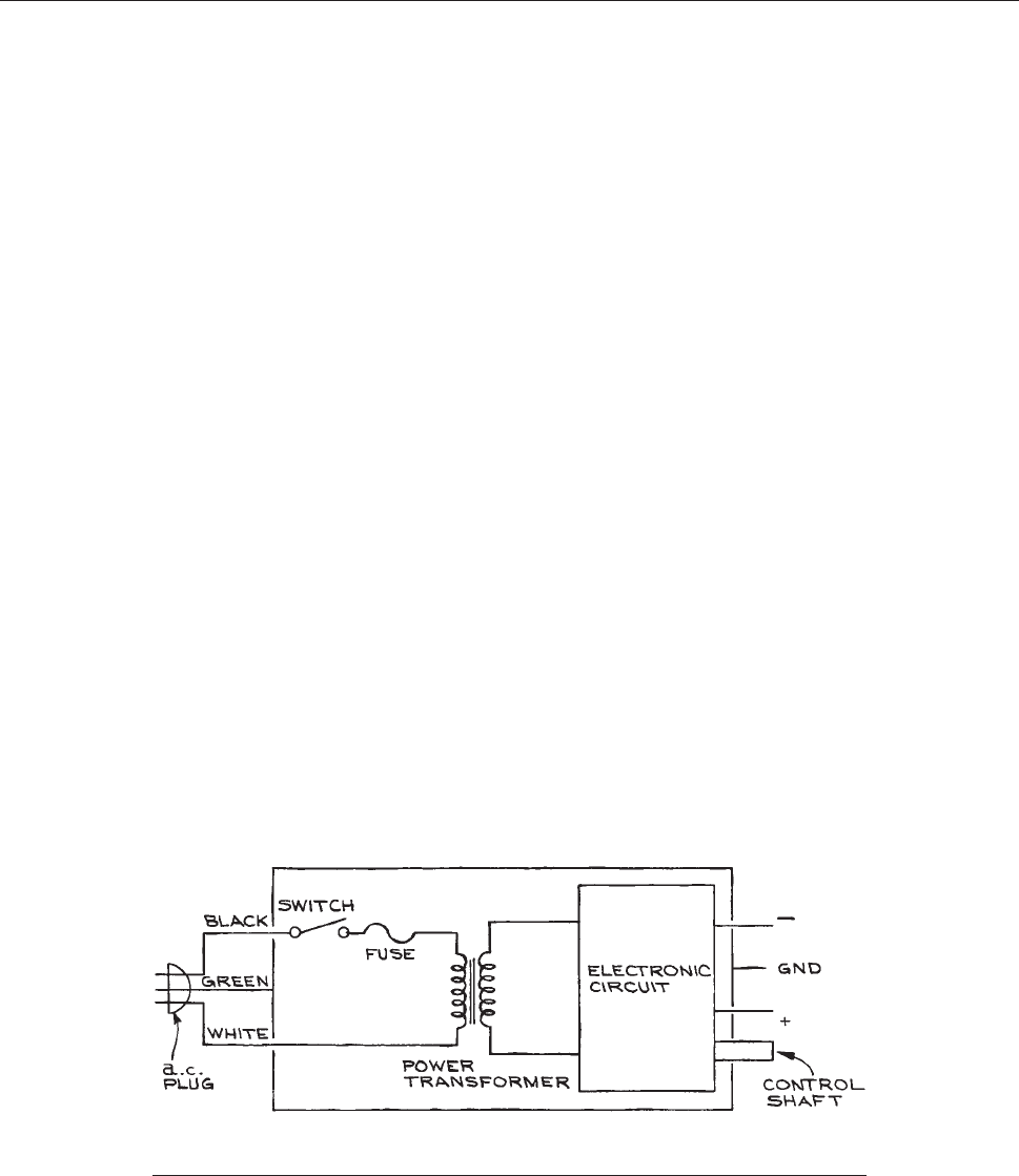
supply 2 is floating on power supply 1 and, in the absence
of any external connections, no current will flow through
the terminals of the supplies. Since high-quality power
supplies generally have very low output impedances, the
a.c. impedances of the terminals marked V1
+
,V2
, and
V2
+
with respect to ground are low, although the potentials
at the terminals are not zero. It is good to keep in mind that
the impedances to ground are frequency-dependent
because of the characteristics of the output circuits. At high
frequencies, the impedances may become large due to the
frequency characteristics of the output circuit. As a result,
transient voltage spikes may not be effectively shunted to
ground and may adversely affect the circuits to which the
power supplies are connected. A remedy is the use of good
high-frequency capacitors of an adequate voltage rating
between the terminals V1
+
and V2
+
and ground.
Figure 6.132 illustrates a typical line-operated power
supply
connected to an a.c. outlet via a three-wire line
cord. Under normal operation, either the negative or the
positive output terminal is connected to the ground termi-
nal, depending on whether a positive or a negative voltage
with respect to ground is desired. When floating the power
supply, the ground connection is removed and the potential
at which the supply is to be floated is applied to either the
positive or negative output terminal. This may be satisfac-
tory for levels of as much as a few hundred volts, but has its
hazards because the internal circuitry is floating, while the
case is at ground through the green wire in the three-wire
line plug. Potentials at least equal to the floating potential
plus the potential difference at the output terminals now
exist at the terminals of several components in the internal
circuit. Components are often mechanically fixed to the
grounded chassis. The electrical insulation between the
components and the chassis, as well as that between
the primary and secondary of the power transformer, must
be sufficient to sustain the d.c. voltage difference. In the
event of electrical breakdown, components will be des-
troyed and the shafts of the controls may attain a potential
that is equal to the floating potential and thus present a
shock hazard. The maximum potential for floating line-
powered equipment in this way is generally 600 V.
When floating line-operat ed equipment at voltages
above the rated maximum voltages, it is necessary to
completely remove the ground connection to the case .
The easiest method is to use a two-terminal to three-
terminal a.c. line-plug converter and not connect the third
terminal to ground at the a.c. outlet. If the case of t he
instrument is then electrically isolated from all conduct-
ing surfaces by placing it in a P lexiglasÔ enclosure, it
can b e electrically floated at the desired potential without
risk of electr ical breakdown be twe en the components of
the circuit and the case. With the case at a nonzero poten-
tial, there is a shock hazard associated with cont act ing it
and the controls so that ac cess must be provided via aux-
iliary insulated knobs and shafts. A further potential
problem is the possibility of electrical breakdown
between the primary and secondary windings of the
power transformer. At the primary, the peak voltage val-
ues are +155 V, corresponding to the normal peak values
of the a.c. line voltage. The secondary voltage, however,
will have a d.c. compone nt equal to the floating voltage
superimposed on the normal a.c . value. If the resulting
Figure 6.132 Mounting a line-operated power supply so that both output terminals are
independent of the a.c. line ground.
502 ELECTRONICS
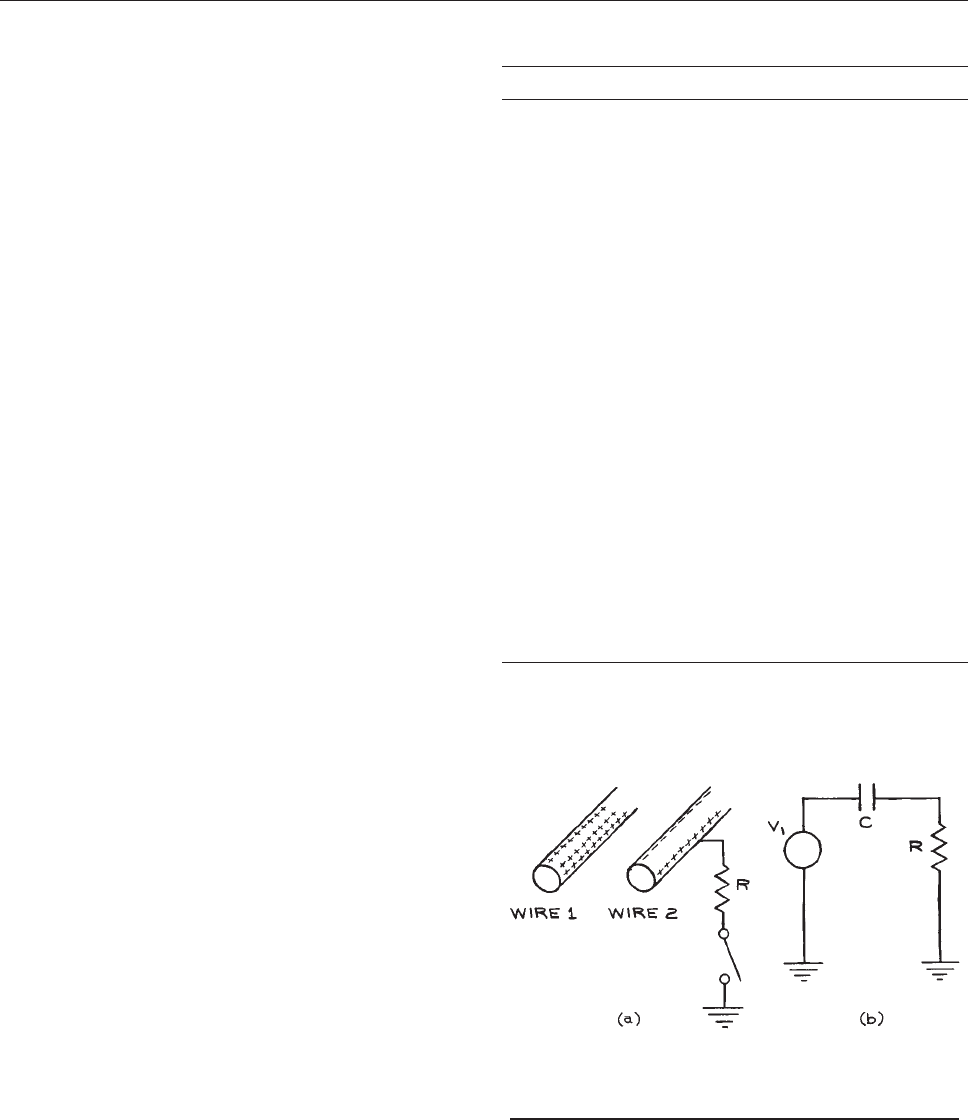
d.c. plus peak a.c. secondary voltage exceeds the voltage
rating of the tr an sform er insul ation, electrical breakdown
can occur, d estroying the transformer and possibly the
rest of the circuit. Isolation transformers are commonly
used to solve this problem. These transformers have a 1:1
turns ratio and high-voltage insulation between the pri-
mary and secondary windings. T he primar y is connected
to the a.c. line, while the secondary is connect ed to the
primary of the input transformer of the instrument to be
floated. In this way, the floating voltage appears across
the isolation-transformer windings. The case and controls
are still at the floating potential, and precautions similar
to those in the former situation must be observed. When
specifying an isolation transformer, the power-handling
capacity in watts or k ilovolt-amperes (KVA) as well as
the maximum isolation voltage must be considered.
A substitute for an isolation transformer is two high-
voltage filament transformers of the same turns ratio, con-
nected back to back. Such transformers are often used in
oscilloscope power supplies. This will produce the neces-
sary 1:1 overall voltage ratiowith isolation. Often such trans-
formers are more readily available and less expensive than
high-voltage, high-power, single-isolation transformers.
When floating instruments that are not directly powered
from the a.c. line, the external power supply (whether it is a
battery or line-operated supply) must be floated, too. The
precautions that apply to the floating of line-operated instru-
ments apply here also. Table 6.42 summarizes the important
co
nsiderations involved when floating power supplies.
6.9.2 Electrical Pickup: Capacitive Effects
It is often necessary to detect and measure electrical signals
in the millivolt and even microvolt range. If the signals are
accompanied by noise that is generated by external sources,
the signals can be so degraded as to render the measure-
ment useless. The elimination of external noise sources –
or, if this is not possible, the elimination of their effects – is
an important element in the design and construction of
electronic measuring, control, and detection systems.
Consider a wire at a potential V
1
in the vicinity of a
second wire that is insulated from all conducting surfaces
[see Figure 6.133(a)]. Coulomb forces between the
cha
rges on the surfaces of the wires will cause p olari za-
tion of the free charges in wire 2. Because wire 2 is
Table 6.42 Floating power supplies
(A) Normal Operation
(1) Input-line cord connected to three-terminal a.c. outlet
(2) Chassis at ground potential
(3) or + output terminal to grounded center terminal for a
+or output voltage
(B) Low-voltage floating operation
(1) Input-line cord to three-terminal a.c. outlet
(2) Chassis at ground potential
(3) + or terminal to floating potential
(4) Grounded output terminal unconnected
(C) Medium-voltage floating operation
(1) Input-line cord attached to 3-2 plug adaptor with ground
terminal unconnected
(2) Chassis at floating potential
(3) + or – output terminal connected to chassis output
terminal (at floating potential)
(4) Case and chassis isolated from all conductors
(5) Insulating shafts and knobs on all switches and dials
(D) High-voltage floating operation
(1) a.c. input from isolation transformer
(2) Instrument case at floating potential
(3) Case and chassis electrically isolated from all conducting
surfaces
(4) Insulated shafts and knobs on all switches and controls
Figure 6.133 (a) Capacitive coupling between two wires;
(b) the equivalent electrical circuit with the effect of wire 1
on wire 2 represented by C.
GROUNDS AND GROUNDING 503
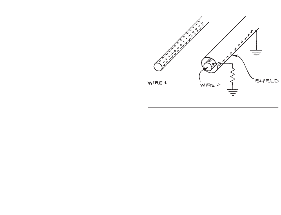
electrically isolated, it will remain e lectrically neutral. If
wire 2 is n ow connecte d to ground throug h a resistance R,
a current will momentarily flow due to the presence of the
positive charges on wire attracting negative charge to
wire 2 from the ground . The equivalent circuit is shown
in Figure 6.133(b). Typical values of the coupling capaci-
tance
are 1 to 100 pF. Two twisted #22 polyethylene-
insulated wires, for example, will have a c apacitance of
20 pF/ft. The center-wire-to-shield capacitance of RG/58
coaxial cable is 33 pF/ft. If we assume that V
1
is varying
sinusoidally at frequency x, the rms potential across R
is given by:
v
1rms
R
R þ 1=xC
¼ v
1rms
xRC
1 þ xRC
ð6:90Þ
(the voltage-divider formula). Thus the rms potential
across R increases with R, x, and C.
In the average laboratory, there are many sources of a.c.
voltage that can couple capacitatively to signal lines –
open-line sockets, lighting fixtures, and line cords are a
few examples. An estimate of the capacitance C
min
neces-
sary to induce a 1 mV rms voltage across 1 MX from a
power-line source can easily be made by setting V
1rms
equal to 120 V, x ¼ 2pf ¼ 188 rad/s, and neglecting
xRC with respect to 1:
C
min
¼
1 3 10
3
V
1:2 3 10
2
V 3 1:88 3 10
2
s
1
3 10
6
X
¼ 0:044 pF
ð6:91Þ
a value easily attained. Such induced voltages can be sub-
stantially reduced by the use of shielding. If a grounded
shield is placed around wire 2, the situation illustrated in
Figure 6.134 will occur. The conducting shield around
wire
2 will have a current induced in it when connected
to ground, due to the potential on wire 1. This current,
however, flows through a low-resistance connection. In
addition, and most important, any charge on the shield will
reside on the surface, and the interior will be field-free.
In practice, common coaxial braided shield is about 90%
effective against capacitatively coupled voltages from
external sources. Foil shields are even more effective.
6.9.3 Electrical Pickup: Inductive Effects
A c hanging magnetic field can induce a current in any
loop it cuts. The magnitude of th e induced current
depends on the area of t he loop and the time rate of
change of the magnetic field. High-resistance circuits
are not greatly affected by such inductive effects, but
they are important in low-resistance circuits, such as the
input circuits of curren t and pu lse amplifiers. Co mmon
sources of magnetic-field pickup are transformers,
inductors, and wires carrying large a.c. currents. Effec-
tive shielding against low-frequency magnetic fields is
accomplished with ferromagnetic enclosures that con-
centrate the stray magnetic fields within the shield
material. The usual practice is to enclose the source
of the magnetic fields within such shields. Higher-fre-
quency magnetic fields are best shielded with copper
enclosures. Ed dy currents induced in the copper pro-
duce counter magnetic fields. A rapidly changing cur-
rent is a source of time-varying magnetic fields that can
themselves induce currents in other circuits. Fast rise
time pulses in the low-impedance output circuits of
pulse amplifiers can generate rapidly changing mag-
netic fields that can in turn induce u nwanted currents
in nearby low-impedance input circuits. Once again, the
most effective shielding is h igh conductivity copper
sheet or foil.
Figure 6.134 Shielding to prevent capacitive coupling.
504 ELECTRONICS
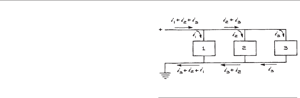
6.9.4 Electromagnetic Interference and r.f.i.
The high-frequency fluctuation of current or charge in a
conductor results in the radiation of part o f the energy in
the conductor in the form of an electromagnet ic wave.
Such a wave propagates through space at the speed of
light and, when not carrying useful information, is called
radio-frequency interference (r.f.i.). Sources of such
radiation are automobile ignition systems, microwave
ovens, electrical discharges, electric motors, electrome-
chanical switches and relays , and electronic switches
such as thyratrons, rectifiers, SCRs, and triacs. Power sup-
plies with switching regulators are often sources of r.f.i.
This interference can be reduced by the use of zero-
crossing switching regulators in which the switching only
occurs when the voltage across the switch is zero. The
most effective shield against r.f.i. is a grounded enclosure
of a conducting material, such as copper or aluminum. On
the surfaces of such a shield, the electric component of any
incident electromagnetic wave is zero and further propa-
gation is not possible. Conducting screens, rather than
solid sheet, are often used for r.f.i. shielding because of
the savings in weight. When using such a screen, it is impor-
tant that the mesh size be small compared to the wave-
length of the highest-frequency component of the r.f.i.
Standards have now been established for r.f.i. emission
from certain classes of electrical and electronic equipment.
Sensitive, high-frequency-measuring equipment must have
good immunity to r.f.i. and additional r.f.i. shielding can be
often purchased as an option for equipment that must oper-
ate in especially noisy environments.
6.9.5 Power-Line-Coupled Noise
Consider the case illustrated in Figure 6.135,wherea
single supply line powers three circuits. If circuit 1 sud-
denly requires a large amount of current, circuits 2 and 3
may be affected because of the resistance and inductance
of the power-supply line. A large current drawn by circuit
1 can caus e a momentary voltage dr op at circuits 2 a nd 3
that can be propa ga ted as noi se t hroughout t he circuit.
The greater the time rate of change o f the current pulse
through circuit 1, the larger the effect on the other
circuits. This probl em is very common with logic circuit s,
particularly TTL circuits, that h ave saturating out put
stages. If a number of gates switch simultaneously, very
large transient current spikes can appear on the power
line. These transients are then interpreted as a change in
logic level by other gates, and transitions occur that are
entirely spurious. Standard practice is to use low-resist-
ance, low-inductance power-supply lines to the logic
gates and decouple the gates f rom the power supply with
high-frequency capacitors from the power-supply termi-
nal of the gate to ground. For TTL, ever y group of 20
gates must be decoupled from the power supply with a 0.1
lF capacitor, and every group of 100 gates must be
decoupled wit h an a dditional 0.1 lF tantal um capacitor
with good high-frequency characteristics.
Similar situations arise with switched, high-current
devices such as temperature-controlled furnaces operated
directly from the a.c. line. Large current transients may
affect all equipment plugged into the same line. The only
remedy here is to operate the high-current device from a
completely separate line circuit.
As an example, consider a series of logic gates to be
connected to a power supply by 1 ft. of #22 wire, which has
a resistance of 16 X/1000 ft. and an inductance of 640 lH/
1000 ft. If a few gates switch simultaneously, resulting in a
current spike of 10 mA with a rise time t
r
of 10 ns, the
momentary voltage drop along the line will be approxi-
mately iZ, where Z is
ffiffiffiffiffiffiffiffiffiffiffiffiffiffiffiffiffiffiffiffiffi
R
2
þ x
2
L
2
p
. In this case:
Z ¼
ffiffiffiffiffiffiffiffiffiffiffiffiffiffiffiffiffiffiffiffiffiffiffiffiffiffiffiffiffiffiffiffiffiffiffiffiffiffiffiffiffiffiffiffiffiffiffiffiffiffiffiffiffiffiffiffiffiffiffiffiffiffiffiffiffiffiffiffiffiffiffiffiffiffiffiffiffiffiffiffiffiffiffiffiffiffiffiffiffiffiffiffiffiffiffiffiffiffiffiffiffiffiffiffiffi
16 3 10
3
XðÞ
2
þ 2p 3 3:3 3 10
7
s
1
3 6:4 3 10
7
HðÞ
2
q
ð6:92Þ
Figure 6.135 Current flow in three circuits on a common
power line.
GROUNDS AND GROUNDING 505
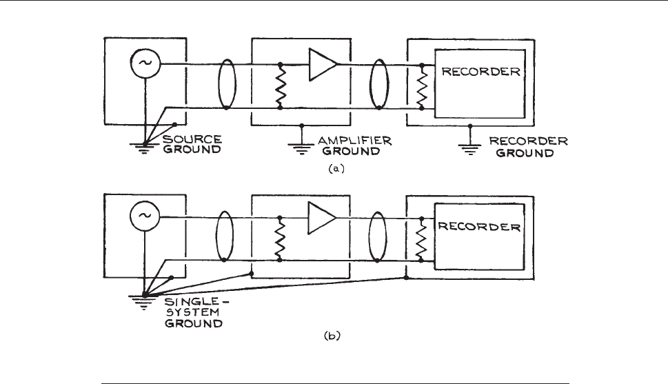
where x ¼ (2p/3)t
r
has been used in the estimate of the
inductive reactance of the wire. The voltage drop is then:
10
3
A 3 133 X ¼ 1:3V ð6:93Þ
For the TTL logic, this drop could be enough to cause
some marginally substandard gates to change state
momentarily.
6.9.6 Ground Loops
Instrument terminals are connected to ground in order to
have the potentials of those terminals be at 0 V for refer-
ence purposes, assuming that every ground connection is
made directly to the zero potential of the earth. This is
often not the case, since most ground connections are
through the third wire of the a.c. line. Since this line has
finite resistance, currents flowing in it will cause potential
drops and, depending on the point on the line where a
ground connection is made, the potential can be substan-
tially different from 0 V. When the 0 V references of two
instruments that are connected together differ, there is
danger of introducing noise into the system. The problem
is made all the worse by the fact that the reference points
can change their potentials with respect to each other in a
way independent of other system parameters. The solution
to this problem is to have only a single ground point in the
system and connect all the zero reference points and
shields to it. This means removing the ground connections
in the power-line cords of all line-operated instruments,
and isolating all shields and cases from conducting surfa-
ces that may be connected to ground at points other than
the single system ground. All connections to this single
system ground should be made as short as possible, with
the lowest-resistance conductors available. By having the
0 V reference potential connection and shield connection
at the same point in the system, no currents can be induced
in the reference line.
To illustrate these ideas, two different ways of connect-
ing a system composed of a signal source, amplifier, and
recorder are shown in Figure 6.136. In the top arrangement
each
case is separately grounded and also connected to the
other cases through the outer conductor of the coaxial
cable between them. If the three grounds are at different
Figure 6.136 System grounding: (a) multiple grounds; (b) single ground to eliminate
ground loops.
506 ELECTRONICS
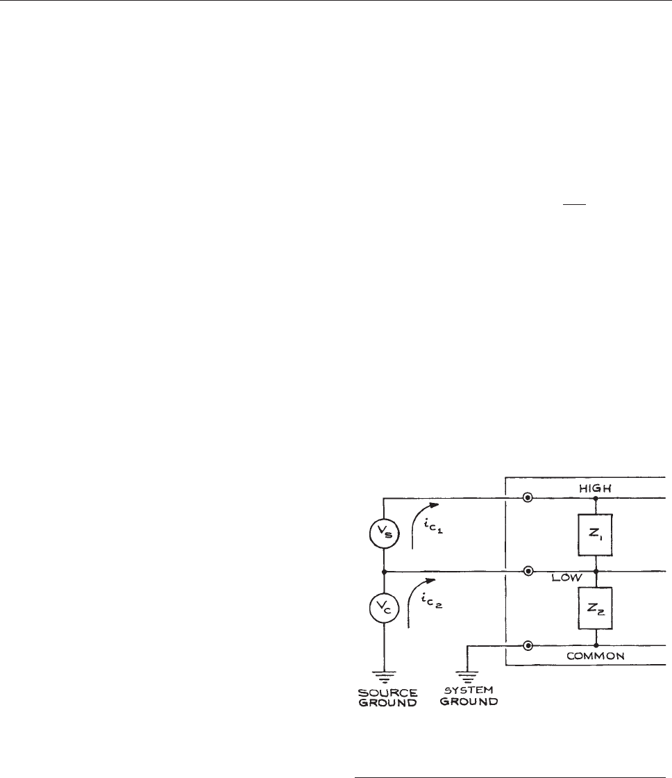
potentials, currents will flow through the coaxial outer
shields connecting the devices together. Since the refer-
ence-potential line is the shield, it will take on different
potentials at different points in the circuit. As these poten-
tials change, the signal levels will change – the result being
seen as noise on the signal line.
In the second ar rangement , the common reference line
and the instrument shields are all attached to ground at a
single point – the reference ground. No gro und l oo ps c an
exist, and the reference line remains at the same potential
everywhere in the system. Clearly this is a su perior
arrangement. The imple mentation may be difficult, how-
ever, since it is necess ary to connect all the cases and
shields separately to a single ground point. If all the
instrumentsaremountedinasinglerack,eachmustbe
electrically isolated from the conducting rack structure.
The coaxial-shield connections must al so be isolated
from the cases, an d the ground conn ectio n in the a. c. l ine
cord must be removed from each of the instruments. It is
not always necess ary to t ake such precautions with all
stages o f a system – it may be sufficient to eliminate
ground loops from the most sensitive element to which
the signal source is connected.
It is worthwhile to understand the origins of ground
loop and shielding problems in order to be able to s ol ve
them when they arise. An ext ensive treatment is given by
Morrison.
14
The problem of ground loops also occurs when meas-
urements must be made across two electrical terminals,
neither of which is at ground potential.
15
Bridge measure-
ments are a common example of this. For floating meas-
urements, instruments that have the reference input
terminal electrically separate from the ground or common
terminal must be used, otherwise the floating potential
(common-mode potential) will be short-circuited.
In Figure 6.137, v
S
is the source voltage to be measured,
v
C
is the common-mode voltage, Z
1
is the input impedance
of the measuring system, and Z
2
is the impedance from the
common of the measuring circuit to the low terminal –
normally 10
8
to 10
10
X in parallel with 10
3
to 10
5
pF. The
presence of v
C
results in currents i
C1
,andi
C2
flowing
through Z
1
and Z
2
. This presents no difficulties so long as
the resistance of the lines is zero; if the resistances are finite,
the common-mode currents will result in potential differ-
ences at the low input terminal and add to the error of the
measurement. Generally, Z
1
<< Z
2
and the critical parameter
is the ratio of the resistance of the low signal line to Z
2
. This
ratio is frequency-dependent, because Z
2
is complex. If the
source and instrument grounds are not at the same potential,
the difference will add to v
C
.
The common-mode rejection ratio (CMRR) is a quan-
tity for specifying how well an instrument rejects a com-
mon-mode voltage superimposed on the voltage to be
measured (the normal mode voltage):
CMRRðdBÞ¼20 log
v
NM
v
CM
, ð6:94Þ
where v
NM
is the portion of the common-mode voltage that
appears as a normal-mode voltage, and therefore a source of
error. Meters that can be floated have CMRRs from 80 to
120 dB at d.c. and 60 to 100 dB at line frequency. When
higher values are required, special voltmeters having an
additional guard terminal must be used. This terminal,
when connected to the low terminal of the source by a low-
resistance connection, shunts the common-mode current
from the measuring terminals. Such meters offer CMRR
values of 160 dB at d.c. and 140 dB at line frequency. For
a meter with a CMRR of 160 dB, a 10 V common-mode
signal will result in a 0.1 lV normal-mode voltage.
Figure 6.137 Measurement of v
s
across two terminals,
both of which are not at ground. Current flow through Z
2
,
the impedance from the low terminal of the measuring
instrument to ground, will result in an error voltage.
GROUNDS AND GROUNDING 507

6.10 HARDWARE AND
CONSTRUCTION
It is almost always better to purchase a piece of electronic
equipment than to design and construct it. This is certainly
the case for power supplies, amplifiers, signal generators,
and similar equipment that is mass-produced by a large
number of companies in a wide variety of models.
When one does, however, decide to construct a piece of
electronic equipment because of cost or the unavailability
of commercial units, there are a number of well-defined
steps to follow:
(1) Design of the circuit
(2) Selection of components
(3) Construction and testing of a breadboard model
(4) Construction of the final circuit
(5) Mounting
(6) Final testing.
Except for the simplest circuits, one is well advised to
use proven designs that can be found in manufacturers’
application books and in books and articles on circuit
design. A few such publications are given in the list of
references.
16
There are, in addition, well-established tech-
niques that are used by electronic engineers (but not often
included in textbook examples of circuit design) that can
make the difference between a circuit that works and one
that does not. These include bandwidth limiting, power-
supply decoupling, and signal conditioning.
6.10.1 Circuit Diagrams
Two kinds of circuit diagrams are the block diagram and
the schematic wiring diagram. The block diagram shows
the logical layout of the circuit by grouping all elements
necessary for a single function into a single rectangle.
Although simple, such diagrams are very useful in under-
standing the general operation of a circuit. The block dia-
gram is much like the flowchart of a computer program.
The schematic wiring diagram shows all the compo-
nents of the circuit and the connections between them.
Figure 6.138 lists symbols used in schematic diagrams.
The
more complete the schematic, the more useful it is
for troubleshooting. A schematic will have the values
and ratings of all the components, as well as numbers
and color codes when necessary. Good schematics include
the values of voltages at critical points in the circuit and
drawings of waveforms where appropriate. One generally
reads schematic diagrams starting at the upper left with the
input and proceeding to the lower right to the output.
A useful addition to the schematic diagram is the chassis
layout diagram, which shows the physical location of all
parts. For ease of drawing, components that appear next to
each other on the schematic may be far away from each
other on the actual chassis or circuit board.
W ith increasing use of integrated circuits, it is more and
more difficult to identify the functions of dif ferent elements
in a schematic. This is because the integrated circuits are
often only represented by rectangles with pin numbers. To
identify their function, it is necessary to consult a manufac-
turer’s catalog. Abbre viations common with ICs are gi v en in
Table 6.43 along with representati ve package outlines. Sche-
matic
diagrams also help identify specific components. If
there is an operational amplifier on a circuit board with a
balance control near it for nulling purposes, it is useful to
know where the amplifier is in the circuit and the nature of
the input and output before proceeding with adjustments.
The location of damaged components can be useful infor-
mation when deciding on the probable cause of the damage
and other components that may also have been af fected.
6.10.2 Component Selection and
Construction Techniques
When selecting components, the considerations that an elec-
tronic engineer finds important may be dif ferent from those
of a laboratory scientist building only a single example of a
circuit. It is always wise to overspecify components – that is,
to use components of higher ratings and better quality than
a critical cost-effective analysis of the circuit would show
to be necessary. Usually the cost of components is a small
fraction of total project cost when time is considered.
Once the circuit design has been decided upon and the
components assembled, a breadboard model can be con-
structed. This may seem an unnecessary and time-
consuming step, but care at this stage will save a great deal
508 ELECTRONICS
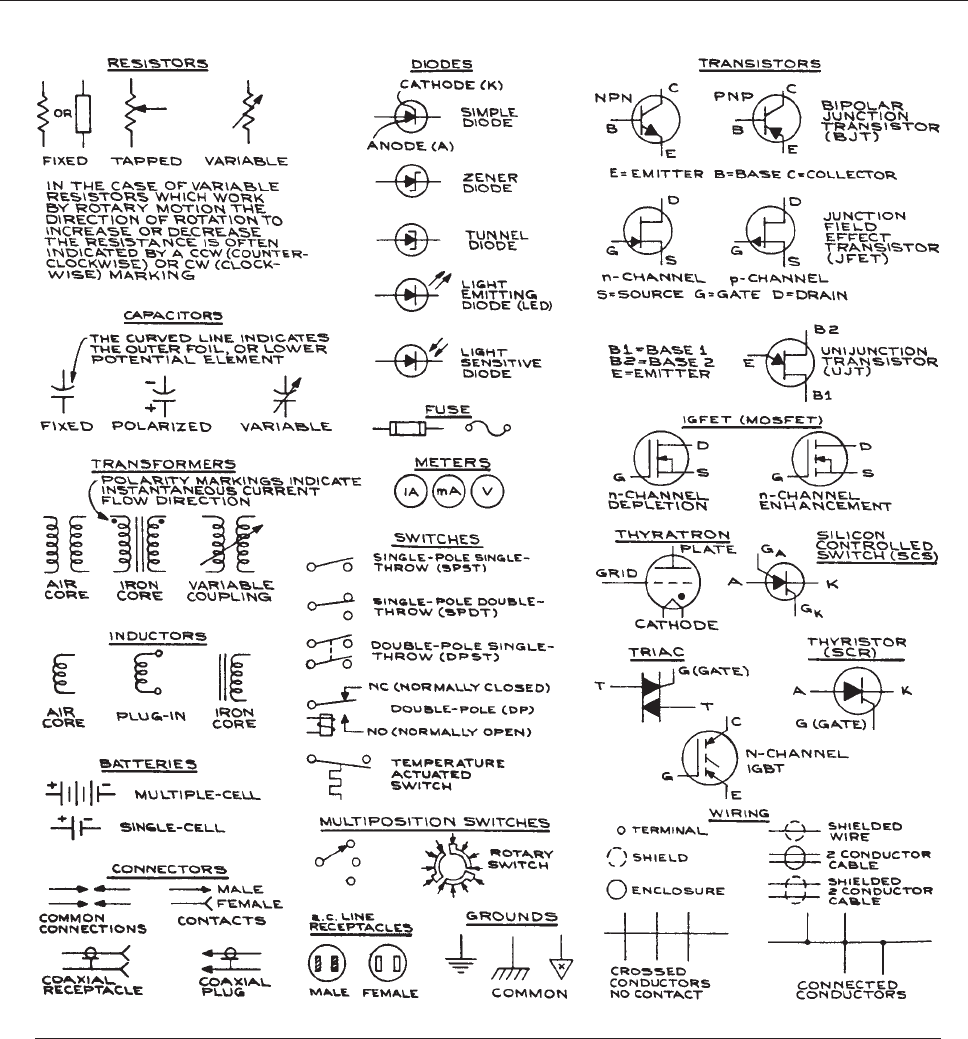
Figure 6.138 Symbols for schematic circuit diagrams.
HARDWARE AND CONSTRUCTION 509
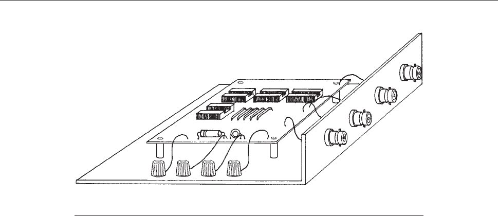
of time later. The breadboard circuit should be constructed
from a complete, detailed schematic circuit diagram.
There are a number of prototype circuit boards and aids
for making breadboard models. Prototype boards use sock-
ets to which components and wires can be connected in a
temporary way . The spacing of the sockets is usually on .1 in.
centers to accommodate the usual 14- and 16-pin dual
in-line integrated circuits. The sockets accommodate only
a limited range of solid-wire sizes. Outside of this range, the
wire is either not held securely or the socket is bent out of
shape. Prototype boards of thi s type are satisfactory for low-
frequency circuits and logic circuits using TTL and CMOS.
For sensitive high-frequenc y circuits and ECL logic, stray
capacitance between sockets is a problem, and such circuits
must be built on a circuit board with a ground plane if they
are to work properly.
17
At this stage it is necessary that the
breadboard circuit follo w the schematic in ev ery detail. The
mechanical layout should be neat, with interconnections
between components as short as possible. This simplifies
troubleshooting and avoids pickup problems.
Interfaces to external power, and input and output cir-
cuits, present some difficulty when working with bread-
boards. Dangling wires and alligator-clip connections
invite short or open circuits and damaged components.
Whenever possible, the breadboard should be mounted on
a larger structure with terminals and connectors to which
semi-permanent power-supply and signal connections can
be made (see Figure 6.139). Connections from these termi-
na
ls to the breadboard can then be made with short lengths
of hookup wire.
The breadboard circuit should be fully tested before
proceeding to the final construction stage. During testing
the circuit should be operated with the same input and
output connections the final circuit will have.
Once the breadboard circuit is functioning properly, the
final circuit can be constructed. Depending on the complex-
ity of the circuit, there are a number of construction techni-
ques available. In general, all components are mounted on
circuit boards with the boards fitted into a case or attached to
a panel. The power supply can be incorporated into the
circuit, or power-supply voltages can be brought in from
the outside-through connectors. For simple low-frequency
circuits involving only a few components and a moderate
number of connections, perforated circuit board and push-in
terminals can be used [see Figure 6.140(a)]. To avoid bend-
ing
the terminals when they are inserted in the board, an
insertion tool matched to the terminal should be used. All
connections are individually made and soldered for such
circuits. Whenev er possible, activ e components such as
ICs and transistors should be used with sockets, and all
soldering done with the components removed from the sock-
ets. Perforated circuit board with printed circuit wiring is
also a conv enient medium for making final circuits [see
Figure 6.140(b)]. With this type of circuit board, all solder-
ing
is done on the board and there is no need for separate
terminals. To facilitate bringing power to the components,
Figure 6.139 Circuit breadboard mounted to chassis on standoffs to allow proper con-
nection of power supply, input and output leads.
510 ELECTRONICS
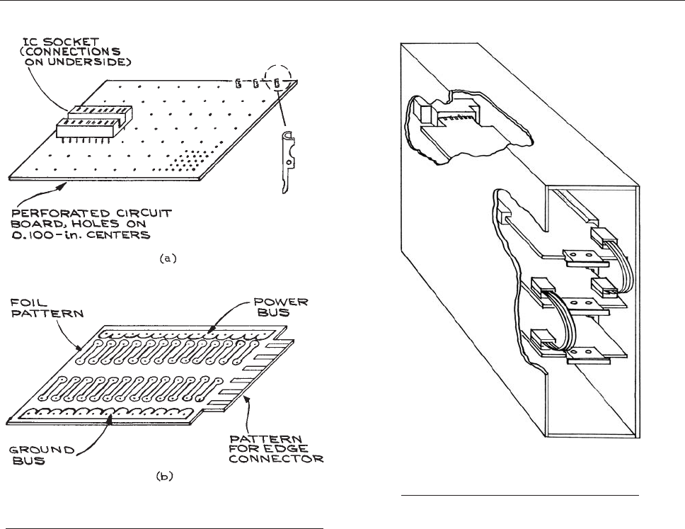
power-supply and ground-bu s structures are often part of
such boards. For more complex circuits, custom-printed cir-
cuit boards (see Section 6.10.3)orWireWrap
TM
boards (see
Section 6.10.4) can be used.
The
circuit board containing all the electrical compo-
nents and a power supply, if required, is typically mounted
on a standard 19 in. aluminum rack panel on standoffs.
When there is a need for more than two or three circuit
boards, the means of mounting and of making the inter-
connections must be considered more carefully. For multi-
ple circuit boards, card-cage mounting – using guides and
edge connectors, as shown in Figure 6.141, is a common
technique.
Interconnections between boards are made
between the edge connectors on the rear panel of the chas-
sis. A variation of this method uses a motherboard, to
which all the connections from the other boards are
brought. In this method, the edge connectors provide
power to the separate boards and help to mechanically
retain the boards in the chassis. Signal leads are brought
to the motherboard via multiple-pin connectors and flat
multiple-conductor cable, using mass termination hard-
ware for increased reliability. A variation of the mother-
board configuration includes the edge connectors on the
motherboard. An on–off switch, pilot light, and fuse are
put on the front panel, as well as input and output con-
nectors and controls. When labeling the panel, it is wise
to indicate schematically the electronic functions per-
formed by each section of the circuit with standard
symbols. Labels can be applied with the silk-screen
Figure 6.140 Perforated circuit boards for use with (a) pin
connections and (b) direct solder connections.
Figure 6.141 Circuit boards mounted in a
card cage showing interconnections and
guide slots.
HARDWARE AND CONSTRUCTION 511
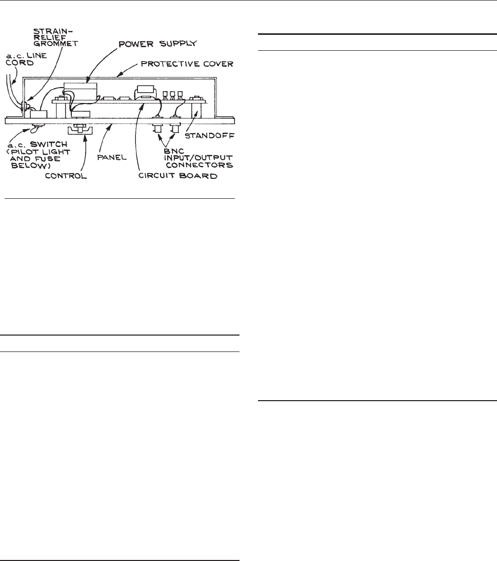
technique or dry transfer letters, India ink, or embossed
pressure-sensitive tape. A protective cover should be
placed over the circuit (see Figure 6.142).
Construction
can be simple. A portable electric drill
or drill press is necessary for drilling proper-sized holes
in panels and covers. A list o f electronic-circuit c on-
struction tools is given in Table 6.43 and a list of useful
ha
rdware is given in Table 6.44. Flathead screws should
b
e used on exterior surfaces, and lock washers should be
used under nuts. Standard .062 in. circuit board can be
cut easily with a hacksaw and drilled with standard high-
speed drills. A nibbling tool is u seful for making irreg-
ular-shaped holes in sheet metal, and a set of chassis
punches fro m 1/2 to 1 1/2 in. speeds up work and makes
accurate holes in sheet metal. A tapered hand reamer is
very useful for enlarging holes in sh eet metal and circuit-
board material.
Figure 6.142 Mounting of a circuit board on a rack panel.
Table 6.43 Electronic-circuit construction tools
Nutdrivers
Sheet-metal nibblers
Universal electrician’s tool
Needle-nose pliers
Slip-joint pliers
½-in tapered reamer
Wire cutters
Wire strippers
Soldering gun, pencil
Knife
Single-edge razor blades
Solder sucker
Solder wick
Heat gun
Clip-on heat sinks
Chassis punches
5=8,3=4,1ð1=8Þ,1ð1=4Þin:Þð
Circuit-board holder
Note: These tools supplement those listed in Table 1.1.
Table 6.44 Hardware and electronic equipment
Hardware
Screws (flathead and roundhead), nuts, flat washers, lock
washers (4–40, 6–32, 10–24)
Solder lugs and terminals
Binding posts
Grommets
Standoffs
Cable clamps
Line cord
Hookup wire
Spaghetti (flexible thin insulating tubing) in assorted sizes
Shrink tubing in assorted sizes
Eyelets
Fuse holders
Indicator lamps
Switches
Electronic Equipment
Signal sources:
Signal generator
Pulse generator
Logic pulse source
VOM/DVM
Oscilloscope
Logic probe
Logic clips
Test leads for VOM and DVM
Oscilloscope probes:
3 1 probe for low frequencies
3 10 compensated probe for frequencies above 10 MHz
Radio-frequency probe for demodulating r.f. signals
512 ELECTRONICS

6.10.3 Printed Circuit Boards
The use of PCBs in laboratory electronics is justifi ed when
sev eral identical boards are needed or when the proper func-
tioning of the circuit requires the kind of controlled geome-
try that printed circuit boards offer. Emitter-coupled logic
(ECL) circuits require microstrip line geometries for inter-
connections and precise placement of components to achiev e
fast rise times while at the same time avoiding crosstalk
between circuit elements. Sensitiv e lo w-l e v el amplifier cir-
cuits require precise lead placement to eliminate noise
pickup. Printed circuit boards consist of an insulated sub-
strate covered with a metal (usually copper) foil. Some of the
common rigid substrates used for copper -clad boards are
listed in Table 6.45 along with their codes. Nonrigid boards
or fle
x-boards are used to fit into irregular confined spaces.
Commercial production of PCBs begins with copper-
clad laminated boards, usually epoxy-impregnated fiber-
glass .062 in. thick, from which copper is removed by
chemical etching to form the pattern of traces, pads, and
busses that are the electrical connections and mounting
areas for the individual electronic components and connec-
tors. To increase circuit density, patterns can be formed on
both sides of the board with electrical connections between
the layers made by plated holes or vias. Sandwiches of up
to four boards (eight layers) are common, and current man-
ufacturing capabilities permit as many as 40 layers. After
fabrication of the board pattern, holes are drilled for com-
ponent leads, vias, and fasteners – a thin layer of solder
(solder plate) is flowed over the copper and through the vias
to protect from oxidation and increase the ease of compo-
nent soldering. Solder mask – a thin, tough, insulating film
– is placed over the board, leaving only the solder terminals
and pads uncovered. The mask protects the traces, acts as
an insulator to prevent short circuits, and prevents solder
bridges from occurring when components are soldered to
the board. Component outlines and descriptive information
are printed on the board using a silk-screen technique.
The circuit patterns are photographically transferred
to the boards using photo-plots and photo-resists. The
photo-plots are the equivalent of a photographic negative
and contain all of the detail at the required precision of the
final circuit board. In the past, photo-plots were made by
hand with opaque tape and precut pads and pad arrays, but
this has been commercially superseded by CAD/CAM
(computer aided design/computer aided manufacture)
programs that are now widely available for PCs. These
programs have two parts – schematic capture and board
layout. Simulation software is often available within the
layout programs to verify the functioning of the circuits for
a variety of input signals. Printed circuit boards produced
with CAD/CAM software have a number of advantages,
even at the single board prototype level:
Uniform electrical and mechanical properties as a result of
using standard materials and automated fabrication meth-
ods based on standard electronic and mechanical engineer-
ing con v entions that are built into the CAD/CAM programs
Error checking in the schematic-capture routines
Linking the output of the schematic-capture program to
circuit-analysis programs for evaluation of the circuit
Table 6.45 Circuit-board subtrates
Type of board material Designation Application
Paper-base phenolic XXXP Hot punching
XXXPC Room-temperature punching
Paper-base phenolic FR-2 Flame-resistant
Paper-base epoxy resin FR-3 Flame-resistant
Glass-fabric-base epoxy resin FR-4 General-purpose flame-resistant
FR-5 Temperature and flame-resistant
G-10 General purpose
G-11 Temperature-resistant
Glass-fabric-base polytetrafluoroethylene resin GT and GX Controlled dielectric constant
Note: Standard thicknesses, including the copper clad ding, range from 1/32 (0.031) to 1/4 (0.250) in., with 1/16 (0.062) in. the most common.
HARDWARE AND CONSTRUCTION 513

Electronic recording and transmission of the photo-plot
(Gerber), drill, solder mask, silk-screen, and outline files
Competitive pricing and fast turnaround.
These advantages have to be weighed against the incon-
venience of modifying printed circuit boards that are only
meant to be prototypes, and having to acquire and learn the
CAD/CAM software. Manufacturers of schematic-capture
and PCB-layout programs are listed at the end of this chap-
ter. Trial versions of their software products are generally
available and many offer student and educational institution
discounts. A number of PCB fabricators make available
layout programs that are easy to use for relatively simple
circuits. Procedures for producing commercial PCBs using
schematic-capture and board-layout programs are detailed
in the following two sections.
Schematic Capture. A schematic diagram of the cir-
cuit is laid out on the computer using components from the
program library. Components not in the library can
sometimes be obtained from the manufacturer of the com-
ponent. The library entry contains mechanical and electrical
information about the component, as well as the numbering
and designation of the pins and/or terminals. Layout is
accomplished by arranging the components on the com-
puter screen with the mouse or by specifying coordinates
and then interconnecting the pins of the components. Each
connection is a node. From the schematic arrangement, a
netlist is made. This is a list of all the components along
with their electrical parameters and the nodes to which they
are connected. The netlist is the basis of various error-
checking routines to verify that inputs and outputs are not
grounded and that no component is shorted.
Board Layout. The netlist from the schematic-capture
program is the input to the board-layout program. Layout
starts by defining the size and shape of the board and the
number and designation of layers. For a two-sided board,
one side (the top) is the component side and the other (the
bottom) is the wiring side – even though there will gener-
ally be wiring on both sides.
Componentsareplacedontheboardfromastackofout-
line drawings (rat nest) with connections specified by the
netlist. The components with their accompanying wires are
initially arranged within the board area according to a few
simple rules: separate input and outputs by as large a distance
as possible; make po wer-supply and ground connections as
short as possible; minimize the number of crossed traces; and
horizontal and vertical routing of traces. Final routing of the
connections is done manually for small, uncomplicated
boards with only a few components. Autorouting routines
are useful for complex boards, but hand routing may still
be necessary in certain circumstances. For small boards, it
is possible to skip the schematic-capture part of the procedure
and go directly to the board-layout routine. In this case, parts
are placed manually and interconnections made individ ually.
When parts are available in the program library, this can be
an efficient method for board layout, but all automatic error
checking is lost with manual parts placement. Table 6.47 lists
impo
rtant PCB layout considerations.
The PCB manufacturer requires computer files to fabri-
cate the boards. These files are routinely transferred elec-
tronically over the Internet. The files specify the board
layout, board size and shape, hole pattern, solder-
Table 6.46 PCB construction considerations
(1) Board size, shape material [ 1=16 in: G10 is most common
with 1 oz./ft.
2
(35 lm) copper cladding]
(2) External connections
(a) Solder or wrapped to terminals
(b) Plugs
(c) Edge connectors
(3) Mounting
(a) Screws
(b) Guide slots and edge connector
(4) Component layout
(a) Mechanical stress
(b) Thermal stress
(c) Inputs and outputs separated to avoid positive feedback
(5) Lead layout
(a) 1=16 or 0.050 in. preferred width; no sharp corners
(b) 0.015 in. minimum lead clearance, larger in the vicinity
of solder connections
(c) Crossovers
(i) Insulated wire bridges for few crossovers
(ii) Double-sided board and plated-through holes for
many crossovers
514 ELECTRONICS
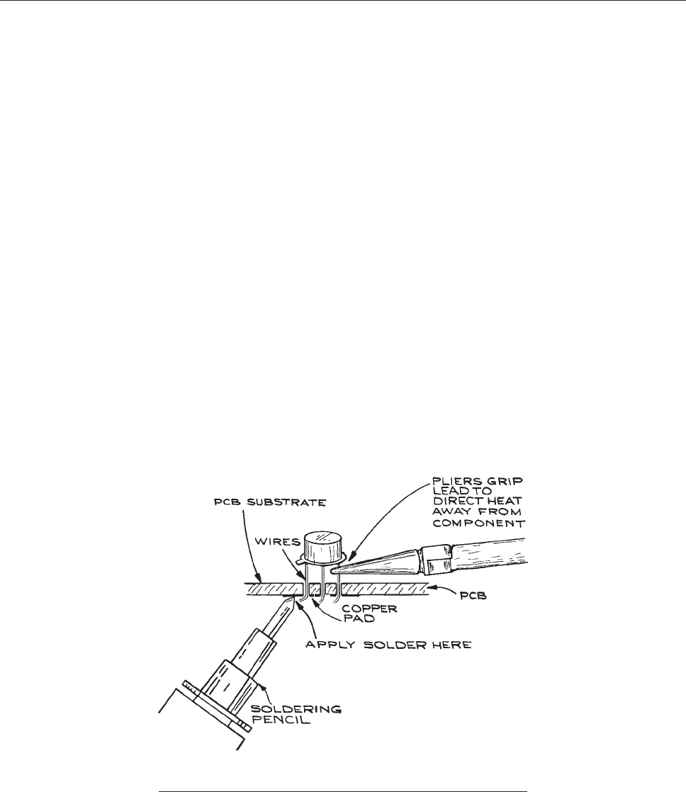
mask pattern, and silk-screen labels and outlines. It is essen-
tial that the files follow precisely the format required by the
manufacturer. There is one Gerber file and one aperture file
per layer. The Gerber file specifies the interconnections and
the aperture file gives the widths of the traces. If solder mask
and silk-screen printing are used, each requires a Gerber file
and aperture file per layer . Holes are specifi ed by a drill file
and a drill list file. For laboratory purposes, the FR-4 grade
board is the current standard. The copper-foil cladding is
usually cathode-quality, electrolytic copper. The most com-
mon thickness is 1.0 oz./ft.
2
(35 lm). Turn-around time for
double-sided boards is generally three to fiv e days. A rectan-
gular , double-sided board, 3 in. by 5 in, costs less than $100.
Per board prices fall substantially for two or more boards.
Components are fixed to PCBs by soldering. For large,
complex, multilayer boards, the PCB manufacturer will
often have the capacity to automatically locate parts on
the board and solder them in place using wave soldering
for through-hole components and reflow methods for
surface-mount components. For surface-mount parts a sol-
der-paste mask is used. This mask has openings corre-
sponding to the solder pads. It is placed on the board,
properly aligned in relation to the pads, and solder paste
is squeezed over it. When the mask is removed, solder
paste covers only the pads, the components can then be
placed in position ready for soldering. When hand solder-
ing, through-hole wire lead components are held in place
on the board by inserting the leads through the appropriate
holes in the board and bending them outward at 45°. The
board can then be turned over for soldering the leads to the
pads. After soldering, the leads are clipped short with flush
cutting pliers, see Figure 6.143. Soldering surface mount
components
is more difficult and takes some practice.
When the pads on the board have a solder reflow finish,
soldering is easier than if solder has to be added. With
reflow finish pads, flux is first applied to the pads from a
flux pen or syringe and the component placed in position
with leads aligned with the pads. The component is then
tacked in position by heating opposite corner pins with a
fine-tip, well-tinned soldering iron from which all excess
solder has been removed. Each pin is then heated in
sequence to melt the solder and form a high conductivity
joint. It is wise to repeat this procedure a second time to
insure the secure soldering of all the pins. The board can be
examined under a strong light source to check for solder
bridges. Bridges can be removed with solder braid.
For boards without a solder plate finish, surface mount
components can be soldered in place using the same gen-
eral technique, but with a thin coating of solder on the iron
tip. As the tip is wiped over the component leads solder
Figure 6.143 Pliers used as a heat sink. A heat sink is required when
soldering to the leads of heat-sensitive components.
HARDWARE AND CONSTRUCTION 515
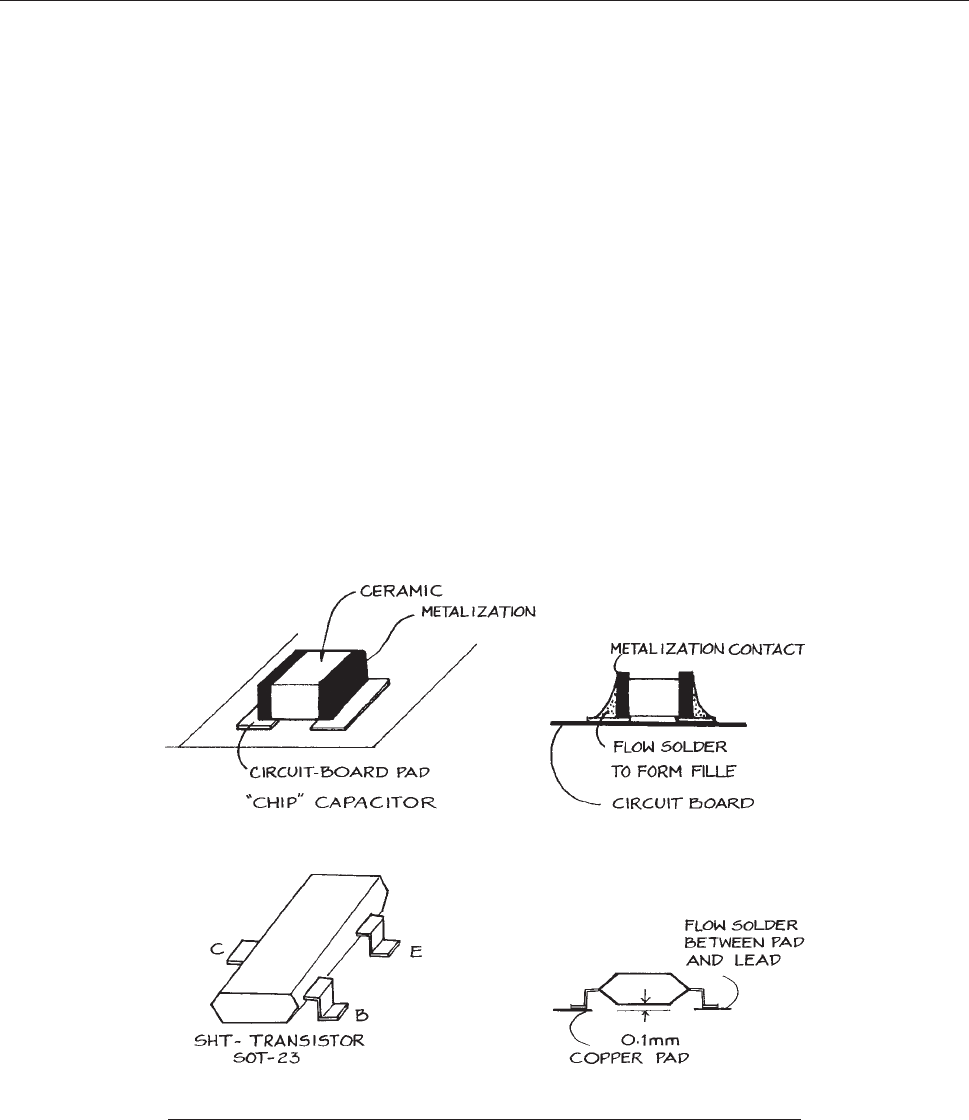
is transferred from the tip to the leads and pads making
effective solder joints. With this technique, solder bridges
are more likely and careful inspection is required.
To solder surface-mount resistors and capacitors, solder
must flow over the circuit-board pad and component
contact. This is illustrated in Figure 6.144. To solder sur-
f
ace-mount transistors and ICs with coarse-pitch leads to
circuit-board pads it is necessary that solder flow between
the component contacts and pads. Fine solder, and fine-tip-
ped soldering iron, a low-po wer binocular microscope, and
steady hands are required for these component s. Solder flux
dispensed from a pen or syringe with a fine tip can be applied
to the pads and the component contacts set down on top of
the flux. The contact is then heated with a fine-tip soldering
iron and fine wire solder applied until the solder melts and
wets the component contact and circuit-board pad.
Although commercial production of PCBs from master
artwork has been replaced by fabrication directly from com-
puter files, it is still possible to make a PCB from hand-drawn
artwork with kits that are available from electronics suppliers.
The kits consist of circuit boards and sensitizers or presensi-
tized boards, dev eloper, ferric chloride etchant, and trays and
brushes. The first step is creation of the artwork master , a
precise representation of the final traces that will appear on
the board. The master is produced using drafting techniques.
To increase speed and accuracy of manual drafting, PCB dry-
transfer drafting tapes, socket-hole patterns, and terminal
pads are av ailable. The tools needed are a T-square, triangles,
an X-ActoÔ knife to cut the tape to length, and tweezers for
removing the dry transfers from the backing sheet. To avoid
dimensional changes with temperature and humidity, the art-
workcanbepreparedonMylarÔ drafting film rather than
ordinary paper. The pattern on the master photographic neg-
ativ e is transferred to the circuit board by the use of a photo-
resist sensitizer. Boards can be purchased presensitized, or
unsensitized blanks can be coated with a photoresist that is in
aerosol or liquid form. A ne gative resist, after exposure to UV
light, is unaffected by a subsequent developer solution,
whereas UV-exposed, positive resist is dissolved by dev el-
oper. If the master artwork is a positive (that is, the desired
foil pattern is represented by opaque areas on a transparent
background), a positive resist is required. The sensitized
Figure 6.144 Soldering surface-mount (SMT) components.
516 ELECTRONICS

board is exposed to strong light through the full-size master .
The board is then placed in a glass tray containing de veloper.
Areas on the board exposed to the light will be dissolved,
while those areas protected by the artwork will remain.
After full development, the board is rinsed, dried, and placed
in an etching solution. It is also possible to laser print or
photocopy circuit designs directly onto specially coated trans-
fer paper – available from JDR Microdevices – that is then
ironed on to a blank PC board, which is then ready for etching.
Sev eral electronics suppliers sell resist pens that are used to
draw PCB artwork directly on bare circuit board. Ferric chlor-
ide is the most common etchant. It works best when gently
heated and agitated. Full etching can take up to one hour per
board and should always be done in a glass tray. When etching
is complete, the board is rinsed and all etchant residues
removed with steel wool or a solvent. A more complete
description of the procedure is giv en in the 1999 edition of
the ARRL Handbook for Radio Amateurs. The photoresists
have limited shelf life, and the etchant is corrosiv e.
Transistor and integrated circuit packages for PCB
mounting come in a wide variety of forms. Table 6.47 gives
the
designation of some common packages with represen-
tative diagrams.
A technique related to PCBs and based on thick-film tech-
nology is used to pr oduce high-density circuit patterns on
alumina (Al
2
O
3
) substrates. A screen with 200 to 300 lines/
in. transfers the desired circuit pattern with a special ink
containing suspended metal particles and a binder. When
the inked substrate is fired, the metal particles fuse to each
other and the substrate, producing a tightly bonded con-
ducting pattern. Components are then soldered to the
appropriate pads on the substrate with microsoldering irons
or solder paste and carefully controlled hot air. Thick-film,
rather than discrete, resistors are often used with this tech-
nique because they can be produced by the same printing
technique by using a different ink. Small, high-capacitance
chip capacitors replace the more conventional disc and
tubular capacitors. With the thick-film technique, it is often
quite easy to incorporate ICs and discrete components on
the same substrate to produce a self-contained hybrid cir-
cuit. Such a circuit can be hermetically sealed and has the
appearance of a large IC. The advantages of such circuits
are small size, excellent electrical properties, and good
mechanical strength. There are a number of companies that
produce hybrid circuits starting from schematic diagrams.
Because of its specialized nature, thick-film work is best
left to such firms.
Solder for electrical and electronic work is an alloy of tin
and lead and is specified by the ratio in weight % tin to lead.
Thus 40/60 solder is 40% tin and 60% lead by weight. An
Table 6.47 Transistor and integrated circuit packages
Transistor
TO-3 Round Can on Diamond Base
TO-5 Round Can
TO-220 Rectangle with Heat Sink
Through Hole IC
DIP Dual In-Line Package
PDIP Plastic Dual In-Line Package
SIL Single In-Line
SIM Single In-Line Module
SIP Single In-Line Package
VIL Vertical In-Line
ZIP Zig-Zag In-Line Package
Surface Mount IC
PSMC Plastic Surface Mount
Component
QSOP Quarter Size Small Outline
Package
SOIC Small Outline IC
SOL Small Outline Large
SOP Small Outline Package
SOT Small Outline Transistor
SSOP Small Shrink Outline Package
TQFP Thin Quad Flat-Pack
TSOP Thin Small Outline Package
TSSOP Thin Shrink Small Outline
Package
IC Modules
BGA Ball Grid Array
DIMM Dual In-Line Memory Module
JLCC J-Lead Chip Carrier
LCCC Leadless Ceramic Chip Carrier
LDCC Leaded Ceramic Chip Carrier
PGA Pin Grid Array
PLCC Plastic J-Lead Chip Carrier
SIMM Single In-Line Memory
Module
HARDWARE AND CONSTRUCTION 517
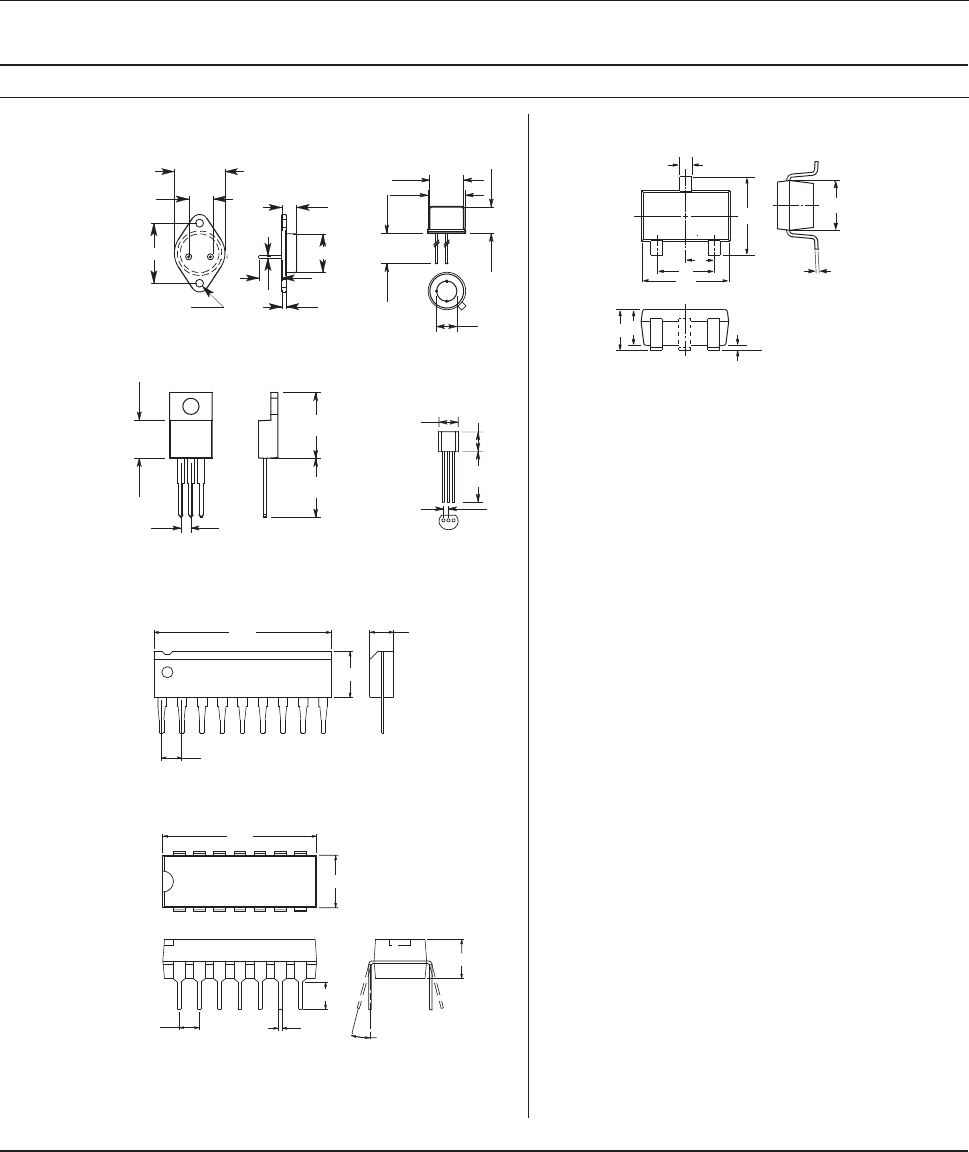
Table 6.47 (cont.). All dimensions in mm
C
L
C
L
C
L
12 3
456
C
L
SEATING
PLANE
.95
.90
.05
2.0
1.3
.65
2.10
.32
.14
1.25
3-Lead SOT, Small Outline Transistor
TO-3
9 Lead SIP
14 Lead PDIP
TO-220
TO-5
TO-29
E
B
C
6.6
5.1
3.8 MIN
8.5
9.4
4.8
4.8
12.8
1.3
Transistor
Through Hole IC
Surface Mount Transistor
9.6
2.54
22.2
2.54
3.0
5.8
19.3
6.6
3.5
0º –15º
4.9
0.46
2.54
14
1
16.5
14.73
25.4
12.4
30.2
7.4
19.5
11.5
2.2
1.0
φ4
518 ELECTRONICS
TOP VIEW
1
PIN #1 I.D.
SIDE VIEW
END VIEW
SEATING
PLANE
4.4
6.4
24
7.8
.25
.65
.10
1.0
.15
.25
1.0
0.10
1.20
.60
24 Lead TSSOP, Thin Shrink Small Outline Package
Surface Mount IC
SEATING
PLANE
PIN (1) IDENTIFIER
C
L
C
L
1.27
1.15
.5
9.9
9.9
9.0
9.0
1.15
.51
2.7
4.4
.89 R
3.9
.74
PLCC, Plastic Leaded Chip Carrier
Pin #1
Indicator
44.3
24.2
20.3
1.8
1.5
1.02
45° Chamfer
68
.5
4.3
2.0
.22
10.5
44.8
1.27
68 Lead Plastic Flatpack
Seating Plane
44 Lead QFP, Quad Flatpack
.30
12.4
12.4
10.0
10.0
2.35
.15
1.2
0.80
.05
Table 6.47 (cont.)
HARDWARE AND CONSTRUCTION 519
Front View
1 80
Back View
1
80
118.1
17.8
1.27
1.04
1 Mbit
32-lead PLCC
(550 x 450 MILS)
Side View
8.4
1.27
80 Pad Single In-line Leadless Memory Module (SIMM)
.56
2.54
3.18
78.7
16.5
5.1
30 Lead In-line Leaded Memory Package (SIP)
Seating
Plane
detail X
X
pin 1 index
mark location
index
pin
A
B
C
D
E
F
G
H
J
K
L
M
N
12345678910 111213
seating plane
2.54
0.46
2.54
33.5
33.5
19.2
19.2
2.58
1.27
3.30
120 Pin
CPGA: Ceramic Pin Grid Array
IC Modules
100 BGA, Ball Grid Array
0.8
0.5
7.2
7.2
SIDE VIEW
BOTTOM VIEW
1.4
Table 6.47 (cont.)
520 ELECTRONICS

eutectic alloy with the sharp melting point of 183 °C(361°F)
is formed when the mixture is 63/37. As one departs from this
ratio, the melting point becomes less sharp, extending over a
larger temperature range. Solder wire can be purchased in
diameters from .015 in. (28 gauge) to .062 in. (16 gauge).
Fluxes, whose purpose it is to dissolve the oxides on the
surfaces of the metals to be joined, are almost always used in
soldering. Rosin fluxes are commonly used for electrical and
electronic work. Under no circumstances should acid fluxes
be used. These are extremely corrosi ve and can se verely dam-
age components, insulation, and the circuit board itself. Fluxes
come in paste and liquid form and are conv enien tly packaged
in pens and syringes for surface-mount component work.
There are three types of rosin fluxes: R (low activity), RMA
(mild acti vity), and RA (activ e). The R type is normally used.
There are now fluxes that can be removed by rinsing with
water and also no-clean fluxes that do not have to be removed
after soldering. Solder wire for electronic use generally has
flux incorporated in it, though pure flux is also av ailable.
The solder should be maintained at 35 to 65 °C(60to
120 °F) above its melting point for a time sufficient to
completely wet the surfaces to be joined. Too little heat
will result in insufficient wetting of the surfaces and a so-
called cold-solder joint, which is mechanically and electri-
cally unsatisfactory. Too much heat can destroy compo-
nents, melt plastic insulation, and burn the circuit board.
When soldering heat-sensitive components, a heat sink can
be used near the component to protect it. This can be in the
form of a pair of long-nose pliers or special tweezers, which
are clamped on the lead between the source of heat and
component to be protected (see Figure 6.143). To ensure a
goo
d joint, the tip of the soldering iron should have a thin
bright coat of molten solder covering it, for thermal contact.
With time, this coating becomes contaminated with oxides
and should be renewed by wiping the surface and reapply-
ing fresh solder. This is called tinning the iron. The prop-
erly tinned hot tip is then brought in contact with the
surfaces to be soldered, and only when they have reached
the temperature necessary to melt the solder should solder
be applied to them. A common mistake is to melt the solder
on the surface of the iron and hope it will flow onto the
surfaces to be soldered. Since the molten solder flows
toward the hottest point, this method leads to wasted solder
and cold-solder joints. Poor solder joints also result from
insufficient heat and from contaminated surfaces that resist
being wetted by the solder even in the presence of flux.
When soldering is complete, the flux should be removed
with a commercial flux solvent or isopropyl alcohol.
Increasing recognition of the toxic properties of lead and
organic fluxes and solvents has resulted in the availability of
lead-free solders combined with noncontaminating fluxes or
water-soluble fluxes in a variety of formulations. The lead-
free solders are mostly tin with copper, silver, bismuth, and
antimony added, to enhance to varying degrees mechanical
strength, electrical conductivity, thermal properties, and
wetting and flow. Many of these solders are compatible with
lead–tin solder. Noncontaminating fluxes can remain on the
circuit after soldering while water-soluble fluxes can be
removed with a deionized water rinse.
Soldering irons are generally of two types, the soldering
gun [Figure 6.145(a)] and the single-element soldering pen-
ci
l [Figure 6.145(b)]. Guns come in single- and dual-watt
mo
dels from 100 to 325 W. They have the advantage of
being able to be turned on and off quickly, but are generally
too powerful, heavy, and bulky for PCB work. Soldering
pencils come in wattages from 12 to 75 W with a large
variety of tip shapes. Thermostatic control and stands with
tip-cleaning sponges are often used with them. For best
results, soldering-iron tips should be cleaned and tinned
regularly, and the heating elements should be checked for
good electrical, mechanical, and thermal contact to the tips.
It is often necessary to remove a component from a PCB
and replace it. One method that does not require desoldering
the old component is shown in Figure 6.146. This technique
does
not work with ICs and multilead components, where
desoldering from the board is necessary . Three common
desoldering methods are solder wick, solder aspiration, and
heat and pull. Solder wick is copper braid coated with rosin
flux that withdraws solder from a joint by capillary action
when placed on top of the molten solder to be removed.
Generally, more heat is required to remov e a component than
to solder it in place initially . Braid is sold in widths from
.030 in. to .210 in. The fine braid is most useful for removing
solder bridges between the leads of fine-pitched, surface-
mount components. Solder can also be removed by using a
sucking tool to aspirate the solder after melting it with a
soldering iron. The tool can be a rubber bulb with a heat-
resistant nonmetallic tip, or a triggered spring-loaded syringe.
Special heat-and-pull soldering irons are needed to remov e
multilead components, such as ICs. These irons have tips
HARDWARE AND CONSTRUCTION 521
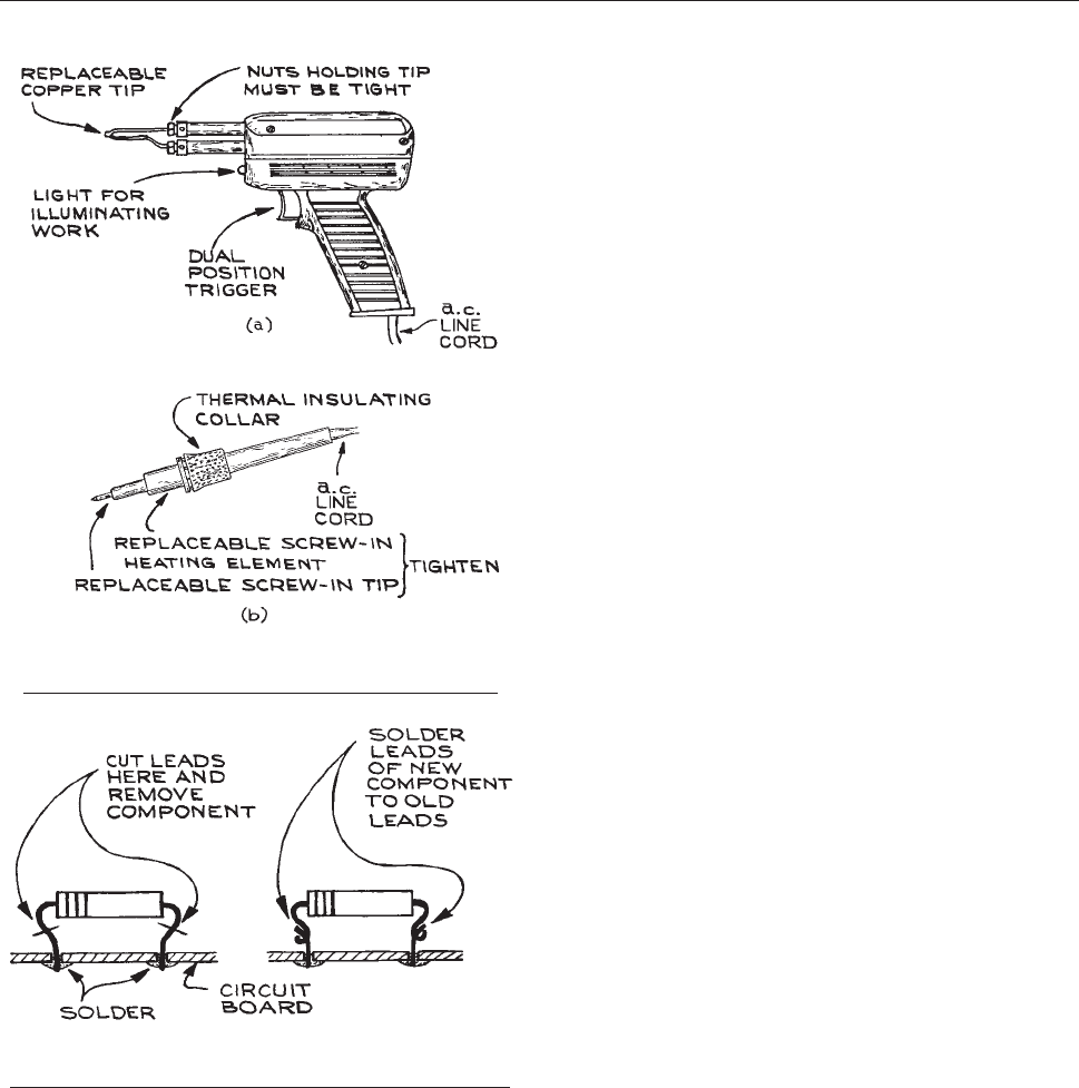
shaped to heat all leads simultaneously. These tips often do not
heat up evenly, resulting in nonuniform heating of the compo-
nent leads. If the component is lifted before all leads are free,
the circuit-board traces can be damaged. After removal of the
component, the holes must be cleaned of residual solder
before proceeding with the insertion of another component.
Solder removal by heating followed by shaking or blowing
should be avoided. It results in solder splashes that can cause
short circuits. Surface-mount components can be removed in a
variety of ways. The simplest is to use solder braid to remove
as much solder from each of the leads as possible and then
heat each lead until the solder is melted and pry it away from
its pad with a fine dental pick. When this is done to all the
pads, the component can be removed from the board. This
method results in the bending of all the component leads and
may lift the pads from the board. Printed circuit-board tracks
that hav e been damaged by overheating or mechanical stresses
can be removed with a knife and replaced with ne w sections
soldered directly to undamaged foil. When pads become
detached from the substrate, they can be replaced with new
ones anchored to the board with swaged eyelets.
An alternative removal method uses a length of music
wire that is inserted behind the leads of the surface-mount
component. As each pin is heated the wire is slid under it to
free it from the pad. This is done for each of the leads until
the component is freed from the board. Because the force
on the wire is parallel to the surface of the circuit board, the
chance of lifting pads and traces is reduced.
When a large number of surface-mount components are
to be soldered, a hot-air rework station gives faster and more
uniform and reliable results that hand soldering with a fine-
tip iron. Such rework stations consist of a source of hot air, a
hand piece or holder, and a set of nozzles. The openings in
the nozzles match the position and size of the contacts of the
surface-mount component to be soldered. With these units,
the temperature, air-flow rates, and duration of air flow can
be separately controlled. The surface-mount components
are placed on the circuit-board pads, which have been coated
with solder paste. The appropriate nozzle is inserted into the
hand piece and the air-flow rate, temperature and flow dura-
tion selected. The nozzle is placed over the component and
the heated air turned on. All contacts are heated simultane-
ously to the temperature at which the solder flows and the
component contacts are bonded to the circuit-board pads. In
a few seconds all connections are made. The procedure is
repeated for all of the components. The more advanced units
allow for programming of air flow, air temperature and
heating cycle. Control over lead temperature and heating
time means that there is no damage to the component nor
to the circuit board. The rework station can also be used to
Figure 6.145 (a) Soldering gun; (b) single-element
soldering pencil.
Figure 6.146 Replacing a component on a printed circuit
board.
522 ELECTRONICS
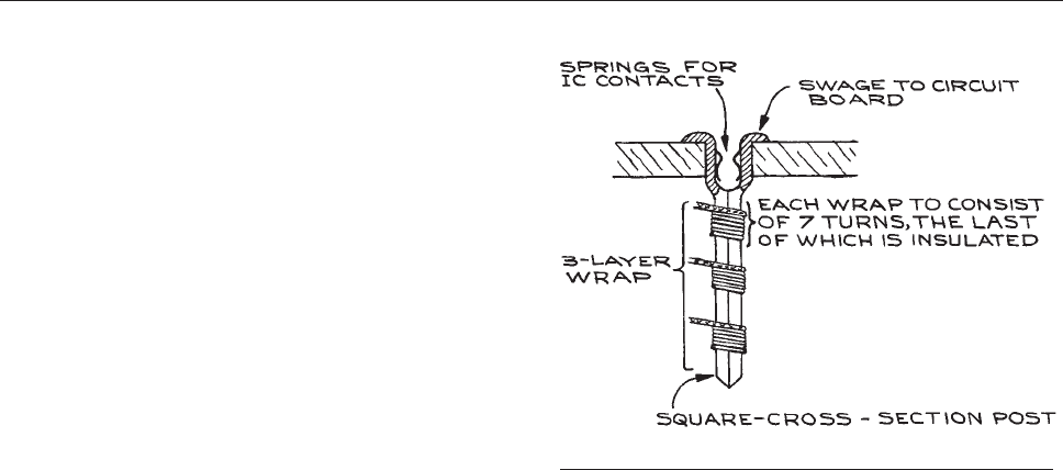
remove surface-mount components from circuit boards by
heating the contacts with the correct size nozzle and remov-
ing the component once the solder holding the contacts
becomes molten. Some rework stations incorporate vacuum
tweezers into the hot-air nozzles to assist in the removal of
the components. Because of the small size of surface-mount
resistors and capacitors, and the fine pitch of surface-mount
IC contacts, a low-power binocular microscope is very use-
ful for assessing the quality of the solder joints and inspect-
ing for solder bridges between contacts.
In the preceding discussion of PCBs, low-frequency
applications have been assumed. If the board is made for
high-frequency applications, a great deal more care is
required in component placement and lead geometry. For
fast logic circuits using ECL ICs, microstrip line geome-
tries are recommended.
17
6.10.4 Wire Wrap
TM
Boards
Boards, made by the Gardner–Den ver Company under the
trade name Wire WrapÔ, have sockets spaced at intervals
corresponding to the spacing of the leads on inte grated cir-
cuits. The sockets have long, square cross-section posts, so
that when the socket is swaged into a substrate material the
post extends on the back-side. The length of the post deter-
mines how many separate connections are to be made to it.
Three- and four-layer length posts are the most common (see
Figure 6.147). A special wrapping tool is used to
make
connections to the pins. The tool can be manual,
line-operated, battery-operated, or air-operated. The hand
tool is entirely adequate for circuits with up to 10 ICs. As
the wire is wrapped around the post, the high pressures gen-
erated between the wire and the sharp corners of the post
form a cold weld, which has good electrical and mechanical
properties. The advantages of such a system are:
(1) No solder connections to cause heat damage to com-
ponents and circuit board
(2) Electrical components that plug into sockets and are
easily removed for replacement or testing
(3) Higher component density than obtainable with double-
sided circuit boards, because wire crossings are possi-
ble without short circuits
(4) Ease of removing and remaking connections (an
unwrapping tool that is a companion to the wrapping
tool allows one to remove connections – however, if the
connection that one wants to remove is not the highest
of a stack, one must remove the upper ones to get to it).
(5) No artwork, photographic reproduction, masking, or
etching required
(6) Reliability
(7) Speed of fabrication
In practice, one uses single-conductor wire specially made
for wrapping. The three most common gauges are AWG 30
(0.25 mm), 28 (0.32 mm), and 26 (0.40 mm). Different wrap,
unwrap, and insulation-stripping tools are used for each
gauge. One can obtain the wire in rolls or in precut and
prestripped lengths. If one uses rolls, it is necessary to have
a wire stripper to remove 1 in. of insulation at either end of
the length of wire to be wrapped. Thermal strippers ensure
that the conductor will not be nicked when stripped, but
special mechanical strippers that do an adequate job can also
be obtained inexpensively.
The usual Wire WrapÔ board consists of a matrix of
sockets with spacing corresponding to the spacing of the
terminals on the normal 14- or 16-pin DIP IC. After the
placement of ICs on the board has been decided upon, a
Wire WrapÔ list is made, which indicates the pins between
which connections are to be made. Each pin is identified by
a letter plus number code identifying the column and row of
the pin [see Figure 6.148(b)]. Once the list is complete, all
the
wrapping can be done at one time. It is common for
Wire WrapÔ boards to have a ground plane and a power-
Figure 6.147 Wire Wrap
TM
post.
HARDWARE AND CONSTRUCTION 523
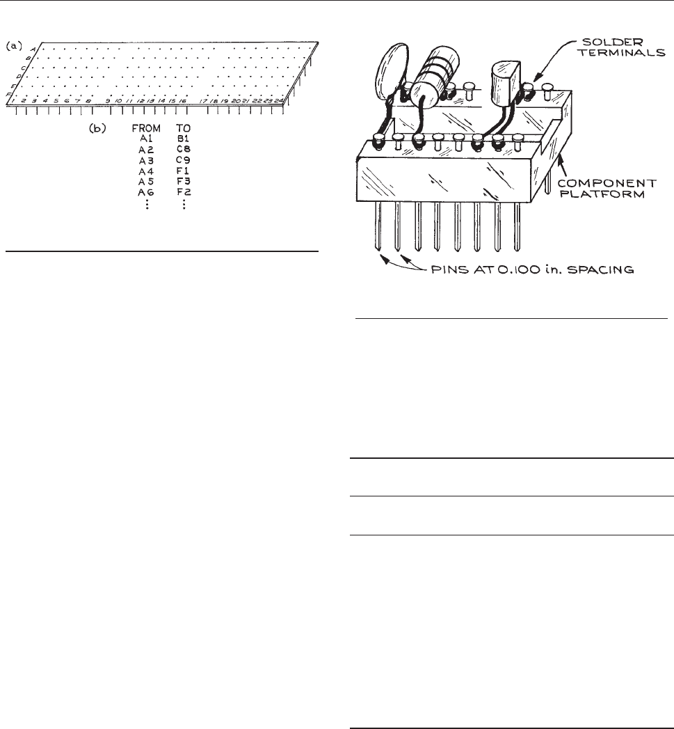
supply voltage plane or bus. The Wire WrapÔ posts can be
connected to these planes at intervals of 14 to 16 pins. A
solder bridge can sometimes be made between the appro-
priate pin and the exposed ground plane. Connections to the
plane from outside the board can be made with a screw-
and-lug connection to tie points on the board. Signal con-
nections are usually via ribbon connectors to DIP sockets.
Discrete components are used with mounting plat-
forms or, if sufficient space is available, they can be
wrapped directly to t he posts. The platforms have pins
that fit the socket holes in the board, and the discrete
components are soldered to the posts or forked terminals
on the top of the platform (see Figure 6.149). When a
circuit
with only a few ICs must be constructed, an inex-
pensive method is to use individual Wire WrapÔ sockets
and glue them to perforated circuit board with 0.100 in.
hole-spacing. This is much less expensive than commer-
cial boards and entirely adequate for low-frequency
applications. A disadvantage of Wire Wrap Ô boards is
their high initial cost, but they can be reused.
Initial verification of the connections on a board is
done by removing all components, attaching the ground
and power-supply leads, and measuring the voltage at each
pin. They should all be consistent with the W ire WrapÔ list.
6.10.5 Wires and Cables
There are many types of electrical wires used in the labo-
ratory. Selection of the correct type is important for cor-
rectly functioning equipment. Wire should be selected
according to its voltage and current rating for routine low-
frequency operation. For applications involving high fre-
quencies and low signal levels, more care must be taken.
The use of multiple-conductor cables can simplify wiring,
Figure 6.148 (a) A Wire Wrap
TM
board; (b) example of a
wrap list.
Figure 6.149 Platform for mounting discrete components.
The platform plugs into the Wire Wrap
TM
board.
Table 6.48 Current-carrying capacities of copper-
insulated wire
B&S Gauge Diameter (in.) Allowable
Current
a
(A)
Resistance
per 100 ft.
b
(X)
8 0.128 50 0.628
10 0.102 30 0.999
12 0.081 25 1.588
14 0.064 20 2.525
16 0.051 10 4.016
18 0.040 5 6.385
20 0.032 3.2 10.15
22 0.025 2.0 16.14
24 0.020 1.25 25.67
26 0.016 0.80 40.81
28 0.013 0.53 64.90
30 0.010 0.31 103.2
a
For rubber-insulated wires the allowable current should be
reduced by 30%.
b
At 20 °C (68 °F).
524 ELECTRONICS

and some knowledge of the kinds of multiple conductor
configurations is useful. Table 6.48 lists the diameter, allow-
ab
le current, and resistance per 100 feet of B&S-gauge
insulated copper wire. Table 6.49 lists the electrical proper-
ti
es of common thermoplastics used for insulation.
The most common wire is a.c. line cord, the type used for
connection to the a.c. outlet. Twin-conductor zip cord should be
avoided in laboratory applications because of its limited resist-
ance to mechanical stresses. Three-conductor color-coded line
cord is best suited for the laboratory . The double insulation of
Table 6.49 Electrical properties of thermoplastics
Material Trade Name Volume
Resistivity
(X cm)
Dielectric
Strength
(V/mil)
a
Power Factor
at 60 Hz
Characteristics
ABS Lustran 10
15
–10
17
300–450 .003–.007 Tough, average overall electrical
properties
Acetals Delrin 10
14
500 .004–.005 Strong, good electrical properties to
125 °C
Acrylics Lucite, Plexiglas,
Perspex
>10
14
450–480 .04–.05 Resistant to arcing
Fluorocarbons:
CTFE KEL-F 10
18
450 .015 Excellent electrical properties, some
cold flow
FEP Teflon FEP >10
18
500 .0002 Properties similar to TFE, good to
400 °F
TFE Teflon TFE >10
18
400 <.0001 One of the best electrical materials
to 300 to 500 °F, cold flow
Polyamides Nylon 10
14
–10
15
300–400 .04–.6 Good general electrical properties,
absorbs water
Polyamide-imides
and polyimides
Vespel, Kapton 10
16
–10
17
400 .002–.003 Operating temperatures from 400
to 700 °F, excellent electrical
properties
Polycarbonates Lexan 10
16
410 .0001–.0005 Good electrical, excellent
mechanical properties, low water
absorption
Polyethylene and
Polypropylenes
—10
15
–10
18
450–1000 .0001–.006 Good electrical, weak mechanical
and thermal properties
Polyethylene
terephthalates
Mylar >10
16
500–710 .0003 Tough, excellent dielectric
properties
PVC Saran 10
11
–10
16
300–1100 .01–.15 Low cost, general purpose, average
electrical properties
a
mil ¼.001 in.
HARDWARE AND CONSTRUCTION 525
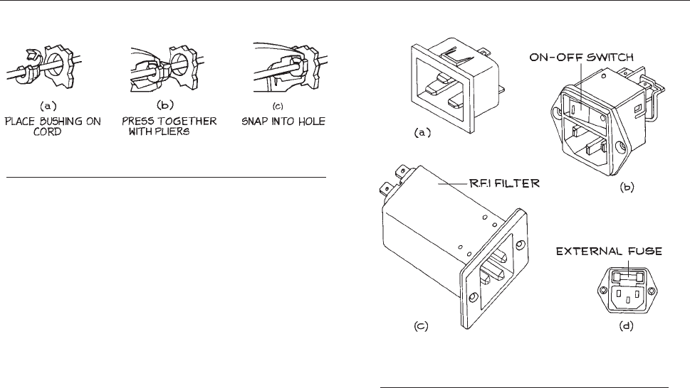
the wires provides extra mechanical and electrical protection.
The standard code is black for hot, white for neutral, and green
for ground, and should be observed at both the plug and the
chassis end of the cord. T o minimize damage to the line cord at
the chassis end, strain relief and mechanical protection of the
insulation should be provided. This is often accomplished with
a single strain-relief grommet or combination plastic grommet
and clamp, as in Figure 6.150. An alternativ e to direct con-
nection
of an a.c. line with plug to a chassis is an a.c. r eceptacle
or power entry module. These accept standard a.c. line cords
with male connectors on the a.c. outlet end and female con-
nectors that mate to the receptacle or module. The receptacles
and modules may contain on–off switches, fuses, pilot lights,
and r .f.i filters. Some examples are sho wn in Figure 6.151.
Line
cord is almost always stranded to enhance flexibil ity.
If the wire is to be used in high-current-carrying applications,
care should be taken not to cut the strands when stripping,
since that will limit the current carrying capacity of the wire
and cause heating at the stripped end. Sometimes the indi-
vidual strands are insulated with varnish. When making elec-
trical connections with wire of this kind, the insulation must
be removed with fine emery paper or steel wool.
Another type of wire used for a.c. lines is the solid-con-
ductor #12 or #14 gauge wire for po wer distribution. The most
common are two- and three-conductor Romex, which is PVC-
insulated, and two-conductor BX, which has a metal-armored
outer covering. Both types can be routed within walls in either
metal or PVC conduit. Because of the heavy gauge of the
conductors, connections are made to screw terminals or with
wir e nuts when splices are invo lved. The installation of a.c.
lines requires a professional electrician who knows the con-
ventions, regulations (codes), and procedures for fusing and
connection to existing po wer lines.
For electronic circuits where the voltages are less than
a few hundred volts and the curre nts are a few amperes,
hookup wire is u sed. This can be solid conductor or
multistranded. The solid-conductor wire is easier to
use when making connections because it does not fray,
but it lacks the flexibility of multistranded wire. Hookup
wire is generally tinned – that is, coated with a tin–lead
alloy to enhance solderability. The insulation is usually
PVC, polyethylene, or TeflonÔ.
When stripping wire, care should be taken to avoid
nicking the conductor of solid wire and cutting strands
of multistranded wire. There are a large variety of wire
strippers on the market (see Figure 6.152), but none is
foolproof
and all require a certain amount of skill if the
conductor is to remain undamaged. Thermal strippers that
melt the insulation locally before it is withdrawn from the
wire work very well, but are not portable. For TeflonÔ-
insulated wire, thermal strippers are very useful because
the slippery material is difficult to grip.
When working with stranded wire, it is recommended
that the ends be tinned. It should be remembered, however,
that solder will render multistrand wire rigid, so tinning
should be confined to a short length at the end. For coding
purposes, the insulation of hookup wire comes in many
Figure 6.150 Mounting line cord at the chassis to relieve
strain on the electrical connections.
Figure 6.151 A.c receptacle/power line modules:
(a) simple; (b) on–off switch incorporated;
(c) with internal r.f.i. protection; (d) external fuse.
526 ELECTRONICS
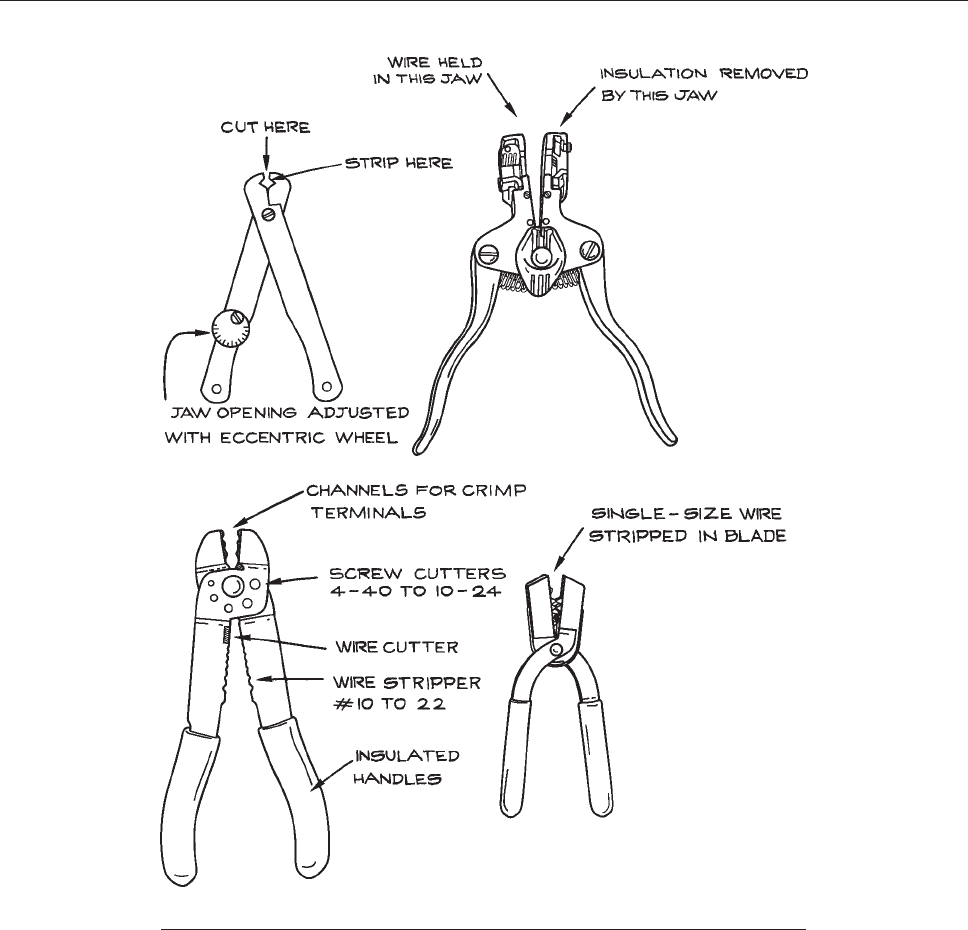
colors and combinations of colors. Color coding is a very
useful way to avoid wiring errors and makes subsequent
troubleshooting easier.
Test-prod wire is highly flexible multistrand wire with
rubber insulation rated at a few thousand volts. Such wire
comes with red or black insulation and is used with multi-
meters and in high-voltage circuitry.
For voltages from a few kilovolts to several tens
of kilovolts, special high-voltage cable must be used.
The most common jacket materials are silicone rubber,
TeflonÔ, and KaptonÔ. Silicone-rubber insulation is very
flexible, but has only modest dielectric breakdown strength
and volume resistivity, so that high-voltage cables made
with it have large diameters. KaptonÔ, a polyimide, has
Figure 6.152 Wire strippers.
HARDWARE AND CONSTRUCTION 527

high breakdown strength and volume resistivity, and cables
made with it are relatively small in diameter. Stiffness is
the principal disadvantage of KaptonÔ. The properties of
TeflonÔ are intermediate between those of silicone rubber
and KaptonÔ, and it is usually the best compromise. Typ-
ical properties of high-voltage TeflonÔ cable are given in
Table 6.50. One source of high-voltage cable is the ignition
cables
used in automobiles. The silicone-rubber-insulated
stainless-steel or copper stranded-conductor type found in
high-performance cars can be used to 50 kV. The more
common carbon-filament conductor cable used to mini-
mize r.f.i. is not suitable.
Magnet wir e is varnish-insulated, solid-conductor wire
used for winding electromagnets, transformers, and induc-
tors. The thin insulation means that a large number of turns
can be packed into a given volume. To make electrical con-
nections with such wire, the varnish must be removed with
emery paper, steel wool, or special solvents. Magnet wire is
not a suitable substitute for hookup wire. When using it for
electromagnets, one should be aware of the possible buildup
of heat around the inner windings, which can degrade the
insulation and create short circuits. The varnish insulation is
rated for voltage break-down and heat resistance.
For high-current electromagnets, rectangular cross-
section wire is used, because the high surface-area-to-
volume ratio facilitates convection cooling. In applications
that require conduction cooling, hollow-core wire is used,
through which cooling water can be circulated.
In addition to two- and three-conductor line cord, there
are many other multiconductor, round-cable configurations.
The conductors can be solid or stranded. The wires are
color-coded for identification. For low-level, low-frequency
signals, the wires can be enclosed in a single shield, as is
done for microphone cable. Configurations where there is
individual shielding of single wires also are available.
Shielding can be in the form of a braid or a foil – if it is
foil, a drain wire is also included, which is electrically
connected to the shield and to which connections can be
made. For high-frequency applications there is coaxial
cable and 300 X, parallel-conductor cable with transmis-
sion-line properties. These are discussed in the sections
on coaxial cable and connectors (Sections 6.2.3 and 6.2.4).
Flat
multiconductor cable is very useful when a large
number of wires are needed, as with computer and data inter-
faces. There are many different arrangements of the wires
within such cable. The most common consists of round par-
allel conductors. There are also flat conductors and alternat-
ing round and flat conductors. Flat conductors minimize
interconductor capacitance and interference among signals.
Twisted pairs of wires are used for transmission lines because
constant impedance can be maintained and the wires are
flexible and easy to route. An alternating twisted pair–straight
geometry is often used for data transmission. The great
advantage of flat cable is that mass termination insulation
displacement connectors can be used. These connectors are
designed so that the cable is clamped and electrical contact is
made to each of the wires in a single operation with a special
tool. No stripping, soldering, or crimping is required. The
reliability of such connections is e xcellent.
6.10.6 Connectors
Probably the best-kno wn connector combination is
the binding post and banana plug or tip plug (see Fig-
ur
e 6.153). A wide variety of conductors and conductor
te
rminations can be made to binding posts in a rapid, reli-
able semipermanent manner. Binding posts have the disad-
vantage of being bulky and highly susceptible to the pickup
and radiation of electromagnetic energy. When mounting
binding posts on a chassis, the mounting hole should be
made large enough to accommodate the shoulders on the
insulating sleeves. In this way, the central conductor is kept
well away from the chassis. The standard spacing between
posts is 0.75 in. This corresponds to the spacing of twin-
conductor banana plugs (see Figure 6.154), which are quite
co
mmon and useful, especially when it is necessary to
Table 6.50 Typical high-voltage Teflon-insulated cable
d.c. Voltage
Rating
a
(kV)
Conductor Cable Diameter (in.)
10 19/36
b
0.077
15 0.097
20 0.117
25 0.137
40 0.197
50 0.237
a
a.c. voltage rating is typically 20–25% of d.c.
b
19 strands of #36 wire.
528 ELECTRONICS
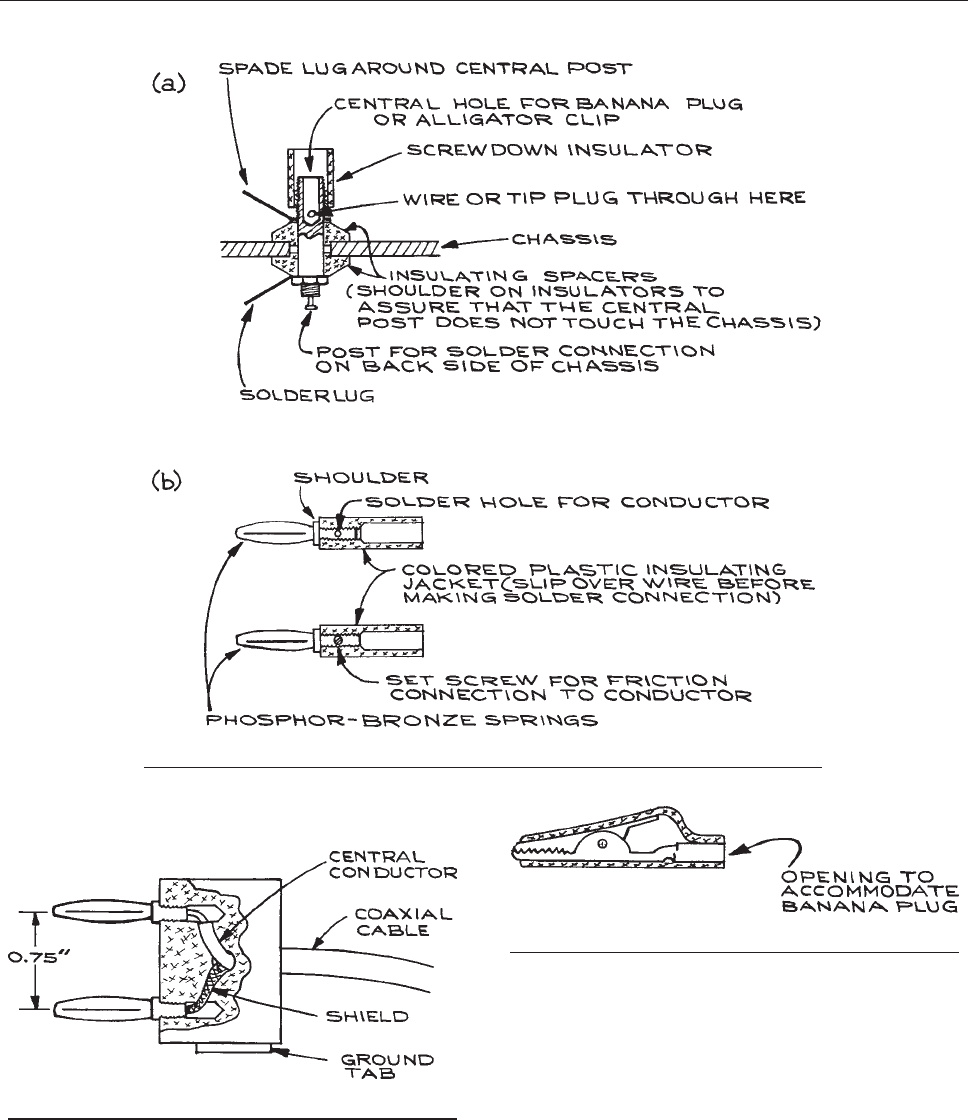
connect coaxial cable to binding posts. The twin plug usu-
ally has one terminal marked ground, to which the shield of
coaxial cable is attached.
Alligator clips (see Figure 6.155), although useful with
test
leads, should not be used in any permanent or even
semipermanent installation. The type of clip into which
Figure 6.153 (a) Binding post; (b) banana plug.
Figure 6.155 Alligator clip with insulated plastic cover.
Figure 6.154 Twin-conductor banana plug.
HARDWARE AND CONSTRUCTION 529
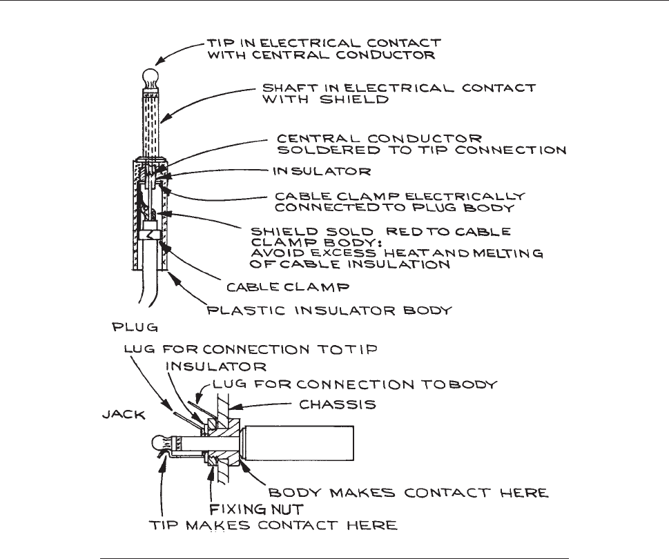
one inserts a banana plug is more useful than a clip requiring
solder or screw connections. Flexible insulating sleev es that
fit over the clips prev ent short circuits and are always used
when the clip is at the end of a test lead.
Phone plugs (see Figure 6.156) come in several different
s
izes and provide one means for the termination and con-
nection of coaxial cable carrying low-frequency signals.
Because this type of plug is polarized (that is, the connec-
tions can only be made in one way), it is sometimes used for
low-voltage, low-current d.c. power-supply connections.
There are many variations on the basic plug–jack design.
There are plugs that can accommodate three or more sepa-
rate connections, and there are jacks that remain shorted
until the insertion of the plug.
Insulated barrier strips (see Figure 6.157) with screw
terminals
are a good way of making semipermanent con-
nections for d.c. applications, and are often found on the
rear panels of power supplies.
For terminating the ends of wires, there are a variety of
terminal connectors that can be attached to the wire by sol-
dering or crimping (see Figure 6.158). The terminal used
should
be of the correct size with respect to both the wire
Figure 6.156 Phone plug.
530 ELECTRONICS
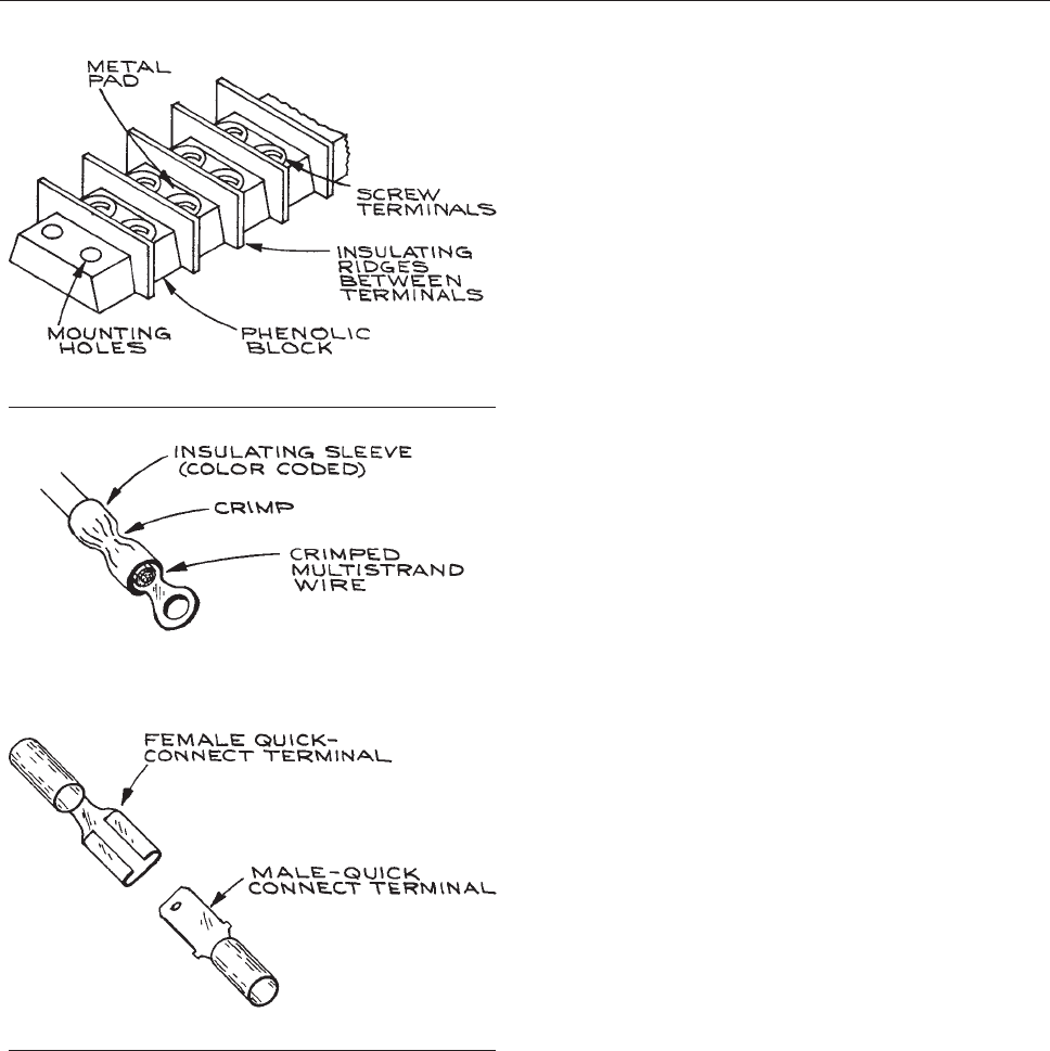
used and the opening at the end. Quick-connect, friction-type,
push-on terminals are very useful in d.c. applications, when
the connection must be repeatedly made and broken. Such
terminals are often also found on mechanical relays, circuit
breakers, and mechanical switches. Crimp connectors are
color-coded according to the wire-size range they can accom-
modate. It is important to use the proper crimp-tool opening –
color-codedonmanytools–toavoidtoolooseacrimp(too
large a hole) or a severed wire (too small a hole). Three
diff erent typ es of crimping tool are show n in Figure 6.159.
Wh
en soldering connectors, only enough heat should
be used to make a good joint, since too much heat will melt
the insulation. Some type of third hand is helpful in this
regard – a small vice or an alligator clip at the end of a heavy
piece of solid copper wire anchored to a metal base.
A very large part of the electronics-har dware indus-
try is devoted to the manufac ture of connectors. For
laboratory applications, only a few of the most com-
mon ones will be described, and some guidelines for
connector s election will be given. Electrical c ontacts
between the wires and connector pins can be made by
soldering or crimping. For some connectors, the pins
must be re moved to make the electrica l connection
and then i nserted into the connector block. Removal
of the pin then requires a special tool. A common
power connector using crimped sockets and pins is
shown in Figure 6.160. High -density conn ectors using
c
rimped t erminals and integral holding latches are
shown in Figure 6.16 1.
D-connectors
derive their name from the cross-sectional
shape of the connector body (see Figure 6.162). The usual
RS
232C interface uses a 25-pin, subminiature D-connector.
The connector can have up to 50 contacts and connection is
made in a variety of ways: by soldering the conductors into
a hollow recess at the back of the contact (solder pot); with
crimp pins and sockets; and with ribbon-cable mass termi-
nation contacts. Such connectors can be attached directly
to a panel with the correct cutout. When fitted with a shell
(either plastic or metal) and a cable clamp, they become
plugs. Locking accessories are also available for securing
the plug to the mating jack, and the D-shape assures cor-
rect mating. Double-density connectors of this type are
also made, and there exist a wide variety of configurations
with high-voltage, high-current, and coaxial contacts, in
addition to the standard single pins. Because pins are very
closely spaced, shrink tubing is routinely used over the
solder connections. This tubing comes in a variety of sizes,
materials, and shrink ratios. When used to insulate solder
connections, the tubing serves a strain-relief as well as an
insulating function. It is important to choose the correct
Figure 6.158 Wire terminals.
Figure 6.157 Barrier strip.
HARDWARE AND CONSTRUCTION 531
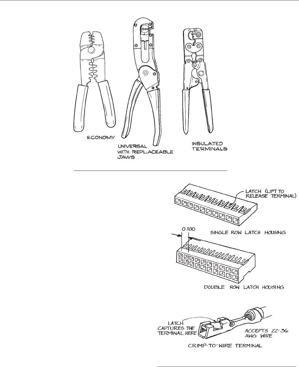
diameter tubing for the application. If the tubing is too
small in diameter, it will split upon being shrunk over
the enclosed wire or connector – if the diameter is too
large, it will not fit tightly. Heating should be done with
a heat gun rather than a soldering iron.
Threaded circular connectors (see Figure 6.163)are
ba
sed on designs originally used by the military for aircraft.
They employ separate removable pins and a threaded mat-
ing collar to make a mechanically secure union between
male and female connectors. There is a broad range of sizes,
styles, and pin arrangements, and for this reason these con-
nectors are used on a variety of laboratory electronic equip-
ment. There are various ways of retaining the pins in the
insulator block. Some of them require special insertion and
removal tools, while others use a second backup block held
in place inside the connector.
Nuclear instrumentation module (NIM) and CAMAC
equipment are examples of the connection of a modular elec-
tronic unit to a main chassis. The basic connector is a rec-
tangular insulator block, which holds contact pins maintained
in place by one-way spring action. Wires are crimped to the
Figure 6.159 Crimping tools.
Figure 6.160 Multiple contact connector, crimp terminals,
insertion/extraction tool.
532 ELECTRONICS
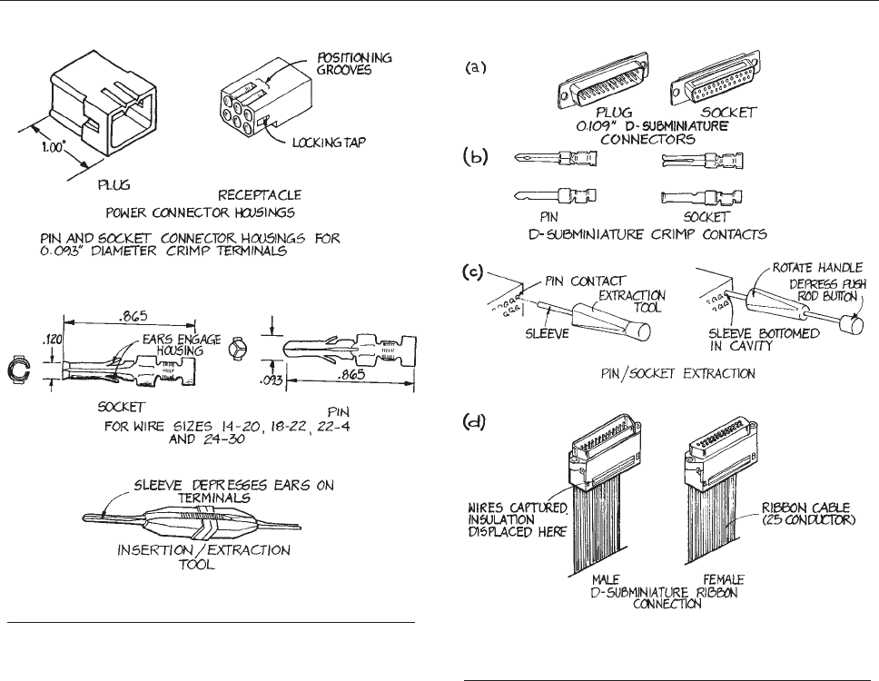
pins that are then inserted into the block. An extraction tool is
required for pin removal. When the connector has a large
number of pins, considerable force is required for mating
and threaded screw jacks are often used. Extra pins can be
purchased separately and shrouds are av ailable to con v ert the
connector to a plug.
No high-voltage connector is entirely satisfactory, and
forthisreasontheyshouldbeavoidedandpermanent
connections with ceramic feedthroughs or standoffs
made whe never possible. Reynolds/Teledyne manufac-
tures a wide range of single-conductor, multiple-conduc-
tor an d co-axial high-voltage wire and c onnector s with
voltage ratings to 70 kV. European-type phenolic spark-
plug connectors ma ke acceptable connectors when used
with ignition cable; a drilled-out Teflon Ô-insulated r.f.
coaxial connector can a lso be used. These are illustrated
in Figure 6.16 4.
6.11 TROUBLESHOOTING
6.11.1 General Procedures
There are a number of steps that can be taken when a piece
of electronic equipment fails to operate properly. These
depend on the complexity of the equipment and the avail-
ability of test equipment and diagrams.
The worst symptoms are usually the easiest to treat. An
experienced TV repairman once noted that 95% of all
Figure 6.162 (a) D-connector; (b) pin and socket crimp
contacts; (c) pin and socket extraction with tool;
(d) ribbon-cable connections.
Figure 6.161 Multiple conductor connector and crimped
terminal.
TROUBLESHOOTING 533
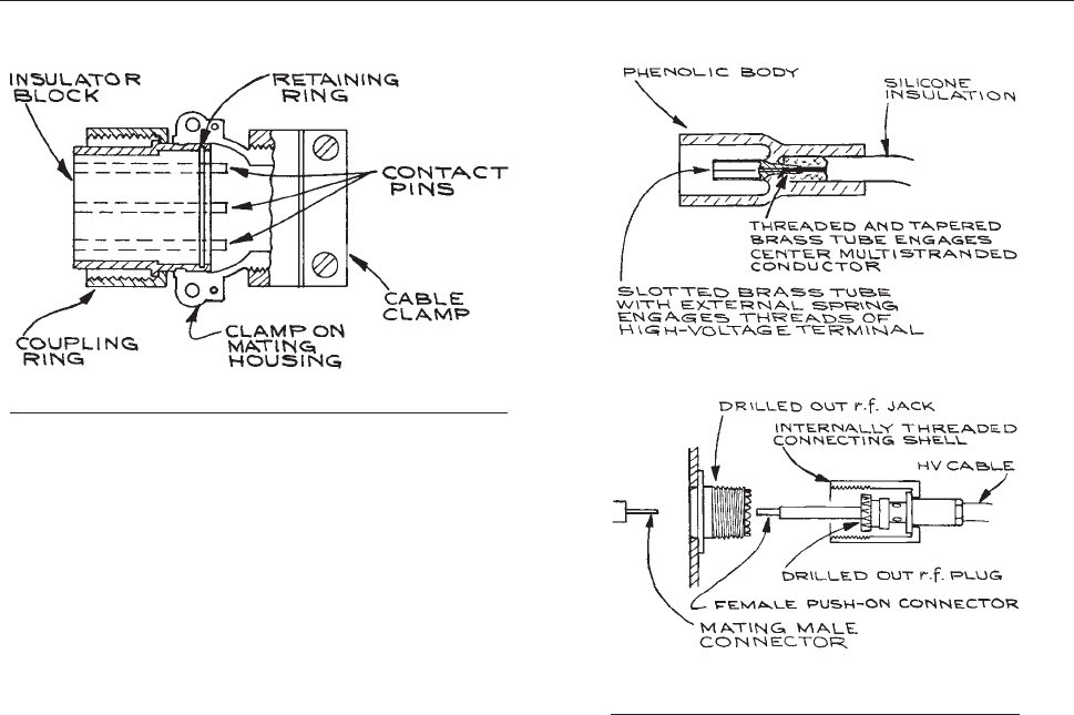
malfunctions in TV sets could be found and corrected in
less than one half hour. For the other 5% the best solution
was to sell the customer a new set. This also applies to
laboratory equipment. With increasing use of highly reli-
able integrated circuits and resistance and capacitance
modules, the most unreliable elements of a circuit are
the mechanical parts (such as switches, dials, and fans)
and especially the connectors. When an amplifier or power
supply no longer works, one’s first impulse should not be
to take out screwdriver and wrench and begin disassem-
bling the chassis, but to be sure that it is plugged in, that the
on–off switch is functioning, that all fuses are intact, that
the cooling fans are operating, and that the air filters are
clean and not blocked. Switch contacts can be cleaned with
spray cleaners made for the purpose. If these measures
produce no results, the various dial and switch settings of
the instrument should be checked. Often what is viewed as
a malfunction is merely an incorrect setting, causing the
instrument to operate in an unexpected mode.
If these simple actions are not effective, the next course
of action depends on the complexity of the equipment and
the availability of circuit diagrams. To repair a complex
circuit without circuit diagrams is almost impossible. If
diagrams are not at hand, the manufacturer should be
contacted for the necessary diagrams and troubleshooting
procedures. Often these are available online, so a web
search is a good way to begin.
There are, of course, certain visual checks that one can
perform without knowledge of the circuit. Charred resis-
tors and an overheated circuit board are readily apparent,
as are loose and dangling wires. One difficulty with merely
replacing a damaged component, however, is that only the
symptom may be treated. The charred resistor may be the
result of a failure in another component.
Troubleshooting is most effective and efficient when a
complete set of circuit diagrams, schematic drawings,
chassis diagrams, and functional block diagrams are avail-
able. These are often accompanied by a troubleshooting
guide, which lists the most frequently encountered mal-
functions, the symptoms, and the remedies. The area in
which the malfunction is occurring can often be localized
by studying the functional block diagram of the unit. As an
example, consider a counter-timer that responds normally
to input signals but gives erratic readings when counting
for preset time intervals, and erratic times when in the
preset-counts mode. In this case, the gating circuit and
Figure 6.164 High-voltage connectors made
from a spark-plug and r.f. connector.
Figure 6.163 Threaded military-type connector.
534 ELECTRONICS
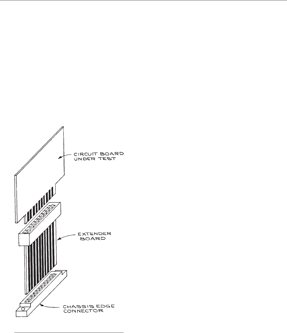
the time base are obviously suspect. One should begin by
looking at that part of the circuit.
Good schematic diagrams include waveforms and volt-
age levels at all critical points in the circuit. These should
be checked first. Well-designed circuit boards often have
the d.c. voltage levels printed directly at the appropriate
test points and components identified by a printed letter-
and-number code that corresponds to an identical code on
the schematic diagram.
A common difficulty is gaining access to components and
connections in the restricted space between boards in a
multiple circuit-board assembly. Extender boards (see
Figure 6.165)arecircuitboardsarrangedinsuchawaythat
th
ey mate to the circuit-board connector at one end and the
circuit board itself at the other end. The extender board is of
sufficient length to place the board in a position where the
components and circuit interconnections are easily accessi-
ble. Signal injection is a common method for isolating a
circuit fault. With this technique, an appropriate signal is
injected at the input of the suspected circuit element, and the
output is monitored. This works well for linear circuits, such
as amplifiers, but becomes quite complex for digital circuits,
where it may be necessary to stimulate several input termi-
nals and monitor several output terminals simultaneously –
and often in synchronization with a clock signal. Logic
pulsers, probes, and clips, are useful for small-scale testing.
They are shown in Figure 6.166. For more complex circuits,
it
is necessary to capture the signals and store them for
subsequent analysis. There are logic analyzers made expres-
sly for this purpose. They are expensive, however, but
worthwhile in situations where a large amount of digital
circuit troubleshooting is done – more the domain of the
electronic technician than the experimental scientist. Often
it is much more economical to replace all the suspected ICs
in a given section (especially if they are easily removable
and in sockets) than to test each one individually.
Some common sources of faults in electronic equipment
are:
(1) Electrolytic capacitors in general
(2) Pass transistors in the output circuit of power supplies
(3) Input transistors in the input circuits of amplifiers and
preamplifiers
(4) Mechanical switches and potentiometers.
Repeated failure of input transistors in low-level pream-
plifier circuits can often be cured by placing two diodes,
such as lN914s, across the input, as shown in Figure 6.167.
So
long as the input signal does not exceed a few tenths of
a volt, both diodes remain nonconducting, allowing the
unattenuated signal to pass. Should the signal exceed
0.6 V – positive or negative – one or the other diode will
conduct, shunting the signal to ground and protecting the
input from excessive voltage levels.
6.11.2 Identifying Parts
One can often localize the malfunction to a circuit compo-
nent, but may not know enough about the component to be
Figur e 6.165 Use of the extender board for trou-
bleshooting.
TROUBLESHOOTING 535
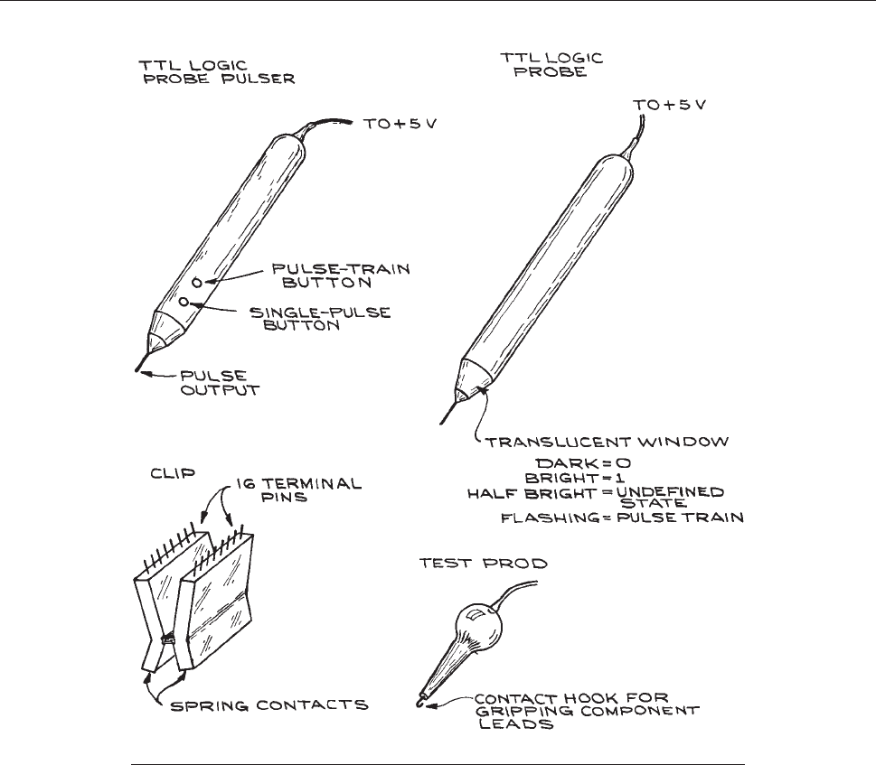
able to replace it. The parts list may gi v e the equipment
manufacturer’s component code rather than the standard
code of the component manufacturer . When this is the case,
it is necessary to identify the component from the code
printed on it. Most ICs, transistors, and other components
have a four-digit date code gi ving the date of manufacture.
The first two digits are the year, and the next two are the
week of the year. Thus, 9812 is the 12th week (last week in
April) in 1998. The other codes are the manufacturer’s com-
ponent designation. To help identify the manufacturer, a list
of logos can be found at the follo wing web sites: http://
www.icmaster.com/LogosA-M.asp and http://www.icmaster.
com/LogosN-Z.asp. The site http://www.elektronikforum.de/
ic-id has links to icmaster and others. Semiconductor
manufacturer homepages and data sheets are given at http//
www.bgs.nu/sdw/p.html. A list of the prefix codes of
semiconductor manufacturers is gi v en in Table 6.51.Once
the
manufacturer is known, the appropriate data book or web
Figure 6.166 Logic pulser, probe, clip, and test prod.
536 ELECTRONICS
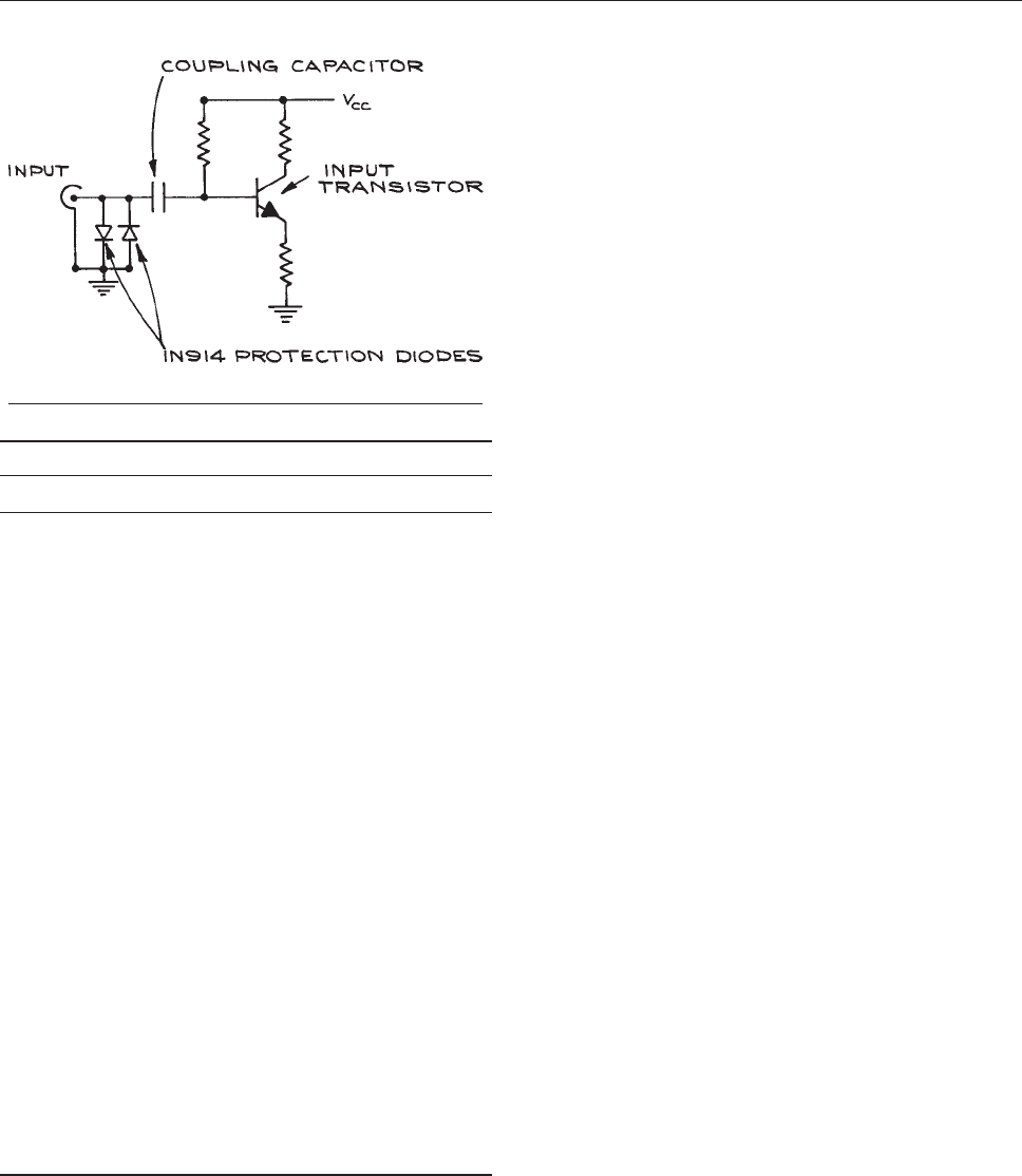
site can be consulted. One should replace components with
caution, paying attention to the package type and temper -
ature range. The three standard ranges are commercial (0 to
70 °C), industrial (25 to þ85 °C), and military (55 to
þ125 °C). Sometimes specially selected or matched compo-
nents are used. Replacement with off-the-shelf units may not
work in this case.
Cited References
1. H. W. Bode, Network Analysis and Feedback Amplifier
Design, Van Nostrand, Princeton, NJ, 1945.
2. Electr. Design, 24, 63, 1976.
3. J. Millman and C. C. Halkias, Integrated Electronics:
Analog and Digital Circuits and Systems, McGraw-Hill,
New York, 1972, pp. 244–245.
4. J. G. Tobey, G. E. Huelsman, and L. P. Graeme, Operational
Amplifiers, Design and Application, McGraw-Hill, New
York, 1971; J. Graeme, Designing with Operational
Amplifiers, McGraw-Hill, New York, 1977.
5. E. Fairstein and J. Hahn, Nuclear pulse amplifiers –
fundamentals and design practice, Nucleonics, 23(7 ),
56, 1965; Nucleonics, 23(9), 81, 1965; Nucleonics, 23(11),
50, 1965; Nucleonics 24(1), 54, 1966; Nucleonics, 24(3) ,
68, 1966.
6. Voltage Regulator Handbook, National Semiconductor
Corporation, Santa Clara, CA, 1975.
7. FAST Data Manual , Signetics Corp., Sunnyvale, CA, 1984.
8. Standard Nuclear Instrument Modules, adopted by AEC
Committee on Nuclear Instrument Modules, US
Government Publication TID-20893 (Rev. 3).
9. P. H. Garrett, Analog I/O Design, Reston Publishing Co.,
Reston, VA, 1981.
10. S. Letzter and N. Webster, IEEE Spectrum, August, 67–75,
1970.
11. John C. Fisher, Lock in the Devil, Educe Him, or Take Him
for the Last Ride in a Boxcar? Tek Talk, Princeton Applied
Research, 6, No. 1.
12. A. C. Melissinos, Experiments in Modern Physics,
Academic Press, New York, 1966, Chapter 10.
13. R. R. Goruganthu, M. A. Coplan, J. H. Moore and J. A.
Tossell, J. Chem. Phys., 89, 25, 1988.
14. R. Morrison, Grounding and Shielding Techniques in
Instrumentation, John Wiley & Sons, Inc., New York, 1967.
15. Floating Measurements and Guarding, Application Note
123, Hewlett-Packard, Palo Alto, CA, 1970.
16. S. Weber (Ed.), Circuits for Electronics Engineers,
Electronics Book Series, McGraw-Hill, New York, 1977; W.
Figure 6.167 Use of protection diodes at a low-level input.
Table 6.51 Semiconductor integrated-circuit code prefixes
Company Prefix
a
Analog Devices AD
Advanced Micro Devices Am
General Instrument AY, GIC, GP
Intel C, I
RCA CA, CD, CDP
TRW CA, TDC, MPY, CMP, DAC,
MAT, OP
Precision Monolithics PM, REF, SSS
National Semiconductor DM, LF, LFT, LH, LM, NH
Fairchild F, A, lL, Unx
Ferranti FSS, ZLD
GE GEL
Harris HA
Motorola HEP, MC, MCC, MCM, MFC,
MM, MWM
Intersil ICH, ICL, ICM, IM
ITT ITT, MIC
Siliconix L, LD
Fugitsu MB
Mostek MK
Plessy MN, SL, SP
Signetics N, NE, S, SE, SP
Raytheon R, RAY, RC, RM
Texas Instruments SN, TMS
Sprague ULN, ULS
Westinghouse WC, WM
Hewlett-Packard 5082-nnnn
Vishay Si
a
x ¼number; n ¼letter.
REFERENCES 537

Furlow (Ed.), Circuit Design Idea Handbook,Cahner’s
Books, Boston, 1974; Electronics Circuit Designer’s
Casebook, Electronics, New York; Signetics Analog
Manual, Applications, Specifications, Signetics Corporation,
Sunnyvale, CA; Linear Applications Handbook, Vols. 1 and
2, National Semiconductor Corporation, Santa Clara, CA.
17. W. R. Blood, Jr., MECL Applications Handbook, 2nd edn.,
Motorola Semiconductor Products, Phoenix, AZ, 1972.
18. D. Lindsey, The Design and Drafting of Printed Circuits,
2nd edn., Bishop Graphics, Westlake Village, CA, 1984.
19. D. H. Sheingold (Ed.), Transducer Interfacing Handbook,
Analog Devices, Norwood, MA, 1980.
General References
CAMAC and IEEE-488 (GPIB or HP-IB)
CAMAC: A Modular Instrumentation System for Data
Handling, ESONE Committee, Report EUR 4100, 1972,
Chapters 4– 6.
CAMAC Tutorial Issue, IEEE Trans. Nucl. Sci., NS-20 (2), April
1973.
D. Horelick and R. S. Larsen, CAMAC: ‘‘A Modular Standard,’’
IEEE Spectrum, April 50, 1976.
HP-IB General Information, Hewlett-Packard Publication No.
5952–0058.
IEEE Standard 488, available from the IEEE Standards Office,
345 E. 47th St., New York, NY 10017.
Specifications for the CAMAC Serial Highway and Serial Crate
Contr oller Type 62, Report EUR 6100e, Commission of the
European Communities, Greel, Belgium, 1976, Chapter 14.
Circuit Theory
P. Grivet, The Physics of Transmission Lines at High and Very
High Frequencies, Academic Press, New York, 1970.
H. V. Malmstadt, C. G. Enke, and S. R. Crouch with G. Horlick,
Electronic Measurements for Scientists, Benjamin, Menlo
Park, CA, 1974.
J. Millman and A. Grabel, Microelectronics, 2nd edn., McGraw-
Hill, New York, 1987.
C. J. Savant, Jr., Fundamentals of the Laplace Transform,
McGraw-Hill, New York, 1962.
A. I. Zverev, Handbook of Filter Synthesis, John Wiley & Sons,
Inc., New York, 1967.
Printed Circuit-Board Software
Schematic Capture and Board Layout
Electronics Workbench
908 Niagra Falls Boulevard, Suite 068
North Tonawanda, New York
14120-2060
800-263-5552
FAX: 416-977-1818
http://www.electronicsworkbench.com
PADS Software Inc.
165 Forest Street
Marlborough MA 01752
508-485-4300
FAX: 508-485-7171
http://www.pads.com
Ivex Design International
15232 NW Greenbrier Parkway
Beaverton, OR 97006
503-531-3555
FAX: 503-629-4907
WinDraft, WinBoard, IvexView, IvexSpice
Cadence Design Systems
2655 Seely Road
San Jose, CA 95134
1-800-746-6223
FAX: 408-943-0513
http://www.cadence.com
Mentor Graphics Corporation
8005 S.W. Boeckman Road
Wilsonville, OR 97070
1-800-547-3000
http://www.mentor.com/pcb/
P-CAD
12348 High Bluff Drive
San Diego, CA 92130
858-350-3000
FAX: 858-350-3001
http://www.pcad.com
Protel Technologies, Inc.
5252 North Edgewood Drive
Suite 175
538 ELECTRONICS

Provo, UT 84604
1-800-544-4186
FAX: 801-224-0558
http://www.protel.com
Printed Circuit-Board Fabricators
Golden Gate Graphics
South Bay Circuits
Advanced Circuits
21100 East 33rd drive
Aurora CO 80011
http://www.advanced circuits.com
Control Analysis and Design
R. C. Dorf, Modern Control Systems, 6th edn., Addison-Wesley,
New York, 1992.
T. E. Fortmann and K. L. Hitz, An Introduction to Linear Control
Systems, Marcel Dekker, New York, 1977.
G. F. Franklin, D. J. Powell, and A. Emami-Naeini, Feedback
Contr ol of Dynamic Systems, 2nd edn., Addison-Wesley,
New York, 1991.
B. C. Kuo, Automatic Control Systems, 6th edn., Prentice-Hall,
New Jersey, 1990.
K. Ogata, Modern Control Engineering, 2nd edn., Prentice-Hall,
New Jersey, 1991.
C. L. Phillips and R. D. Harbor, Feedback Control Systems, 2nd
edn., Prentice-Hall, New Jersey, 1991.
Components
M. Grossman, Focus on r.f. Connectors, Electr. Design, 24(11),
60, 1976.
C. A. Harper, To compare electrical insulators, Electr. Design,
24(11), 72, 1976.
Handbook of Components for Electronics, C. A. Harper (Ed).,
McGraw-Hill, New York, 1977.
T. H. Jones, Electronic Components Handbook, Reston Publish-
ing, Reston, VA, 1978; Selecting capacitors properly, electr.
design, 13, 66, 1977.
Data Books
D.A.T.A. Books, D.A.T.A., San Diego, CA, Volumes
include Optoelectronics, Digital IC, Linear IC,
Transistor, Diode, Thyristor, Power Semiconductor,
Interface IC.
MECL System Design Handbook, W. R. Book, Jr., and E. C.
Tynan, Jr. (Eds.), 2nd edn., Motorola Semiconductor Products,
Pheonix, A2, 1972.
Motorola Semiconductor Data Library: Vo l . 1, EIA Type
Numbers to 1N5000 and 2N5000; Vo l . 2 , Discrete
Products, EI A Type Numb ers 1N5000 and U p, 2N5000 and
Up, 3N ... and 4N ...; Vol . 3 , Disc rete Products , Motorola
Non-Registered Type Numbers; Vo l . 4 , MECL Integrated
Circuits.
National Semiconductor Data Books: Linear, TTL, CMOS,
MOSFET, Memory, Discrete, National Semiconductor
Corporation, Santa Clara, CA.
Optoelectronics Designer’s Catalog, Hewlett-Packard, 1984.
Signetics Data Manual; Logic, Memories, Interface, Analog,
Microprocessor, Military, Signetics, Sunnyvale, CA.
The TTL Data Book for Design Engineers, 1st edn., Texas
Instruments, Dallas, TX, 1973.
Voltage Regulator Handbook, National Semiconductor
Corporation, Santa Clara, CA.
Handbooks
J. C. Whitaker (Ed.), The Electronics Handbook (The Electrical
Engineering Handbook Series), CRC Press/IEEE Press, Boca
Raton, FL, 1996.
ARRL Handbook, 83rd edn., American Radio Relay League,
Newington, CT, 2006.
L. J. Giacoletto (Ed.), Electronics Designers’ Handbook,
2nd edn., McGraw-Hill, New York, 1977.
T. D. S. Hamilton, Handbook of Linear Integrated Electronics for
Research, McGraw-Hill, New York, 1977.
ITT Engineering Staff, Reference Data for Radio Engineers, 6th
edn., Sams, Indianapolis, 1979.
K. Henney (Ed.), Radio Engineering Handbook, McGraw-Hill,
New York, 1959.
Master Catalogs
Electronic Design’s Gold Book: Master Catalog and Directory of
Suppliers to Electronics Manufacturer.
REFERENCES 539

Electronic Engineers Master, United Technical Publications,
Garden City, NJ.
Noise
S. Letzter and N. Webster, Noise in amplifiers, IEEE Spectrum,
August, 67–75, 1970.
A. V. D. Ziel, Noise in solid-state devices and lasers, Proc. IEEE,
58(8), 1178, 1970.
Particle and Radiation Detection
L. J. Herbst (Ed.), Electronics for Nuclear Particle Analysis ,
Oxford University Press, London, 1970.
Electro-Optics Handbook: A Compendium of Useful
Information and Technical Data, RCA Defense
Electronics Products, Aerospace Systems Division, Burling-
ton, MA, 1968.
Glenn F. Knoll, Radiation Detection and Measurement,
John Wiley & Sons, Inc., New York, 1979.
Optoelectronics Designer’s Catalog, Hewlett-Packard, Palo Alto,
CA, 1980.
Modular Pulse-Processing Electronics, ORTEC, 801 South
Illinois Avenue, Oak Ridge, TN 37831–0895, 2001.
Practical Electronics
Design Techniques for Electronics Engineers, Electronics Book
Series, McGraw-Hill, New York, 1977.
P. Horowitz and W. Hill, The Art of Electronics, 2nd edn.,
Cambridge University Press, Cambridge, 1989.
D. Lancaster, CMOS Cookbook, Sams, Indianapolis, 1977.
D. Lancaster, TTL Cookbook, Sams, Indianapolis, 1974.
Trade Publications
Digital Design, Benwill, Boston: computers, peripherals,
systems; monthly.
Electronic Component News, Chilton Col, P.O. Box 2010,
Radnor, PA 19089; monthly.
Electronic Design, Hyden Publishing Co., Inc., a subsidiary
of VNU, 10 Mulholland Dr., Hasbrouck Heights,
NJ 07604.
Electronic Engineering Times, CMP Publications, Manhasset,
N.Y.; biweekly tabloid.
Instrument and Apparatus News (IAN), Chilton, Radnor, Pa.:
instruments, industrial controls, digital systems; monthly.
Troubleshooting
R. E. Gasperini, Digital Trouble Shooting, Hayden, Rochelle
Part, NJ, 1976.
Techniques of Digital Trouble Shooting, Hewlett-Packard
Application Note 163–1.
Electronic Measurements
Low Level Measurements: Precision D.C. Current, Voltage, and
Resistance Measurements, 5th edn., Keithley Instruments,
Cleveland, OH, 1998.
540 ELECTRONICS
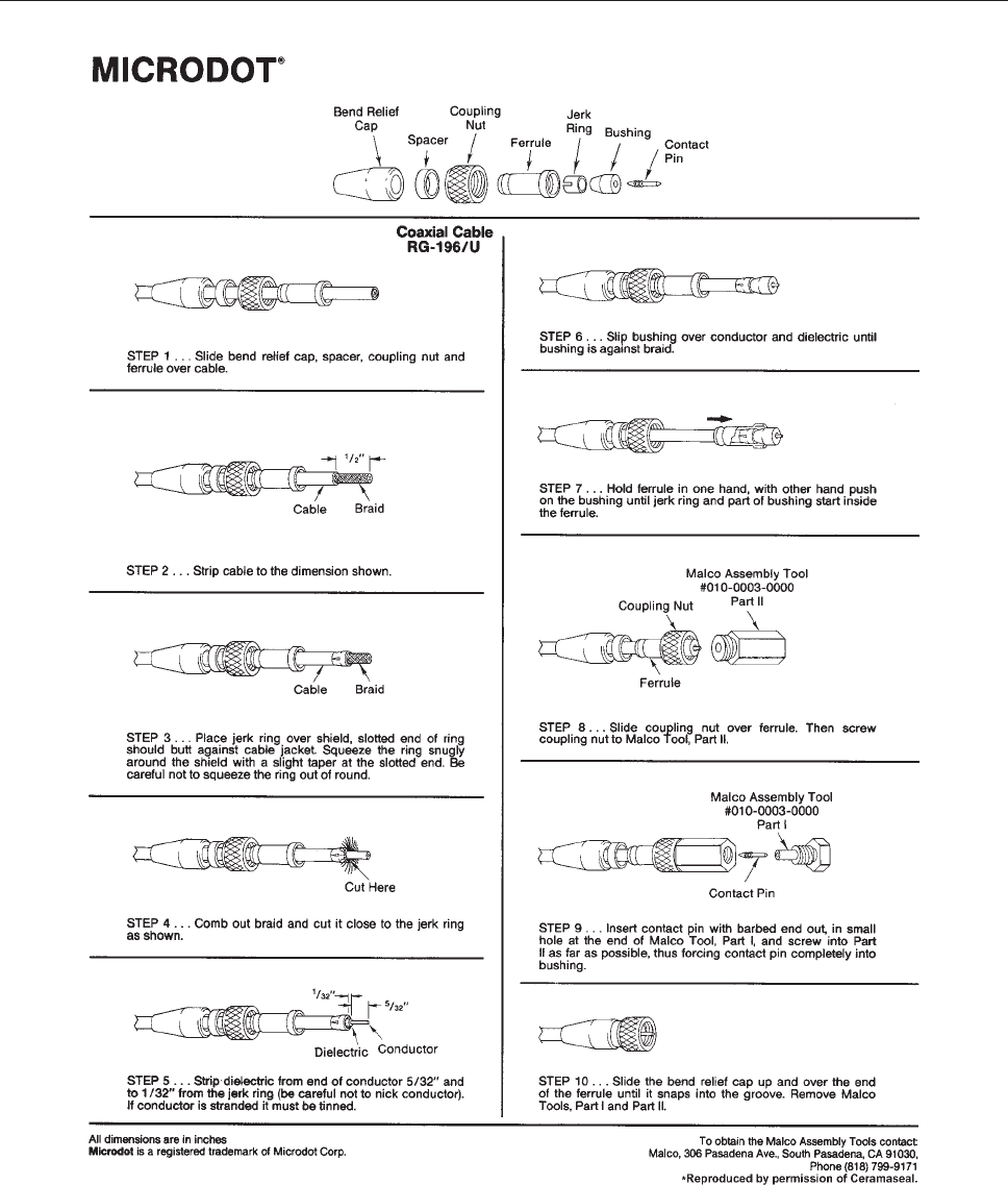
APPENDIX 541
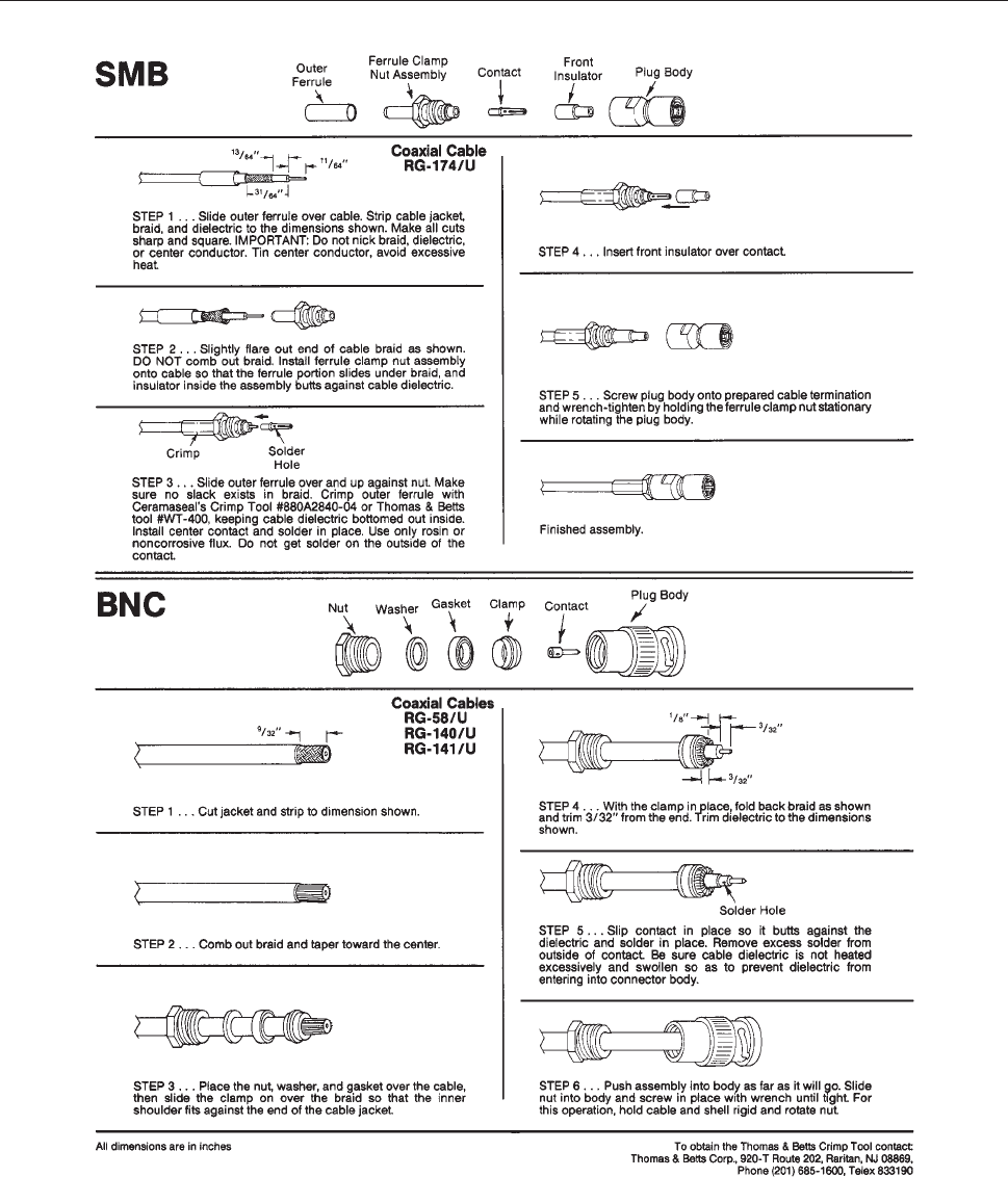
542 ELECTRONICS
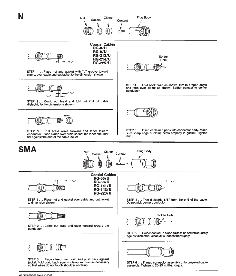
APPENDIX 543
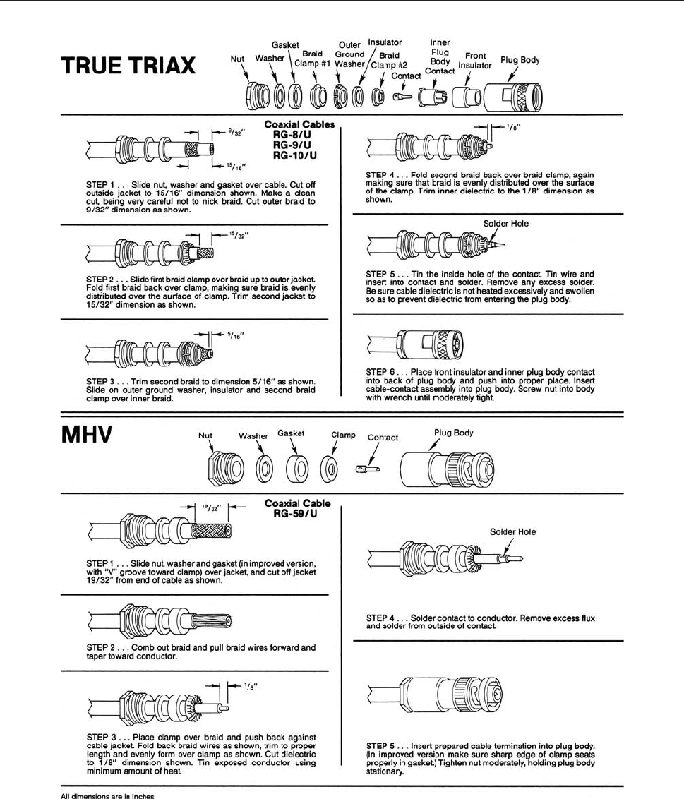
544 ELECTRONICS
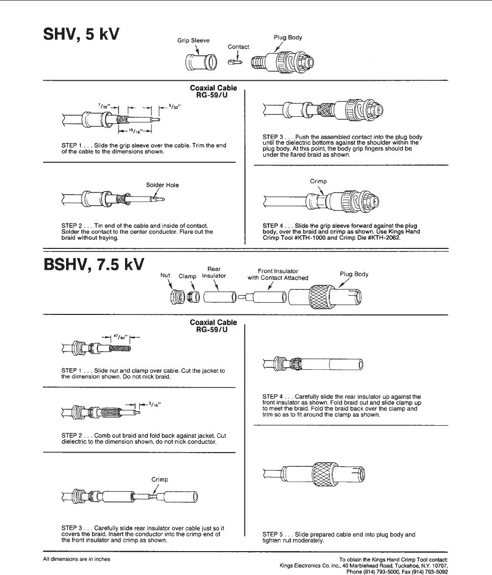
APPENDIX 545
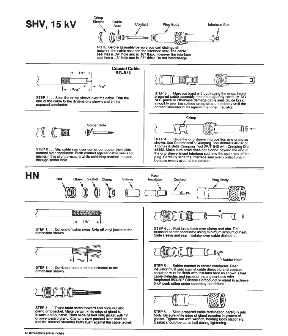
546 ELECTRONICS

DETECTORS
Phenomena that are studied experimentally often manifest
themselves as sources of electromagnetic radiation or par-
ticles. To be useful, the radiation or particles that are
involved in the experiment must be detected. In this chap-
ter we will consider the operating characteristics, selection
criteria, and performance of various types of radiation
and particle detectors. We will focus primarily on detectors
of optical radiation, from X-rays to far infrared, and on
charged-particle detectors. For a discussion of detectors
of high-energy photons, such as c rays, and elementary
particles, such as neutrons, neutrinos, and the many
particles involved in high-energy nuclear physics, we
refer the reader to the more specialized treatises on these
subjects.
1–4
7.1 OPTICAL DETECTORS
Optical detectors of various kinds detect electromagnetic
radiation from the X-ray to the far-infrared region of the
electromagnetic spectrum. In common with other branches
of electronics, the development of optical detectors has
occurred by a series of advances through the use of gas-
filled tubes and vacuum tubes to various semiconductor
devices. Gas-filled and vacuum-tube devices still retain
some niche electronics applications, such as high-voltage
switching, microwave power amplification, and special-
ized audio. Gas-filled photodetectors, which offer some
degree of signal amplification in low-cost consumer ap-
plications, have essentially disappeared. Vacuum-tube
photodetectors, especially photomultiplier tubes, remain in
wide-spread use for detection of radiation below about 1 lm.
This is especially true for low-light-level signal detection
(photon counting), and in applications where a large detector
area is required (as in scintillation counters). The designer
of an optical system is confronted with a broad range of
detector types: vacuum-tube, semiconductor, and thermal.
The last category includes thermopiles, pyroelectric detec-
tors, Golay cells, and bolometers, each with its own advan-
tages and disadvantages.
The choice of detector for a given application will
almost invariably involve a choice from among the numer-
ous commercially available devices in each of these cate-
gories. The construction of optical detectors is rarely
undertaken in the laboratory except by the specialist. The
choice of detector will be governed by factors such as:
(1) The wavelength region of the radiation to be detected
(2) The intensity of the radiation to be detected
(3) The time response required to resolve high-speed
events
(4) The detector surface area required
(5) The environmental conditions in which the detector is
to be used
(6) The cost
(7) The electronics to be used in conjunction with the
detector.
The choice of a detector for a particular experiment
should not be an exercise performed in isolation. The other
components of the experimental system may influence it,
and vice versa. This is particularly true if very weak radi-
ation is to be detected. In such a situation, action should be
taken to maximize the light signal actually reaching the
detector; this will involve a careful choice of optical com-
ponents to be placed between source and detector – for
547
CHAPTER
7

example, suitable light collection and focusing optics. If
the light from the source must pass through a dispersing
element (monochromator, etalon, etc.) before reaching the
detector, then the choices of dispersing element and detec-
tor are likely to be interrelated. Some dispersing elements
have high resolution (see Section 4.7), but low light
throughput;
others the reverse. Still others have high
throughput and resolution, but can only be scanned in a
restricted way, if at all. In a given experimental situa-
tion, the various requirements of resolution, light through-
put, scanability, and available detector sensitivities must
be offset one against another in arriving at a sensible
compromise.
Detectors can be classified as photon detectors or ther-
mal detectors. In photon detectors, individual incident
photons interact with electrons within the detector mate-
rial. This leads to detectors based on photoemission, where
the absorption of a photon frees an electron from a mate-
rial; photoconductivity, where absorption of photons
increases the number of charge carriers in a material or
changes their mobility; the photovoltaic effect, where
absorption of a photon leads to the generation of a potential
difference across a junction between two materials; the
photon-drag effect, where absorbed photons transfer their
momentum to free carriers in a heavily doped semiconduc-
tor; and photochemical detectors, such as the photographic
plate.
In thermal detectors, the absorption of photons leads to
a temperature change of the detector material, which may
be manifest as a change in resistance of the material, as in
the bolometer; the development of a potential difference
across a junction between two different conductors, as in
the thermopile; or a change of internal dipole moment
polarizability in a temperature-sensitive ferroelectric crys-
tal, as in a pyroelectric detector. With the exception of the
last, thermal detectors have slow time response when com-
pared to photon detectors. They do, however, respond uni-
formly at all wavelengths (in principle).
Photon detectors can be further classified by the spectral
region to which they are sensitive. Most photoemissive
detectors operate from the soft X-ray region through
to about 1.2 lm and rapidly become insensitive beyond
1 lm. New semiconductor photocathodes, however, are
becoming available that are sensitive out to 1.7 lm. Photo-
diodes operated in a ‘‘Geiger’’ mode provide single photon
detection capability from about 250 nm to 1.8 lm. Photo-
conductive and photovoltaic detectors based on different
materials are used right from the visible into the very far
infrared, at least to 1000 lm. Photographic films, which
are also photon detectors, generally respond best in the
visible, although films marginally sensitive out to about
1.2 lm are available. Films with appropriate fluorescent
coatings respond, to ultraviolet light.
This brief survey is not intended to be exhaustive. Many
other detection mechanisms have been described, but not
all are commonly used or are commercially available. For
more information and details about detectors in general
than will be found here, the reader should consult Refer-
ences 5–16, and the catalogs of manufacturers.
7.2 NOISE IN OPTICAL DETECTION
PROCESS
The issue of noise becomes of great importance when an
optical detector is used for detection of a weak signal.
Noise is the randomly fluctuating voltage or current pro-
duced by the detector and its associated electronics, which
interferes with the ability of the system to see the signal
being looked for. There are several sources of noise, and an
understanding of their origin and magnitude is very impor-
tant in designing a detection system that has the ability to
see the desired signal. A noise voltage or current fluctuates
both positively and negatively about zero on a timescale
that is determined by the frequency response of the system
generating the noise. Consequently, if the noise is charac-
terized by a current i
N
, the aver age noise current is <i
N
> ¼ 0.
The noise must therefore be characterized by its mean
square value, averaged over a suffi cien tly long time <i
2
N
>.
This is often called the noise power, although strictly
speaking, the noise power is <i
2
N
>R, where R is an effective
resistance through which the noise current flows. There are
several important sources of noise, which deserve separate
consideration.
7.2.1 Shot Noise
Shot noise, also called photon noise,orquantum noise,is
inescapable. This is noise associated with the signal being
548 DETECTORS

detected. If a light signal being detected gives an average
detected current of < i
S
>, then the shot noise is:
<i
2
N
>
SN
¼ 2e<i
S
>Df ð7:1Þ
where e is the magnitude of the electronic charge, and Df is
the frequency bandwidth being detected. Filtering the out-
put signal and reducing the operating bandwidth will
reduce this noise. Shot noise arises because of the discrete
nature of the charge carriers produced in the detection
process. A given detected current examined microscopi-
cally reveals itself to be a sequence of current impulses,
which, although arriving at an average rate over time, fluc-
tuate in a random way. The individual current impulses
have a characteristic time duration, determined by the time
response of the detector. If each current impulse was in-
finitely narrow – as d function – then the frequency spec-
trum of the noise would be flat or white over all
frequencies. In reality, the shot noise spectrum is flat over
frequencies up to a maximum value determined by the
time response of the detector. If the detector has a time
constant s, determined by resistance and capacitance, then
its 10% to 90% rise time is t
r
¼ 2.197s. The bandwidth Df
is related to s by:
Df ¼
1
2ps
ð7:2Þ
7.2.2 Johnson Noise
Johnson noise, also called thermal noise or Nyquist noise,
is associated with the effective resistance of the detector
circuit. For a resistance R it is described by a noise power:
<i
2
N
>
JN
¼
4kTDf
R
ð7:3Þ
where k is Boltzmann’s constant, and T is the absolute
temperature. Johnson noise arises because of the black-
body radiation associated with an enclosure at absolute
temperature T. A resistor at temperature T acts as an an-
tenna for the electric fields of the local blackbody radia-
tion. If the resistor did not reradiate its detected fields, then
it would not remain in thermal equilibrium. Consequently,
it generates a noise current.
7.2.3 Generation-Recombination (gr) Noise
Generation-recombination (gr) noise is most important
in lightly doped semiconductors. It results from the ran-
dom recombination of electrons and holes in the material.
The noise power for gr noise can be written as:
<i
2
N
>
gr
¼
4<i
2
>s
Nð1 þ 4p
2
Df
2
Þ
ð7:4Þ
where s is the characteristic time constant for recombina-
tion in the semiconductor, and
N is the average number of
carriers.
7.2.4 1/f Noise
1/f noise, also called flicker noise, current noise or excess
noise, is still not well understood. It contributes at low
frequencies, and has been shown to continue to increase
down to frequencies as low as 10
–4
Hz. 1/f noise power can
be written as:
<i
2
N
>
1=f
¼
K< i>
a
Df
f
n
ð7:5Þ
where K is a constant for a particular device, <i> is the
average (d.c.) current through the device, a lies between
0.5 and 2, and n ;1. Because 1/f noise dominates at low
frequencies, measurements at very low frequencies should
be avoided whenever possible. In experiments where light
emission results from some form of stimulation, for exam-
ple in fluorescence or light scattering, it is generally possi-
ble to periodically excite the phenomenon and move the
detection to a frequency synchronous with the excitation.
Good examples involve lock-in detection, boxcar averag-
ing, or digital signal averaging (see Chapter 6 for more
details).
Thermal noise and shot noise have so-called white
spectra – they contribute equal noise signals in a given
detection bandwidth at any frequency. Current noise gen-
erally shows a 1/f frequency dependence. As shown in
Figure 7.1, gr noise contributes at frequencies up to a value
of
the order of the reciprocal of the carrier lifetime, and
then falls off rapidly with increasing frequency.
NOISE IN OPTICAL DETECTION PROCESS 549
7.3 FIGURES OF MERIT FOR
DETECTORS
Before discussing individually the characteristics of com-
monly used and commercially available detectors, the vari-
ous figures of merit used by manufacturers to specify their
products will be described. These are the noise-equivalent
power (NEP), detectivity (D
*
), responsivity (R), quantum
effi cienc y (g), and time constant (s), which allo w such ques-
tions to be answered as: What is the minimum light intensity
falling on the detector that will gi v e rise to a signal voltage
equal to the noise voltage from the detector? What signal
will be obtained for unit irradiance? How does the electrical
signal from the detector vary with the wavelength of the light
falling on it? What is the modulation frequency response
of the detector or its ability to respond to short light pulses?
7.3.1 Noise-Equivalent Power
The noise-equivalent power (NEP) is the rms value of the
sinusoidally modulated radiant po wer falling upon a detector,
that giv es an rms signal voltage equal to the rms noise voltage
from the detector . The NEP is usually specifi ed in terms of a
blackbody source at 500 K, the reference bandwidth for the
detection of signal and noise (usually 1 or 5 Hz), and the
modulation frequency of the radiation (usually 90, 400, 800
or 900 Hz). For example, a noise-equiv alent power written
NEP (500 K, 900, 1) implies a blackbody source at 500 K, a
900Hz modulation frequency, and a 1 Hz detection band-
width. Thus, if a radiant intensity I (W/m
2
) falls on a detector
of sensitive area A (m
2
), and if signal and noise voltages V
S
and V
N
are measured with bandwidth Df (Hz) (small enough
so that the noise voltage frequency spectrum is flat within it),
then the NEP measured is:
NEP ¼
IA
ffiffiffiffiffiffi
Df
p
V
N
V
S
WHz
1=2
ð7:6Þ
7.3.2 Detectivity
At one time, detectivity was defined as the reciprocal of the
NEP. Most detectors exhibit an NEP that is proportional to
the square root of the detector area; so a detector-area-
independent detectivity D
*
is now used, specified by:
D
¼
ffiffiffi
A
p
NEP
ð7:7Þ
D
*
is specified in the same way as NEP: for example,
D
*
(500 K, 900, 1). To specify the variations in response
of a detector with wavelength, the spectral detectivity is
used. Thus, the symbol D
*
( k, 900, 1) would specify the
response of the detector to radiation of wavelength k,
Figure 7.1 Schematic frequency dependence of noise in semiconductor detectors; i
N
is
the noise current.
550 DETECTORS
modulated at 900 Hz and detected with a 1 Hz bandwidth.
The units of D
*
are cm Hz
1/2
W
–1
. Curves of D*(k) for
various detectors are shown in Figure 7.2.
F
or a thermal detector of absorptivity and emissivity e,
at absolute temperature T
1
, completely enclosed by an
environment at temperature T
2
, the photon-noise-limited
detectivity can be shown to be:
5
D
¼
4:0 3 10
16
e
1=2
ðT
5
1
þ T
5
2
Þ
1=2
cm Hz
1=2
W
1
ð7:8Þ
For a photon detector, the limiting spectral detecti vity is:
5
D
ðkÞ¼
c
0
gðmÞ
2hmp
1=2
ð
‘
v
0
gðm
0
Þv
0
2
h
nm
0
=kT
2
dm
0
ðe
hv
0
=kT
2
1Þ
2
"#
1=2
ð7:9Þ
where g(m) is the quantum efficiency of the photoemissive
surface (the average number of free electrons produced for
each incident photon absorbed), k ¼ c
0
/m, and m
0
is the
lowest frequency to which the detector is sensitive. Spec-
tral detectivities predicted by Equation (7.9) are descibed
by
Kruse, McGlauchlin, and McQuistan.
5
7.3.3 Responsivity
The responsivity R (A/W) of a detector specifies its
response to unit irradiance:
<¼i
s
=P ð7:10Þ
A similar figure of merit, usually used to characterize pho-
toemissive detectors, is the radiant sensitivity S, which is
the current per unit area of the photoemissive surface pro-
duced by unit irradiance:
S ¼
i
S
P
ð7:11Þ
Figure 7.2 Variation of the Detectivity (D
*
) as a function of wavelength for a comprehensive set of
different detectors.
FIGURES OF MERIT FOR DETECTORS 551
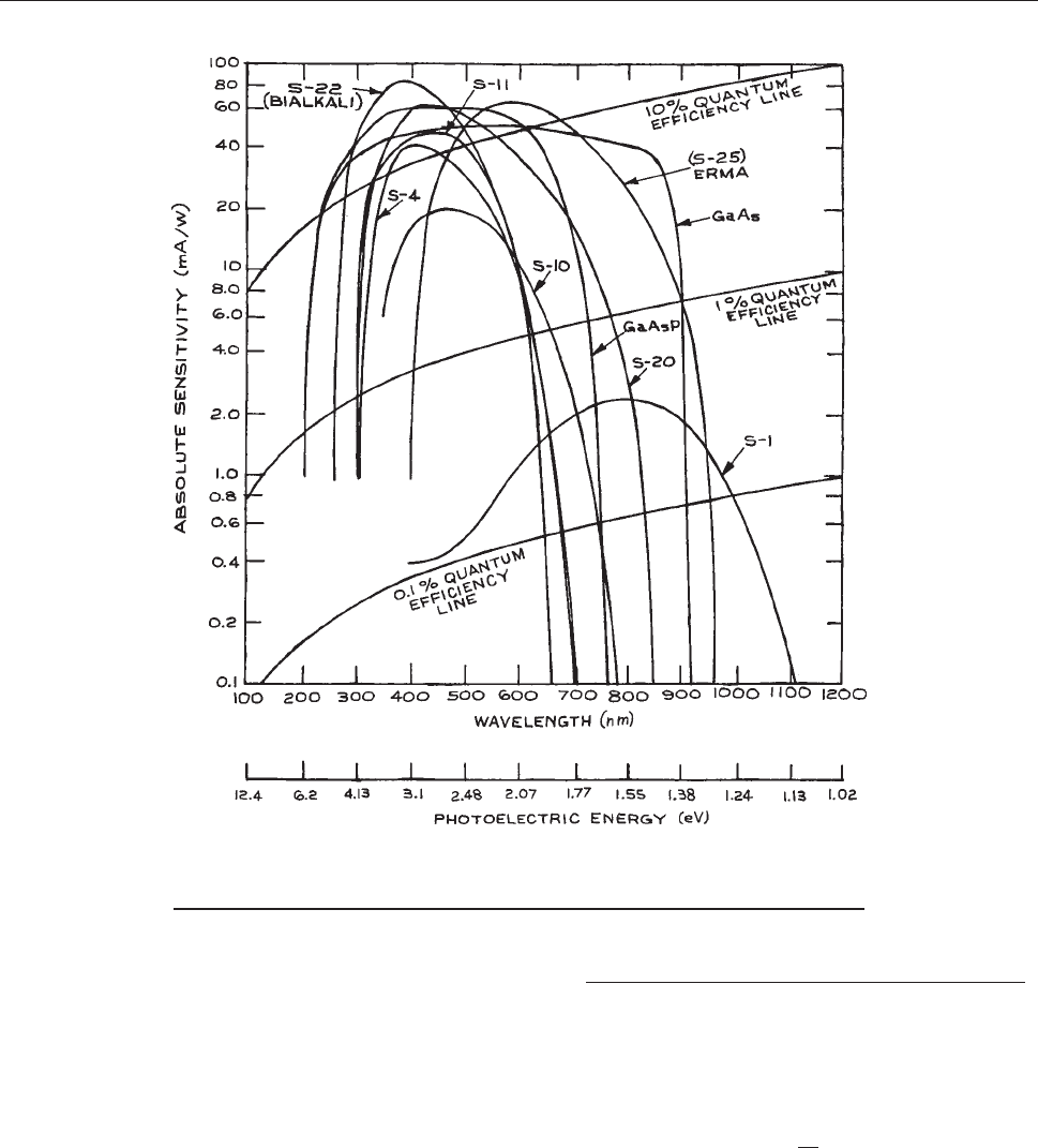
where i
S
is the total current from the detector and P the
total radiant power falling on it. Some curves showing the
spectral variation of radiant sensitivity for different photo-
emissive surfaces are given in Figure 7.3.
7.3.4 Quantum Efficiency
For a photon detector, the quantum efficiency is
de fined as:
g ¼
number of electrons or electronhole pairs produced
number of photons absorbed
ð7:12Þ
It is easy to show that the quantum efficiency of a photon
detector and its responsivity are related according to:
<¼
ge
hm
ð7:13Þ
where e is the magnitude of the electronic charge.
Figure 7.3 Wavelength dependence of the radiant sensitivity of several commercially
available photocathode materials. (From Handbook of Lasers, R. J. Pressley (Ed.), CRC
Press, Cleveland, 1971; by permission of the CRC Press.)
552 DETECTORS
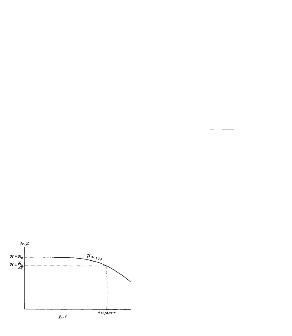
7.3.5 Frequency Response and
Time Constant
The frequency response of a detector is the variation of
responsivity or radiant sensitivity as a function of the mod-
ulation frequency of the incident radiation. The signal
from the detector should be a.c.-coupled; otherwise the
generated d.c. signal that is produced as the detector begins
to fail to respond to the modulation will also be detected.
The frequency variation of R and the time constant s of the
detector are generally related according to:
<ðf Þ¼
<ð0Þ
ð1 þ 4p
2
f
2
s
2
Þ
1=2
ð7:14Þ
like a low-passs filter, as shown in Figure 7.4.
Thus
the responsivity has decayed to a value of
<ð0Þ=
ffiffiffi
2
p
at a frequency 1/2ps. The time constant s is a
simple measure of the ability of the detector to respond
to a sharply rising or falling optical signal.
A very important parameter that determines the fre-
quency response of a detector is its capacitance. For driv-
ing a 50 ohm load, for example, a capacitance of 1 pF will
limit time constant to 50 ps. With the exception of photo-
multiplier tubes (PMTs) there is a direct relationship
between detector size and time constant. Photomultiplier
tubes with a sensitive area of 2000 mm
2
can respond as
quickly as 1–2 ns. However, for semiconductor detectors
there is no escaping the size/time-constant relationship.
For example, a semiconductor with a 1 mm sensitive area
will have a limiting time response of 1 ns and a bandwidth
of 160 MHz. On the other hand, a small size photodiode
with a diameter of 25 lm and designed for direct coupling
to optical fiber will have a bandwidth out to 20 GHz.
7.3.6 Signal-to-Noise Ratio
The random fluctuations in the output voltage or current
from a detector set a lower limit to the radiant power that
can be detected, given the detector temperature and
operating conditions, source modulation frequency, and
electronic-detection-system bandwidth. The signal-to-
noise ratio (S/N ratio) is the ratio of electrical power pro-
duced by the detected light to the noise power, which can
be written in a simple form as:
S
N
¼
<i
2
S
>
<i
2
N
>
ð7:15Þ
where i
S
is the current produced by the detected light, and
i
N
is the noise current. Angular brackets < > indicate
time averaging. Noise can often be reduced by operating
the detector in an appropriate way. In a practical detection
system, the detector must be coupled to various forms of
electronic processing systems, pre-amplifiers, amplifiers,
filters, lock-in detectors, and so on. This electronic system
necessarily creates additional noise; in a well-designed
system this is kept to a minimum.
It will be seen in the following sections that there are
various ways to reduce, and even essentially eliminate,
detector noise. Photon noise, however, which arises from
the signal itself cannot be eliminated. Thus, the ultimate
performance of any detector is photon-limited. The
photon-noise limit is different for thermal detectors, which
are sensitive to total absorbed radiation, and photon detec-
tors, which respond, at least in a microscopic way, to the
absorption of individual quanta.
The signal-to-noise (S/N) performance of a detector in a
given situation can usually be calculated from the detector
characteristics specified by the manufacture and the cha-
racteristics of the electronic system that the detector will
drive. Specifically important are the dark-noise level, the
noise figure [especially for devices with internal gain such
as avalanche photodiodes (APDs)], the quantum efficiency
(or responsivity) of the detector, and the input impedance
of the following electronics and its noise characteristics.
Figure 7.4 Typical frequency dependence of
detector responsivity R.
FIGURES OF MERIT FOR DETECTORS 553
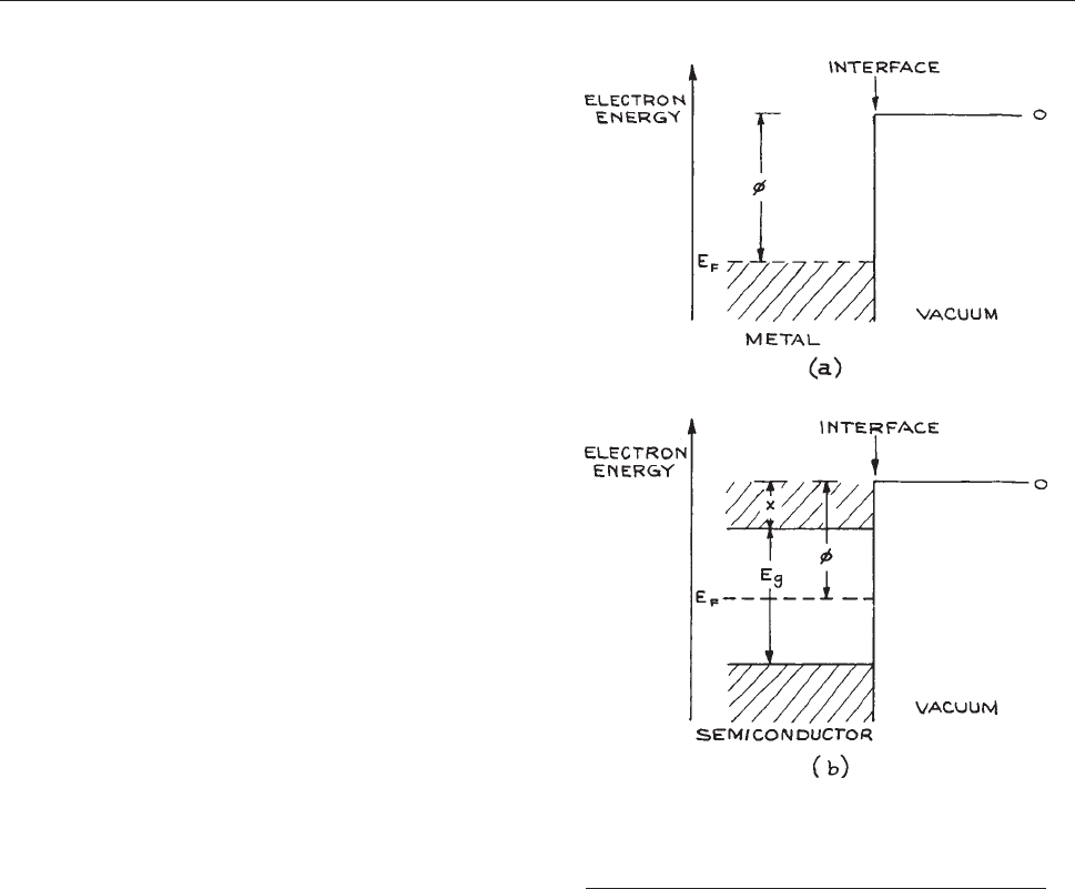
Davis
6
has provided several examples of how to calcu-
late detector noise performance in various situations.
If the detector manufacturer specifies D* or NEP, and
not all do, signal-to-noise calculations can be simplified.
Frequently the dark-noise current will be specified, usually
in units of nA or pA. Noise generally increases with the
square root of the bandwidth used. For example, a detector
with a bandwidth of 100 MHz and a dark current of 5 nA
has a dark noise of 0.5 pA/
ffiffiffiffiffiffi
Hz
p
.
7.4 PHOTOEMISSIVE DETECTORS
Photoemissive detectors include vacuum photodiodes,
photomultiplier tubes, microchannel plates, and photo-
channeltrons. These are all p hoton detectors that utilize
the photoelectric effect. When radiation of frequency m
falls upon a metal surface, e lectrons are emitted if the
photon energy hm is greater than the work function /
characteristic of the material being irradiated. A simpli-
fied energy-level diagram illustrating this effect for a
metal–vacuum interface is shown in Figure 7.5(a).Formost
m
etals, /; is in a range from 4–5 eV (1 eV [ 1.24 lm)
although for the alkali metals it is lower, for example,
2.4 eV for sodium and 1.8 eV for cesium. Pure metals,
alloys, (particularly beryllium–copper) and cesium iodide
are used as phot oemissive surfaces in ultraviolet an d
vacuum-ultraviolet detectors. Lower work functions, and
consequently sensit ivities that can be extended into the
infrared, can be obtained with special semiconductor
materials. Figure 7.5(b) shows a schematic energy-level
diag
ram of a semiconductor–vacuum interface. In this
case the work function is defined as / ¼ E
vac
– E
F
, where
E
F
is the energy of the Fermi level. In a pure semiconduc-
tor, the Fermi level is in the middle of the band gap, as
illustrated in Figure 7.5(b).Inap-ty
pe doped semiconduc-
tor, E
F
moves down toward the top of the valence band,
while in n-type material it moves up toward the bottom of
the conduction band. Consequently, /; is not so useful a
measure of the minimum photon energy for photoemission
as it is for a metal. The electron affinity v is a more useful
measure of this minimum energy for a semiconductor.
Except at absolute zero, photons with energy hv > v cause
photoemission. Photons with energy hm > E
g
lead to the
production of carriers in the conduction band: this leads to
intrinsic photoconductivity, which is the operative detec-
tion mechanism in various infrared detectors, such as InSb.
7.4.1 Vacuum Photodiodes
Once electrons are liberated from a photoemissive surface
(a photocathode), they can be accelerated to an electrode
(the anode), positively biased with respect to the cathode,
and generate a signal current. If the acceleration of photo-
electrons is directly from cathode to anode through a vac-
uum, the device is a vacuum photodiode. Because the
Figure 7.5 Band structure of: (a) a metal–vacuum
interface and (b) a pure semiconductor–vacuum
interface (/ ¼ work function; v ¼ electron affinity;
E
g
¼ band-gap energy; E
F
¼ Fermi level).
554 DETECTORS
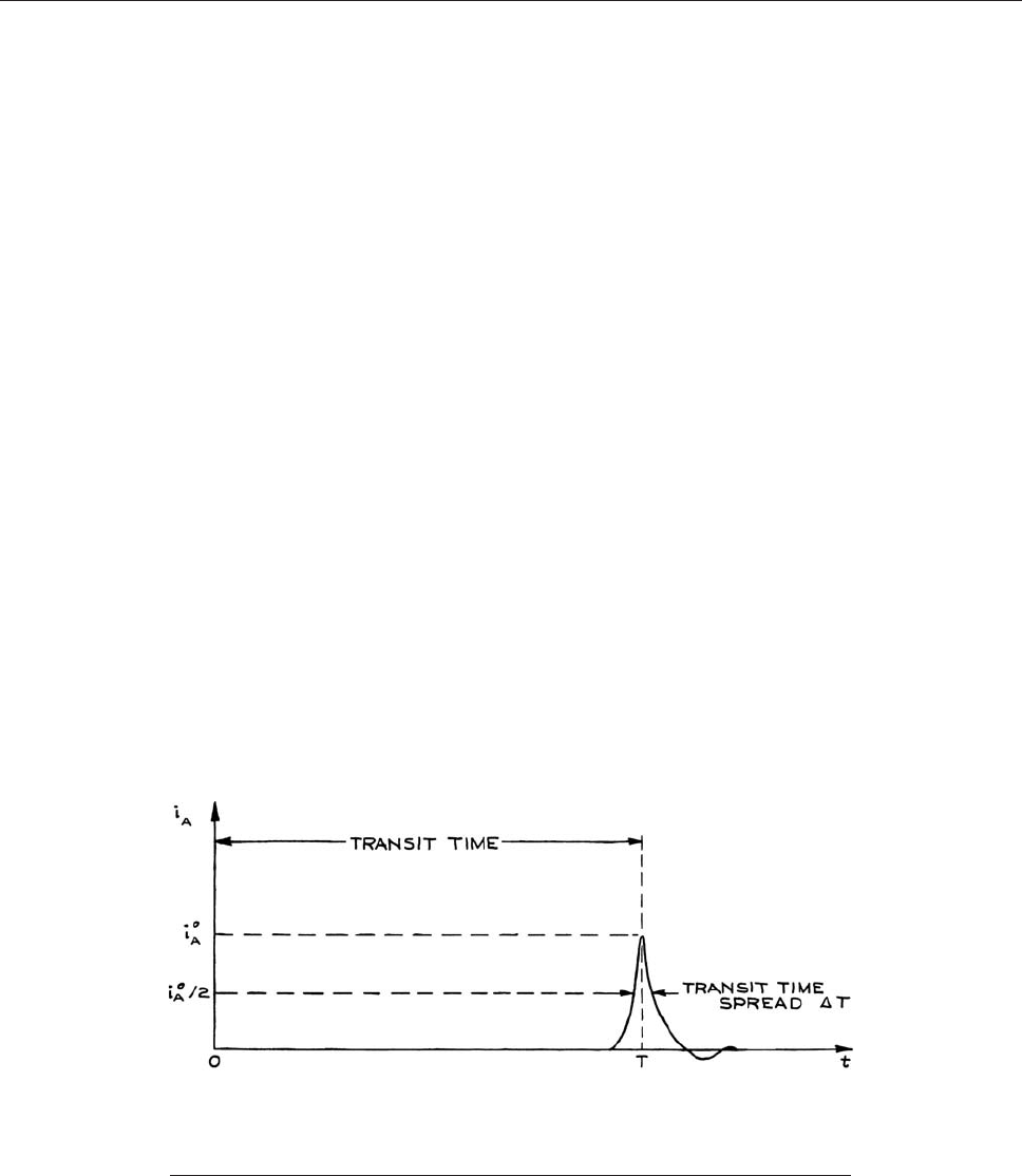
electrons in such a device take a very direct path from anode
to cathode and can be accelerated by high voltages – up to
several kilovolts in a small device – vacuum photodiodes
have the fastest response of all photoemissive detectors.
Rise times of 100 ps or less can be achieved. External con-
nections and electronics are generally the limiting factors in
obtaining short rise times from such devices. Vacuum pho-
todiodes, however, are not very sensitive, since, at most, one
electron can be obtained for each photon absorbed at the
photocathode.
If the space between photocathode and anode is filled
with a noble gas, photoelectrons will collide with gas
atoms and ionize them, yielding secondary electrons.
Thus, an electron multiplication effect occurs. However,
because the mobility of the electrons moving from cathode
to anode through the gas is slow, these devices have a long
response time, typically about 1 ms. Gas-filled photocells
are no longer competitive with solid-state detectors and
have disappeared from use.
7.4.2 Photomultipliers
If photoelectrons are accelerated in vacuo from the pho-
tocathode and allowed to strike a series of secondary
electron-emitting surfaces, called dynodes, held at progres-
sively more positive voltages, a considerable electron mul-
tiplication can be achieved and a substantial current can be
collected at the anode. Such devices are called photomul-
tipliers. Practical gains of 10
9
(anode electrons per photo-
electron) can be achieved from these devices for short light
pulses. Continuous gains must be held lower, to perhaps
10
7
. This limit is imposed primarily by the ability of the
final dynodes in the chain to withstand the thermal loading
produced by continuous electron impact, and by the time
needed for the dynodes to be recharged when large cur-
rents are drawn from the anode. Because of their very high
gain, photomultipliers can generate substantial signals
when only a single photon is detected: for example, an
anode pulse of 2 ns duration containing 10
9
secondary
photoelectrons produced from a single photoelectron will
generate a voltage pulse of 4 V across 50 ohms. This,
coupled with their low noise, makes photomultipliers very
effective single-photon detectors. Photomultiplier D
*
values
can range up to 10
16
cm Hz
1/2
W
–1
. Only the dark-adapted
human eye, which can detect bursts of about 10 photons in
the blue, comes close to this sensitivity.
The time-response characteristics of photomultiplier
tubes depend to a considerable degree on their internal
dynode arrangement. The response of a given device can
be specified in terms of the output signal at the anode that
results from a single photoelectron emission at the photo-
cathode. This is illustrated in Figure 7.6. Because electrons
passing
through the dynode structure can generally take
slightly different paths, secondary electrons arrive at the
anode at different times. The anode pulse has a character-
istic width called the transit-time spread, which usually
ranges from 0.1 to 20 ns. The time interval between
Figure 7.6 Typical anode pulse produced by a single photoelectron emission at
the cathode of a photomultiplier tube. t is the time following photoemission. The
transit-time T, the transit-time speed DT, and the peak anode current i
A
0
all fluctuate
from pulse to pulse.
PHOTOEMISSIVE DETECTORS 555

photoemission at the cathode and the appearance of an
anode pulse is called the transit time, and is usually a
few tens of nanoseconds. The transit time and transit-time
spread also fluctuate slightly from one single-photoelec-
tron-produced anode pulse to the next. Although this is a
fine point, it may be something to worry about in precision-
timing experiments. The principle suppliers of photomul-
tiplier tubes are Hamamatsu, Burle Industries
17
(now
merged with Photonis), Electron Tubes, Phillips
(Amperex), Photek, and Sens-Tek.
There are s even main types of dyn ode structure in
common usage in photomultiplier tubes; these are illus-
trated in Figure 7.7 . The circular cage stru cture [Figure
7.7
(a)] (use d, for example, in the H amamatsu 1P28 pho-
tomultiplier tube) is compact and can be designed for
good electron-collection efficiency and small transit-
time spread. This dynode structure works well with opaque
photocathodes, but is not very suitable for high-amplification
requirements, where a larger number of dynodes is re-
quired. The box-and-grid [Figure 7.7(b)] and Venetian-
blind structures [Figure 7.7(c)] (used, for example, in the
Hamamatsu Models R464 and R1513, respectively) offer
very good electron-collection efficiency. Because they col-
lect multiplied electrons independent of their path through
the dynode structure, a wide range of secondary-electron
trajectories is possible, leading to a large transit-time
spread and slow response. Typical response times of these
types of tube are 10–20 ns. Venetian-blind tubes can easily
be extended to many dynode stages and have a very stable
gain in the presence of small power-supply fluctuations.
These tubes also have an optically opaque dynode struc-
ture providing very low dark-current noise when operated
under appropriate conditions.
The focused dynode structure [Figure 7.7(d)] (used, for
example, in the Hamamatsu R331, R2059, and the old
Phillips 56 AVP and other 56-series tubes
18
) is designed
so that electrons follow paths of similar length through the
dynode structure. To accomplish this, electrons that devi-
ate too much from a specified range of trajectories are not
collected at the next dynode. These types of tube offer
short response times, typically 1–2 ns; some recently
developed tubes are even faster.
The mesh type of dynode structure [Figure 7.7(e)] has a
series of crossed fine-mesh dynodes arranged in close
proximity. The structure allows compact construction,
high immunity to magnetic fields, as well as uniformity
of response and good pulse linearity. Versions of this type
with special anodes provide position-sensitive perform-
ance. In this type of device the output signal from a series
of anodes provides direct information on the location of
illumination on the photocathode surface.
The metal-channel dynode structure [Figure 7.7(g)] pro-
vides a very compact dynode structure and fast response
becomes of the closeness between each stage of dynodes.
This structure also allows position-sensitive detection.
Good examples of this type of tube are in the Hamamatsu
R5900 series. These types of tube can tolerate quite large
magnetic fields. The Hamamatsu R5946 tube has been
shown to operate satisfactorily in fields of 4kG.
19
Closely rela ted to thes e f unda men tal photomult iplier
dynode structures is the micro channel plate (MCP) [Fig-
ure 7.7(f)]. Instead o f traditional dynodes, photoelectrons
enter a bundle of capillary tubes fused together in an
array. Each tube has a resistive coating on its inner sur-
face that acts as a continuo us electron multiplier. Each
capillary individually can be referred to as a channel
electron multiplier (CEM) [or channeltron (a trademark
of Burle Industries)]. In these capillaries electrons make
multiple reflections from the tube walls generating sec-
ondary electrons. MCPs have fast time response, good
immunity from external magnetic fields, and position-
sensitive capability when provided with multiple anodes.
These devices are available commercially from Burle
(Photonis), DelM ar Ventures, El-M ul, Hamamatsu, Pho-
tek, TecTra, and Topag. CEMs a re primarily used for
particle detection (see later).
Other types of multiplier structures, not shown in Figure
7.7, are also available. Traveling-wave phototubes and var-
ious
types of crossed-field photomultiplier have very short
response times, down to 0.1 ns.
20
7.4.3 Photocathode and Dynode Materials
The performance of a photomultiplier depends not only
on its internal structure, but also on the photoemissi v e mate-
rial of its photocathode and the secondary-electron-emitting
material of its dynodes. The selection of a photodiode or
photomultiplier for a particular spectral response depends
on an appropriate selection of photocathode material. The
wavelength dependence of various commercially available
556 DETECTORS
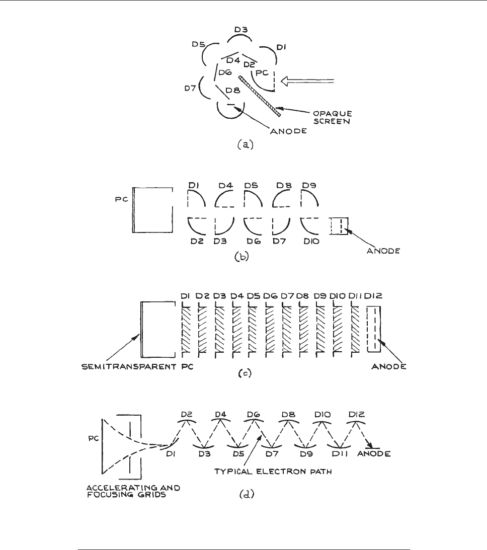
Figure 7.7 Schematic diagram of the internal structure of various types of
photomultiplier tube; (a) circular cage; (b) box and grid; (c) Venetian blind;
(d) focused dynode; (e) mesh type; (f) microchannel electron multiplier;
(g) metal-channel dynode structure. D ¼ dynode; PC ¼ photocathode.
PHOTOEMISSIVE DETECTORS 557
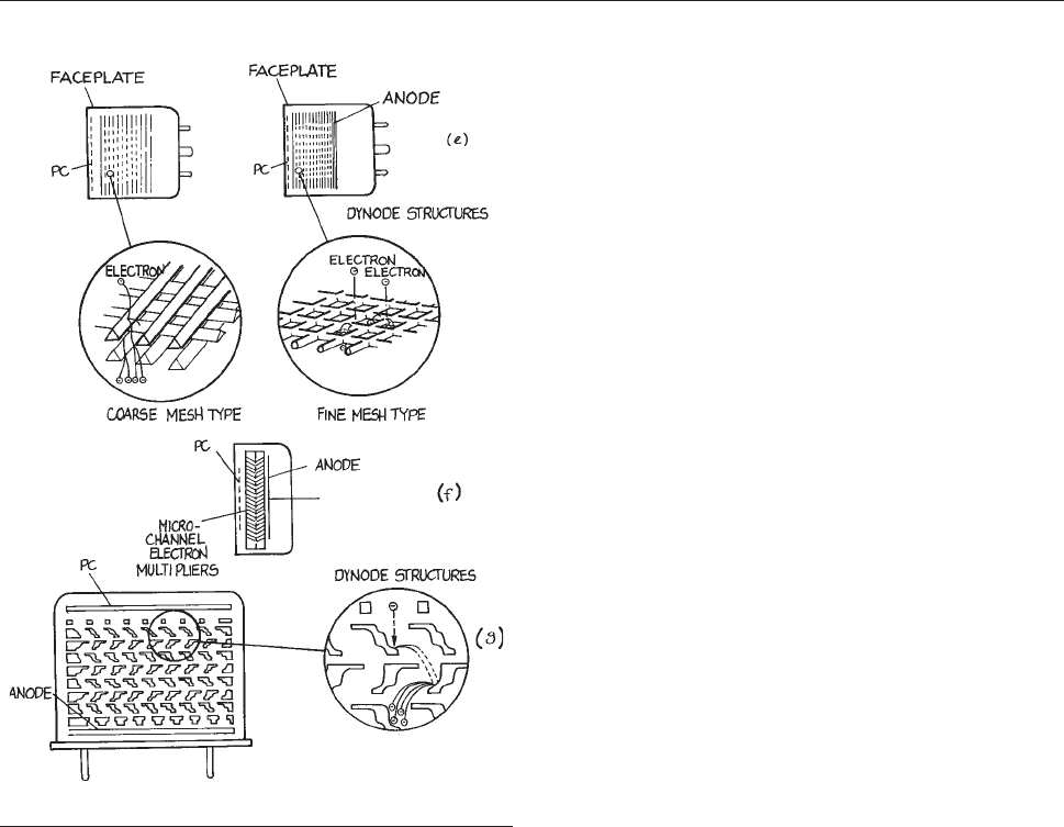
photocathode materials is shown in Figure 7.3;someradiant
sensitiviti es and quantum ef fi ciencies are giv en in Table 7.1.
Figure 7.8 sho ws the radiant sensiti vities and quantum effi-
cien
cies of some new negative electron af fi nity (NEA) pho-
tocathode materials. Practical quantum efficiencies for
photoemissiv e materials range up to about 0.4. The short-
wavelength cutoff of a given material depends on its work
function. This cutoff is not sharp because, except at absolute
zero, there are always a few electrons high up in the con-
duction band available for photoexcitation by low-energy
photons. Some few of these electrons, because of their ther-
mal excitation, will be emitted without any photostimulation.
This contributes the major part of the dark current observed
from the photocathode. Materials that have low work func-
tions, and are consequently more red- and infrared-sensitiv e,
have higher – often much higher – dark currents than mate-
rials that are optimized for visible and ultraviolet sensiti vity.
Such photocathodes are best operated cooled. Unless a pho-
totube is to be used primarily for detecting long-wavelength
radiation, we recommend selecting a photocathode with the
shortest possible wav elength response.
Photocathodes are available in both opaque and semitrans-
parent forms, depending on the model of phototube. In the
semitransparent form the photoelectrons are ejected from the
thin photoemissiv e layer on the side opposite to the incident
light. In both types the photocathode has to perform two
important functions: it must absorb incident photons and
allow the emitted photoelectrons to escape. The latter ev ent
is inhibited if photons are absorbed too deep in a thick photo-
emissi ve layer , or if the photoelectrons suffer energy loss from
scattering in the layer . If the emitted photoelectron has too
much energy, it can excite a further electron across the band
gap. This pair-production phenomenon inhibits the release of
photoelectrons from the photoemissive layer, and accounts for
the ultraviolet cutoff characteristics of the different materials
show n in Figure 7.3. W ith reference to Figure 7.5(b), it can be
sh
own that for pair production to occur , the incident photon
energy must be greate r than 2E
g
. For materials where v < E
g
,
photoelectrons have their best chance of escaping, and the
photocathode its highest quantum efficienc y.
Because semitransparent photocathodes allow photons
to penetrate sufficiently for photoelectrons to escape on the
far side of the layer, they are deposited as semiconductor
layers on the insulating glass substrate of the entrance
window. These photocathodes are less tolerant of relatively
high light levels than are opaque photocathodes, which can
be deposited on a conductive substrate. A conductive sub-
strate preserves field distribution within the PMT even at
relatively large cathode currents. When an opaque photo-
cathode is used, photons pass through the entrance window
of the PMT and strike the photocathode, which is mounted
separately, as shown schematically in Figure 7.7(a). Photo-
electrons
are emitted on the same side of the photocathode
as photons are absorbed.
Practical photoemissive materials fall into two main
categories: classical photoemitters and NEA materials.
Classical photoemitters generally involve an alkali metal
or metals, a group V element, such as phosphorus, arsenic,
Figure 7.7 (cont.)
558 DETECTORS

antimony, or bismuth, and sometimes silver and/or oxygen.
Examples are the Ag-O-Cs (S1) photoemitter, which has
the highest quantum efficiency beyond about 800 nm of
any classical photoemitter, and Na
2
KSbCs, the so-called
tri-alkali (S-20) cathode.
Negative electron affinity photoemitters have only been
developed within the last 15 years. These materials gen-
erally utilize a photoconductiv e single-crystal semiconductor
substrate, with a very thin surface coating of cesium and
usually a small amount of oxygen. The cesium (oxide)
layer lowers the electron affinity below the value it would
have in the pure semiconductor, achieving an effectively
negative value. Examples of such NEA photoemitters are
GaAs (CsO) and InP (CsO). Negative electron affinity
emitters can offer very high quantum efficiency and
extended infrared response. For example, GaAs (CsO)
has higher quantum efficiency in the near infrared then an
S-1 photocathode. Other new NEA photocathodes include
InP/InGaAsP (sensitive to 1.4 lm) and InP/InGaAs (sensi-
tive to 1.7 lm). Commercial photomultipliers with NEA
photocathodes are available from Burle Industries and
Hamamatsu, that offer response out to 1.7 lminatube
cooled to 100 °C. Development of NEA photoemitters is
continuing
21
, and the experimentalist seeking long-
wavelength response would be well advised to follow the
literature and check for the introduction of new commercial
tubes. For further details about NEA materials, the inter-
ested reader should consult the article by Zwicker.
22
Table 7.1 Characteristics of photoemissive surfaces
Cathode Radiant Sensitivity (mA/W) 1.06 lm Peak Quantum
Efficiency (%)
kpeak
(lm) Cathode Dark
Current
a
(A/cm
2
)
515 nm 694 nm
S-1 Cs-O-Ag 0.6 2 0.4 0.08 800 9 3 1
–12
S-10 Cs-O-Ag-Bi
b
20 2.7 0 5 470 4 3 10
16
Cs
3
Sb on MnO
c
39 0.2 0 13 440 10
16
(tri-alkali) 53 20 0 18 470 9 3 10
16
S-22 (bi-alkali) 42 0 0 26 390 2 3 10
15
GaAs
d–g
48 28 0 14 560
h
10
16
GaAsP
d
60 30 0 19 400 3 3 10
15
InGaAs(Cs)
d,f
7 2.6 0.1 15 380 2 3 10
14
InP/InGaAs
d,e,f
3 3 11(1.5 lm) 1.55 lm
h
4 3 10
14
InP/InGaAsP
d,f
3 3 10(1.3 lm) 1.3 lm
i
4 3 10
15
S-25 (ERMA)
j
53 26 0 25 430 1 3 10
15
Cs-Te (solar blind) — — — 15 254 2.5 3 10
17
Note: Table shows typical values, but these can vary greatly from one manufacturer to another. We recommend that manufacturers’ data
sheets be consulted for more details.
a
At room temperature.
b
Cathode designated S-3 is similar.
c
Several types of CsSb photocathodes exist where the CsSb is deposited on different opaque and semitransparent substrates and various
window materials are used.These photocathodes have the designations S-4, 5, 13, 17, and 19 as well as S-11.
d
NEA photoemitters.
e
Available from Burle Industries.
f
Available from Hamamatsu Corporation.
g
Available from Hamamatsu Corporation.
h
Sensitive out to 1.7 lm. Exact spectral characteristics will depend on thickness of photoemitter and whether it is used in transmission
or not.
i
Sensitive out to 1.4 lm. Exact spectral characteristics will depend on thickness of photoemitter and whether it is used in transmission
or not.
j
Extended-red S-20.
PHOTOEMISSIVE DETECTORS 559
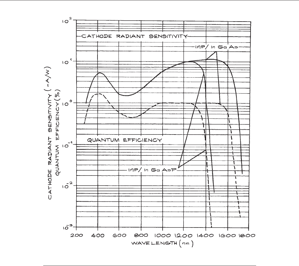
The performance of the dynode material in photomulti-
plier tubes is specified in terms of the secondary-emission
ratio d, as a function of energy. For a phototube with n
dynodes the gain is d
n
. In the past, the most common
dynode materials were CsSb, AgMgO, and BeCuO. The
last is also used as the primary photoemitter in windowless
photomultipliers that are operated in vacuo for the
detection of vacuum-ultraviolet radiation. BeCuO can be
reactivated after exposure to air. The above materials
have d-values of 3–4. Newer NEA dynode materials have
much higher d-values; in particular, that of GaP can range
up to 40 for an incident-electron energy of 800 eV. With
such high d-values, a photomultiplier tube needs fewer
dynodes for a given gain, but with larger interdynode
accelerating voltages. Such tubes are compact and provide
fast time response. In very many commercial photo
multipliers, at least the first dynode is now often made
of GaP. This offers improved characterization of the single-
Figure 7.8 Quantum efficiencies and radiant sensitivities of near-infrared semiconductor
photocathode materials.
560 DETECTORS
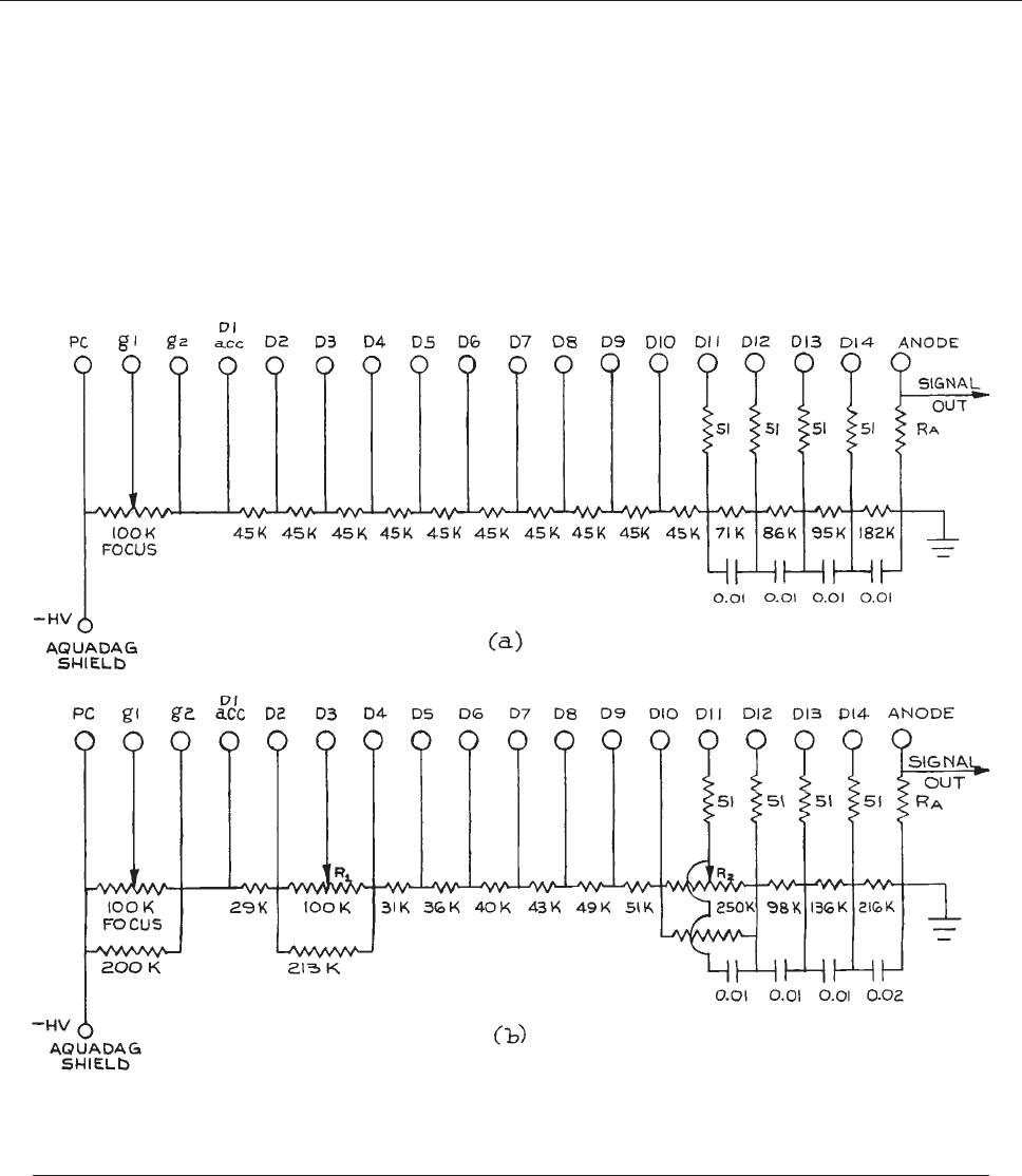
photo-electron response of the tube, which is important in
designing a system for optimum signal-to-noise ratio.
7.4.4 Practical Operating Considerations
for Photomultiplier Tubes
Complete photomultiplier assemblies are available, in
which the tube, mounting base, dynode chain and output
connector are pre-packaged. Suppliers include C&L
Instruments, Hamamatsu, OE Technologies, and Products
for Research, For the experimentalist who desires more
control over tube operation, the following sections should
be useful. (Note also that Hamamatsu have published a
comprehensive guide to photomultiplier use.
23
)
Dynode Chains. The accelerating voltages are supplied
to the dynodes of a photomultiplier by a resistive voltage
div ider called a dynode chain. The relative resistance v alues
Figure 7.9 Dynode chains for Phillips 56-series photomultiplier tubes: (a) chain for high gain and fast time response;
(b) chain for high linearity (R
1
and R
2
adjusted for optimum performance). PC ¼ photocathode; g1,g2 ¼ grids;
acc ¼ accelerator grid; D1–D14 ¼ dynodes. Resistance values are in ohms, capacitance values in lF. For very low-level
light detection, all resistances can be scaled upward to reduce overall chain current.
PHOTOEMISSIVE DETECTORS 561
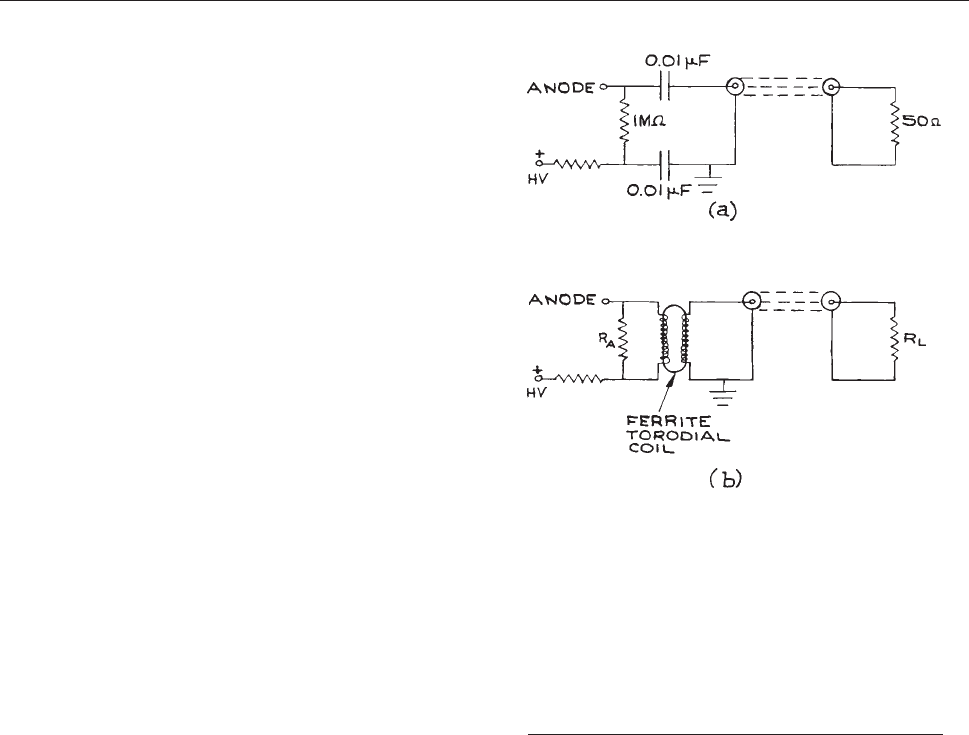
in the chain determine the distribution of voltages applied to
the dynodes. The total chain resistance R determines the
chain current at a given total photocathode–anode applied
voltage. Some phototubes are supplied with an integral
dynode chain, but most are not. Adequate dynode-chain
designs are generally supplied by the manufacturer with
each tube. Alternative designs intended for certain types of
response, such as maximum gain for short pulses or highest
linearity, can frequently be found by consulting the literature.
Two examples of such dynode-chain designs for use with
Phillips 56-series tubes are giv en in Figure 7.9. The total
dyn
ode-chain resistance is chosen so that the chain current
is at least 100 times greater than the average d.c. anode
current to be drawn from the tube. This current is specified
for each tube and may range as high as 1 mA for high-gain
tubes. The operation of photomultiplier tubes at such high
average currents for very long is not recommended. Long-
term d.c. anode currents should be kept between 1 and 10 lA
for most tubes.
There are several interesting features of the dynode
chains shown in Figure 7.9. The photocathode is generally
operated
at negative potential with the anode near ground.
This makes it easy to couple the output signal to other
electronics. The tube can be operated with the cathode
grounded, but in this case the signal from the anode, which
is now at high positive potential, must be coupled through
high-voltage capacitors or an insulated transformer, as
shown in Figure 7.10. The photocathode is also often con-
nected
to a conducting shield, which is either a painted
coat of colloidal graphite (Aquadag) on the outside of
the tube envelope, or a metal foil wrapped around the tube
envelope. If the photocathode is at negative potential,
appropriate insulation must be used around the tube if
the tube is in close proximity to any grounded metal parts
inside its housing.
Many photomultiplier tubes have one or more focusing
electrodes between the photocathode and the first dynode.
The voltage on these electrodes can be adjusted to opti-
mize the collection of photoelectrons from the photoca-
thode. The last three or four dynodes are decoupled with
high-voltage, high-frequency capacitors (disk ceramics
work well in this application). These capacitors prevent
depression of the dynode-chain voltage on the last few
dynodes when a large pulse of electrons passes through
the tube (the secondary-electron current drawn from each
dynode must be supplied by the dynode chain). For high-
frequency applications the inclusion of small damping
resistors (typically between 50 X and 1 kX) between the
decoupling capacitors and the dynodes is recommended. The
resistor R
A
, the anode resistor, determines the actual voltage
that will be produced by a given anode current, since the
photomultiplier serves as a current source. R
A
should not
be so large that the voltage dev eloped across it is signific ant
compared with the voltage between the anode and the last
dynode. A value of R
A
between 1 and 10 MX is usual. In
high-frequency applications, such as single-photon count-
ing, the signal from R
A
should be coupled out through a
50 X coaxial cable terminated in 50 X. In many cases, the
effective value of the anode load is set by the input impe-
dance of the electronics to which the tube is connected. In
Figure 7.10 Anode signal coupling methods for a
photomultiplier operated with the anode at high
positive potential: (a) capacitor coupling for fast-risetime,
short-pulse operation (the component sizes are typical;
the capacitors should be high-frequency, high-voltage
types); (b) transformer coupling for lower-frequency,
modulated operation (the high-voltage winding on the
transformer should be sufficiently well insulated for
isolation from the core; the size of R
A
will depend on
various factors, such as transformer primary impedance
and operating frequency).
562 DETECTORS
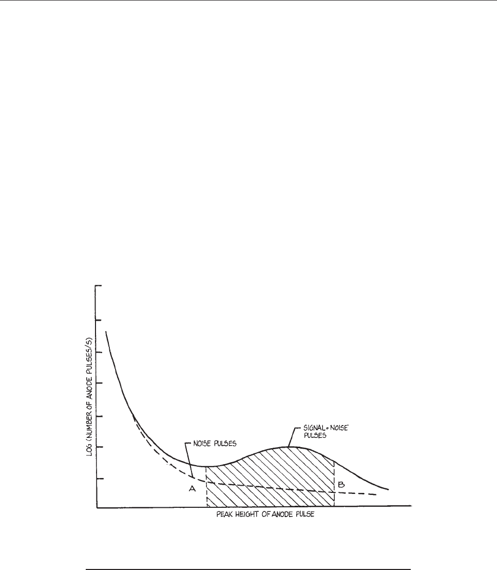
such applications the cable connection to the anode should
be shielded as close to the anode as possible, even going so
far as to insert R
A
under the grounded screen of the coaxial
cable. Some high-frequency tubes are supplied with an
integral coaxial connector on the anode. In any case, the
aim is to reduce parasitic inductance and capacitance asso-
ciated with the anode connection. For example, even with a
50 X load, a parasitic capacitance greater than 20 pF will
limit the response time of the tube to 1 ns.
The actual response-time behavior of the photomultiplier
can be determined by observing its single-photo-electron
response. This is done by looking at the anode pulses with
a fast oscilloscope, which generally requires that the 50 X
coaxial cable from the anode be terminated in 50 X.The
photocathode should not need to be illuminated for this to
be done; sufficient noise pulses will usually be observed.
The pulses should appear as in Figure 7.6. If they have
to
o much of an exponential tail they are probably
limited by the anode resistor and parasitic capacitance.
These anode pulses reflect the time distribution and number
of secondary electrons reaching the anode following single
(or multiple) photoelectron emissions from the photoca-
thode. If the height distribution of anode pulses is measured,
a distribution such as is shown in Figure 7.11 will probably
be
seen.
Mounting Photomultiplier Tubes. Photomultiplier
tubes are generally mounted by clamping their plastic
socket inside a cylindrical tube housing. The housing
should be light-tight: a photomultiplier should never be
exposed to ambient lighting when its high-voltage dynode
chain is on, for the resultant large secondary-electron
current will disintegrate the last dynodes and may strip
the photocathode layer itself. If the total power
dissipation of the dynode chain is low, the whole dynode
chain may be mounted directly on the tube socket. If space
is not at a premium, the dynode chain can be remote from
the tube base and connected to it with high-voltage-
insulated wire. The damping resistors, decoupling cap-
acitors, and anode resistor should, however, be kept in
Figure 7.11 Schematic photomultiplier anode pulse-height distribution likely to
be observed in practice. The best signal-to-noise ratio would be obtained in a
photon-counting experiment by collecting only anode pulses in a height range
roughly indicated by the shaded region AB.
PHOTOEMISSIVE DETECTORS 563

close proximity to the tube. The photomultiplier should be
mounted so there is no optical path from its base to its
photocathode.
Photomultipliers are fragile and should be mounted so
they are not subject to stress. This is particularly important
if a tube is to be cooled. In practice, this means that the
tube should be grasped at only one point in its mount.
Rugged (and expensive) photomultipliers that can with-
stand severe vibrations and accelerations are available
from ADIT and Hamamatsu.
Noise in Photomultiplier Tubes. Noise in photo-
multipliers comes from several sources:
(1) Thermionic emission from the photocathode
(2) Thermionic emission from dynodes
(3) Field emission from dynodes (and photocathode) at
high interdynode voltages
(4) Radioactive materials in the tube envelope (for example,
40
K in glass)
(5) Electrons striking the tube envelope and causing
fluorescence
(6) Electrons striking the dynodes and causing fluorescence
(7) Electrons colliding with residual atoms of vapor in the
tube (cesium for example) and causing fluorescence
(8) Cosmic rays.
Noise from photomultipliers is always greater after
they have been exposed to light (without high voltage
applied). They gradually become quieter after operation
under dark conditions for an extended period.
Noise from thermionic emission can be reduced consid-
erably by cooling the tube (particularly for S-1 tubes).
A factor of 10–1000 reduction in noise can be obtained
by cooling to about 20 °C. S-1 tubes need to be cooled
to low temperatures, but temperatures below about 70 °C
are not recommended. Too much cooling has a marginal
effect on reducing thermionic emission – which will
already be negligible for most tubes at 20 °C – and may
have deleterious effects. At low temperatures, the conduc-
tivity of the photocathode layer falls, which causes it to no
longer be an equipotential. The resultant distorted field
distribution between cathode and dynodes will increase
the possibility of noise from sources such as item (5) above.
Two convenient designs of photomultiplier-tube coolers are
shown in Figure 7.12. In the design shown in Figure
7.1
2(a), a copper or aluminum cylinder encloses the tube
(wi
thout touching it). This tube is in thermal contact with a
chamber containing Dry Ice (or liquid nitrogen). Conden-
sation on the face of the photomultiplier tube is minimized,
since moisture preferentially condenses and freezes on the
much colder metal tube. In the second design, shown in
Figure 7.12(b), cold nitrogen gas boiled off from a liquid-
ni
trogen Dewar flows through a copper tube surrounding
the photomultiplier, and finally sprays over its photoca-
thode surface to minimize water-vapor condensation. The
rate of supply of cold nitrogen gas can be adjusted to pro-
vide a range of temperatures.
Photomultiplier-tube coolers are available from Amherst
Scientific, Electron Tubes, Hamamatsu, and Products for
Research.
When noise from field emission is a problem with cer-
tain high-voltage, high-gain tubes, one solution is to
reduce the voltage. In single-photon-counting experi-
ments, larger than normal anode pulses may result from
field emission and can be rejected with an appropriate
window discriminator.
24
Noise from radioactive envelope materials should gen-
erally be negligible. Noise from electrons striking the tube
envelope can be reduced by a shield around the tube held
at photocathode potential. Noise from electrons striking
the dynodes and causing fluorescence causes the fewest
problems in Venetian-blind tubes, which have little or no
direct optical path from dynodes to photocathode. Noise
from gas in the tube can be a problem in old tubes, which
frequently become gassy; solution: buy a new tube. Noise
from cosmic rays is usually unimportant; it can be reduced
by shielding.
Of all these sources of noise, thermionic emission
from the photocathode is generally by far the most impor-
tant. For a given photocathode material the total noise
will depend on the photocathode area. Most manufac-
turers will list the dark current observed at the anode.
The values in Table 7.1 have been derived from man-
ufacturers’
anode dark currents corrected for tube gain
and photocathode area. Under comparable conditions,
tubes with a small photocathode area, like the old S-20
ITT FW-130 with a photocathode diameter of 0.25 cm,
are less noisy than tubes with large photocathodes, like
the 46 mm photocathode of the S-20 Hamamatsu R550.
In many experiments a large photocathode area is
564 DETECTORS
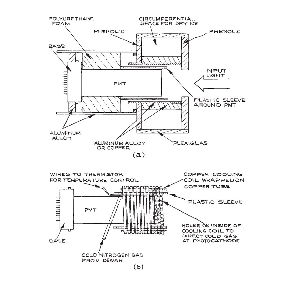
unnecessary – light coming through a monochromator slit
illuminates a very small area. The effective photocathode
area, and consequently its thermionic noise, can be reduced
by wrapping a magnetic coil around the photocathode,
which prevents electrons other than those from the center
of the photocathode from reaching the first dynode. Under
circumstances where photomultipliers must be operated
in close proximity to magnetic fields, magnetic shields to
Figure 7.12 Photomultiplier-tube coolers: (a) using Dry Ice reservoir in thermal contact
with a metal tube close to, but electrically insulated from, the photocathode; (b) using
cold nitr ogen gas cir culated around tube and sprayed onto photocathode surface
(a thermistor monitors temperature and allows control of the rate of supply of cold gas).
PHOTOEMISSIVE DETECTORS 565
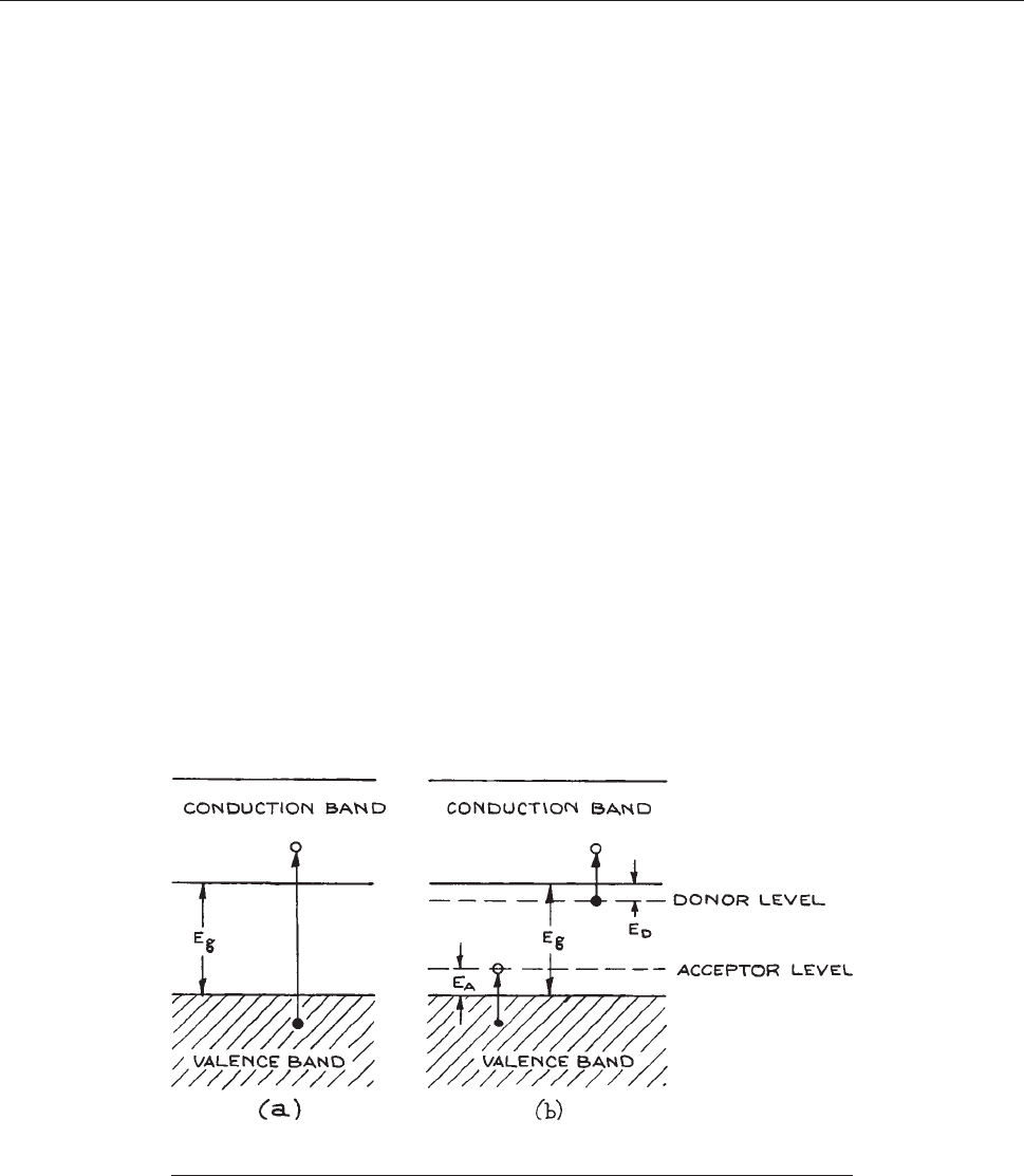
enclose the tube are available from Ad-Vance Magnetics,
Amuneal, Magnetic Shield Corp. (Perfection Mica), Mu
Shield, and Products for Research.
In the anode pulse-height distributions shown in Figure
7.11, small anode pulses are much more likely to corre-
spond
to noise than are pulses in the middle of the distri-
bution. In photon-counting experiments these small pulses
should be rejected with a discriminator. Awindow discrim-
inator provides simultaneous rejection of these pulses and
those which are much larger than average.
25
Ultraviolet and Vacuum-Ultraviolet Detection
with Photodiodes and Photomultipliers.
For
detection of radiation down to about 105 nm, phototubes
with windows of LiF are available, as are tubes with
windows of MgF
2
or sapphire. Windowless phototubes or
CEMs are used for detection of even shorter wavelengths.
For detection of radiation down to 58 nm or beyond,
conventional photomultiplier tubes sensitive to visible
light (S-11) can be used if the outer surface is coated with
a layer of sodium salicylate – or if a sodium-salicylate-
coated disk is placed close to the photocathode. Sodium
salicylate fluoresces in the visible with almost
unity quantum effi ciency and converts incident vacuum-
ultraviolet radiation to a wavelength where a conv entional
tube can detect it. The response of the sodium salicylate is
also fast, so that 1 ns ultraviolet detection is possible. To
prepare a sodium-salicylate-coated windo w, a solution of
sodium salicylate in reagent-grade methanol (80 g/L) is
atomized and sprayed onto the windo w, at a distance of
about 10 cm from the atomizer. Commercial nasal sprays
and air brushes pressurized with dry nitrogen are suitable
for this purpose. The atomizer should be far enough from
the windo w that no large drops can be deposited. The
method works better if the window is kept warm (50–
70 °C). Spraying should be continued until the density of
the sodium salicylate layer reaches about 20 g/m
2
,which
can be determined by weighing.
7.5 PHOTOCONDUCTIVE
DETECTORS
Photoconductive detectors can operate through either
intrinsic or extrinsic photoconductivity. The physics of
intrinsic photoconductivity is illustrated in Figure 7.13(a).
Photons
with energy hm > E
g
excite electrons across the
band gap. The electron–hole pair that is thereby created for
each absorbed photon leads to an increase in conductivity
(mostly from the electrons.) Semiconductors with small
band gaps respond to long-wavelength infrared radiation
but must be cooled accordingly; otherwise thermally
Figure 7.13 Mechanism for: (a) intrinsic photoconductivity; (b) extrinsic
photoconductivity.
566 DETECTORS

excited electrons swamp any small photoconductivity
effects. Table 7.2 lists commonly available intrinsic photo-
conducti
ve detectors together with their usual operating
temperature and the limit of their long-wavelength
response k
0
, together with some representative figures for
detectivities and time constants. Note that silicon and ger-
manium are also operated in both photovoltaic and ava-
lanche modes (see Section 7.6).
If
a semiconductor is doped with an appropriate mate-
rial, impurity levels are produced between the valence and
conduction bands, as shown in Figure 7.13(b). Impurity
le
vels that are able to accept an electron excited from the
conduction band are called acceptor levels,whereas
impurity levels that can have an electron excited from
them into the conduction band are called donor levels.
Thus, in Figure 7.13(b) photons with energy hm > E
A
excite
an electron to the impurity level, leaving a hole in the
valence band and thereby giving rise to p-type extrinsic
photoconductivity. Photons with energy hm > E
D
will excite
an electron into the conduction band, giving n-type extrin-
sic photoconductivity. For example, gold-doped germa-
nium has an acceptor level 0.15 eV above the valence
band and is an extrinsic p-type photoconductor, as is cop-
per-doped germanium, which has an acceptor level 0.041
eV above the valence band. These used to be the two most
commonly used extrinsic photoconductive detectors,
responding out to about 9 lm and 30 lm, respectively,
but they have been largely superseded by mercury cad-
mium telluride (MCT) detectors. Curves showing the var-
iation of their D
*
with wavelength are given in Figure 7.14.
Table 7.3 lists the operating characteristics of some extrin-
sic
photoconductive detectors. Detectors listed with oper-
ating temperatures below 28 K will in practice frequently
be operated at 4 K, since liquid helium is a safe, available
coolant, although its use involves more complicated tech-
nology than the use of liquid nitrogen. Only long wave-
length response gallium-doped germanium detectors are
currently commercially available, although other extrinsic
Table 7.2 Intrinsic photoconductive detectors
Semiconductor T (K) E
g
(eV) k
0
(lm) D
*
(max) s
(cm Hz
1/2
W
1
)
CdS 295 2.4 0.52 3.5 3 10
14
’50 ms
CdSe 295 1.8 0.69 2.1 3 10
11
’10 ms
Si
e
295
a
1.12 1.1 <2 3 10
12
—
b
Ge
e
295
a
0.67 1.8 10
11
10 ns
c
PbS 295 0.42 2.5 <2 3 20
11
—
d
195 0.35 3.0 <5 3 10
11
—
d
77 0.32 3.3 <8 3 10
11
—
d
PbSe 295 0.25 4.2 1 < 10
9
–53 10
9
1 ls
195 0.23 5.4 1.5–4 310
10
3050 ls
77 0.21 5.8 <3 3 10
10
50 ls
InSb
e
77 ’0.23 5.5–7.0 <3 3 10
10
0.11 ls
Hg
x
Cd
y
Te
f
77 <0.1 1225 10
9
10
11
>1 ns
a
Increased sensitivity can be obtained by cooling.
b
Detectors with time constants from 50 ps upward and various detectivities are available.
c
Detectors operated in a photovoltaic mode with time constants from 120 ps upward and various detectivities are available.
d
Detectors with time constants ranging from about 100 ls to 10 ms and varying detectivities are available.
e
More commonly operated in a photovoltaic mode.
f
Wavelength range depends on stoichiometry
Silicon detectors are available from many suppliers.
26
Ge detectors are available from Jobin Yvon and Judson. PbS and PbSe detectors
are available from Cal Sensors, Hamamatsu, Judson and New England Photoconductor, InSb detectors are available from Hamamatsu,
InfraRed Associates, Judson, and Kolmar Technologies. MCT detectors are available from Boston Electronics, Hamamatsu, InfraRed
Associates, Judson, and Kolmar Technologies.
PHOTOCONDUCTIVE DETECTORS 567
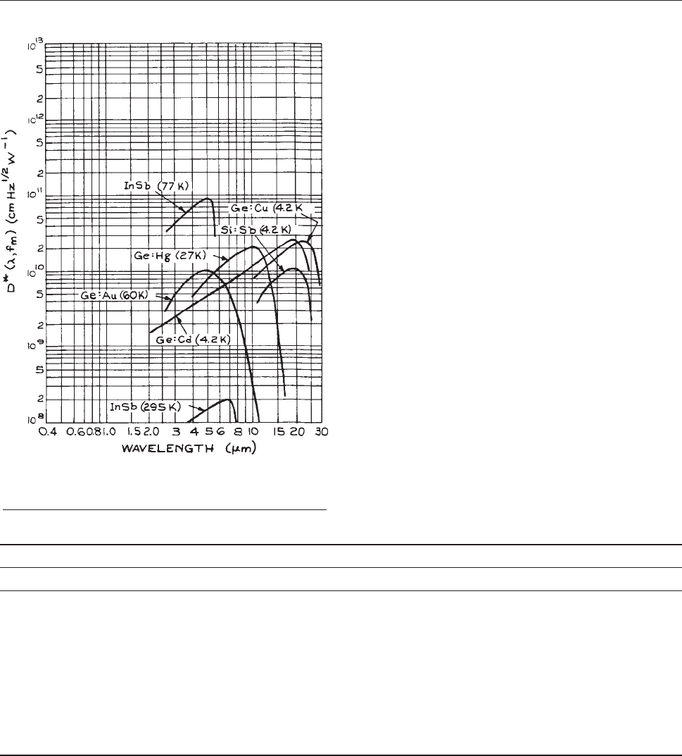
detectors are still custom made in specialized research
laboratories.
All photoconductive detectors, whether intrinsic or extrin-
sic, are operated in essentially the same way, although there
are wide differences in packaging geometry. These differ-
ences arise from dif fering operating temperatures and speed-
of-response considerations. A schematic diagram showing
the main construction features of a liquid-nitrogen-cooled
photoconductive or photovoltaic detector is giv en in
Figure 7.15. Uncooled detectors can be of much simpler
cons
truction – for example, in a transistor or flat solar-cell
package.
One feature of the cooled detector design shown in Figure
7.15 is worthy of note. The field of view of the detector is
generally
restricted by an aperture, which is kept at the
temperature of the detection element. This shields the
detector from ambient infrared radiation, which peaks at
9.6 lm. For detection of low-level narrow-band infrared
radiation the influence of background radiation can be
further reduced by incorporating a cooled narrow-band
filter in front of the detector element. The filter will only
radiate beyond the cutoff wavelength of the detector, and
thus restricts transmitted ambient radiation to a narrow
band. Liquid-helium-cooled detectors generally have a
double Dewar; an outer one for liquid nitrogen surrounds
the inner, for liquid helium. Liquid-nitrogen-cooled detec-
tors, such as HgCdTe, are recommended in preference to
liquid-helium-cooled detectors, such as Ge:Cu, whenever
Figure 7.14 D
*
(k) as a function of wavelength for various
photoconductive detectors. (Courtesy of Hughes Aircraft
Company.)
Table 7.3 Extrinsic photoconductive detectors
Semiconductor Impurity T (K) k (lm) D
*
(or NEP) s
Ge:Au
a
p-type 77 8.3 3 3 10
9
10
10
30 ns
Ge:Hg
a
p-type <28 14 1–2 3 10
10
> 0.3 ns
Ge:Cd p-type <21 21 2–3 3 10
10
10 ns
Ge:Cu
a
p-type <15 30 1–3 3 10
10
>0.4 ns
Ge:Zn
a,b
p-type <12 38 12 3 10
10
10 ns
Ge:Be p-type <3 115 2 3 10
10
>1 ls
Ge:In p-type 4 111 — <1 ls
Ge:Ga p-type 4 >200 8 3 10
13
(NEP) <1 ls
Si:Ga p-type 4 17 109–10
10
>1 ls
Si:As n-type <20 23 1–3.5 310
10
0.1 ls
a
Sometimes also contain silicon.
b
Sometimes also contain antimony.
568 DETECTORS
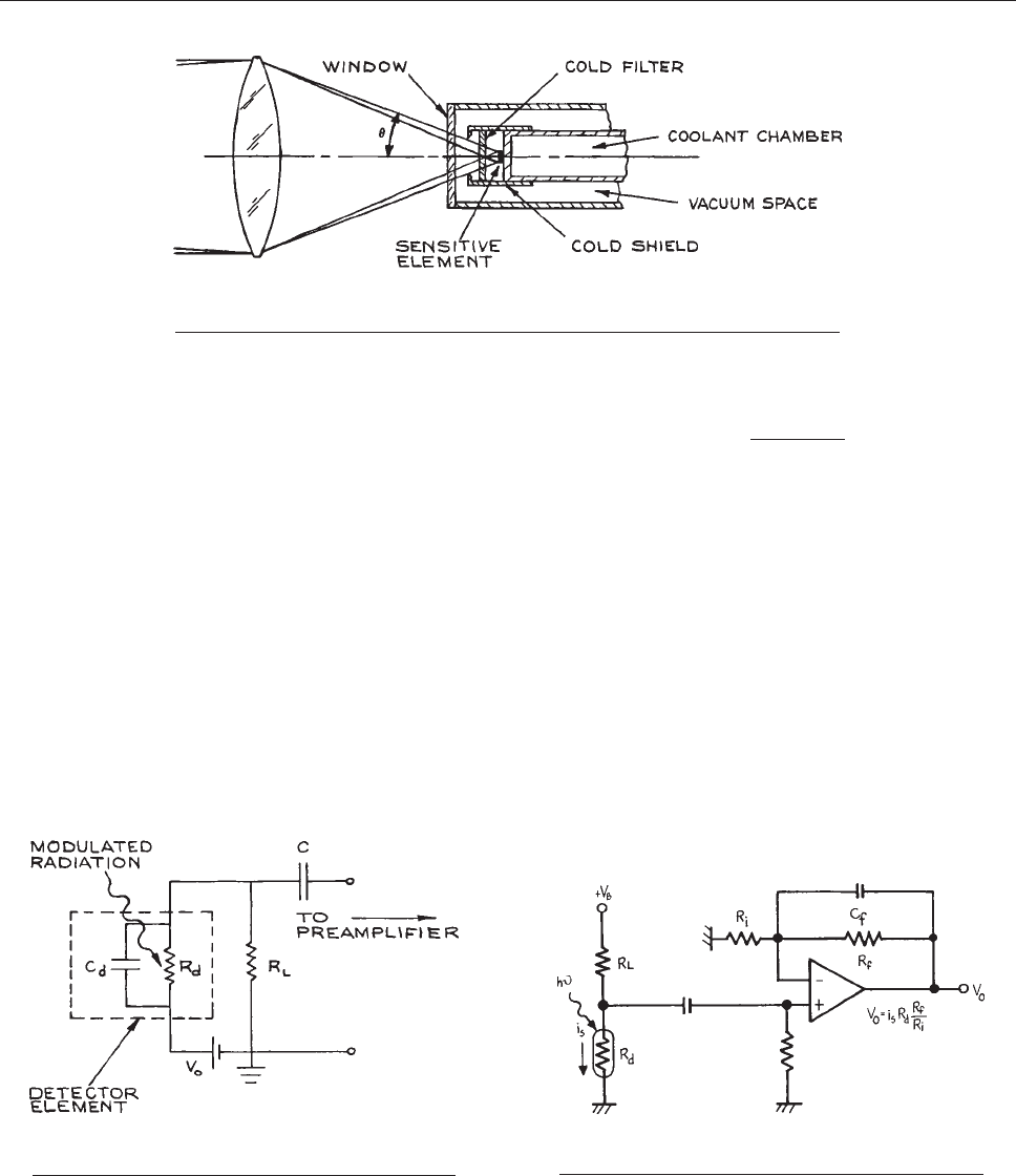
there is a choice. Some miniature-package commercial
detectors can be cooled with Joule–Thompson refrigeration
units driven with compressed gas, which eliminates the
need for externally supplied liquified-gas coolant. Thermo-
electrically cooled (Peltier effect) infrared detector pack-
ages are available from Cal Sensors, Hamamatsu, Marlow,
and New England Photoconductor, for the operation of
MCT, PbS, or PbSe detectors down to temperatures of
193 K. Further details of the operating principles behind
these and other refrigeration techniques used with infrared
detectors are given by Hudson and Hudson.
7
Figure 7.16 shows a basic biasing circuit commonly
used for operating photoconductive detectors. R
d
is the
detector dark resistance. It is easy to see that the change
in voltage, DV, that appears across the load resistor R
L
for a
small change DR in the resistance of the detector is:
DV ¼
V
0
R
L
DR
ðR
d
þ R
L
Þ
2
ð7:16Þ
This is at a maximum when R
L
¼ R
d
. Thus it is common
practice to bias the detector with a load resistance equal to
the detector’s dark resistance. The bias voltage is selected
to give a bias current through the detector that gives
optimum detectivity. This bias current will generally be
specified by the manufacturer. Figure 7.17 shows a simple
op-amp
circuit for use with a photoconductive detector.
To obtain a fast response from a photoconductive
detector, great care must be taken to minimize the stray
capacitance C
s
in the input circuit to the preamplifier.
Otherwise, the time constant of the detector will be
limited by R
L
C
S
. The ultimate limits to the speed of an
actual detector are set by its internal capacitance C
d
and
Figure 7.15 Radiation-shielded liquid-nitrogen-cooled photoconductive or
photovoltaic infrared detector assembly.
Figure 7.16 Simple biasing circuit for operating a
photoconductive detector with modulated radiation.
Figure 7.17 Simple op-amp circuit for operating a
photoconductive detector.
PHOTOCONDUCTIVE DETECTORS 569
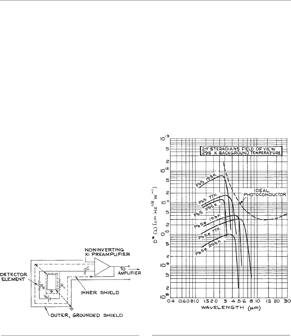
the majority-carrier lifetime. Many comme rcial detectors
are manufactured so that the stray capacitance of the
detector and its connection leads is very small. This
is generally true of high-speed commercial detectors
packaged in all-metal Dewars with integral coaxial bias
connections. Metal Dewar packages are preferable to
glass ones: although the latter are cheaper, they are very
fragile.
If a detector is not specifically packaged to minimi ze
stray inductance, it is possible to reduce the stray capaci-
tance of the detector package and improve its speed of
response by the technique of ‘‘bootstrap ping,’’ which is
illustrated in Figure 7.18. All bias leads to the detector
an
d the leads to the preamplifier are double-shielded.
The preamplifier should ideally have a high input impe-
dance, a low input capacitance, a wide bandwidth, and
50 ohm output imp edance. Such p reamplifiers can be
constructed, or bought from detector suppliers or Perry
Amplifier. The inner shield is not grounded, but is con-
nected directly to the low-impedance output of the unit-
gain preamplifier. Thus the inner shield is ‘‘bootstrap-
ped’’ to the signal voltage and stray capacitance is effec-
tively eliminated. By this means the speed of response of
a detector can be improved substantially, say from 1 ls
down to 50 ns. An alternative way to improve the speed
of response, at the expense of signal (but not detectivity),
is to reduce the value of the load resistor.
A few photoconductive detectors are worthy of brief extra
comment. Silicon and germanium are much more commonly
used for photodiodes, frequently in an avalanche mode. These
devices are discussed in Section 7.6. Lead sulfide detectors
ha
ve high impedance, 0.5 to 100 MX, and slow response, but
are the most sensitive detectors in the spectral region between
2and3lm and can be used uncooled. D
*
(k) curves for
these detectors are shown in Figure 7.19. They are available
from
Cal Sensors, Hamamatsu, Judson, and New England
Photoconductor. Lead selenide is sensitive to longer wave-
lengths than lead sulfide, but InAs operated in a photovoltaic
mode is to be preferred in this spectral region (3–4 lm).
InSb operated in a photov oltaic mode is probably the detector
of choice between 4 and 5.3 lm. Beyond about 5 lm,
HgCdTe (MCT) is the detector of choice and is to be pre-
ferred to detectors such as Ge:Hg and Ge:Cu, which must be
operated below liquid-nitrogen temperature. MCT detectors
Figure 7.18 Arrangement for ‘‘bootstrapping’’ an infrared
detector to minimize effects of parasitic capacitance.
Figure 7.19 D
*
as a function of wavelength for various
lead-salt photoconductive detectors. (Courtesy of Hughes
Aircraft Company.)
570 DETECTORS
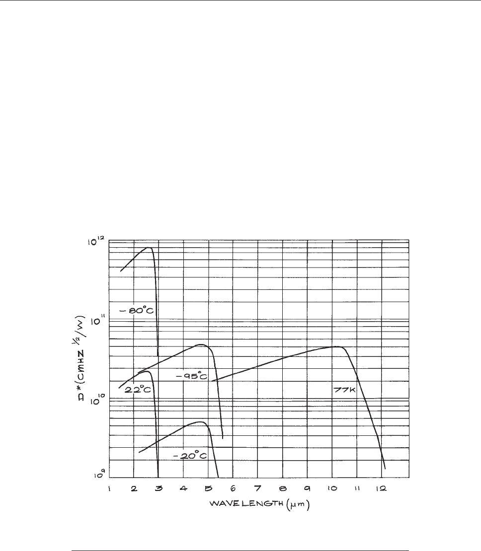
can be operated in either a photoconductive or photov oltaic
mode. HgCdTe comes in different stochiometries, generally
represented as Hg
x
Cd
1–x
Te. Different stoichiometries have
diff erent spectral responses. By varying its composition,
HgCdTe exceeds in performance all other 77 K detectors
between 6 and 12 lm. Sometimes these detectors also
contain zinc and are designated HgCdZnTe. Thermoelec-
trically cooled MCT detectors have higher detectivity at
shorter wavelengths than MCT detectors operated at
77 K, as s hown in Figure 7. 20. HgCdTe detectors are
avai
lable from Boston Electronics, Hamamatsu, InfraRed
Associates, Judson, and Kolmar Technologies. For fur-
ther details of the above detectors, t he reader should con-
sult References 5, 7, 12, and 26 . Supplie rs of other
detectors
are listed in Reference 25.
The
use of extrinsic photoconductivity for the detec-
tion of far-infrared radiation requires the introduction of
appropriate dopi ng materi al into a semiconduc tor in order
to generate an acceptor or donor impurity level extremely
close to the valence or conduction bands, respectively.
Well-characterized impurity levels have been generated
in germanium in this way using gallium,
27
indium,
28
boron,
29
or beryllium doping. The long-wavelength sensi-
tivity limit is restricted to about 120 lm, but can be
extended to 200 lm in Ge:Ga by stressing the crystal.
Ge:Ga detectors are available from QMC Instruments.
Longer-wavelength-sensitive, extrinsic photoconductivity
can be observed in appropriately doped InSb in a magnetic
field. Bulk InSb can be used more efficiently for infrared
detection in a different photoconductive mode entirely.
30
Figure 7.20 D
*
as a function of wavelength for room temperature, thermoelectrically
cooled, and liquid nitrogen cooled (77 K) mercury cadmium telluride photovoltaic
detectors manufactured by Judson.
PHOTOCONDUCTIVE DETECTORS 571
Even at the low temperature at which far-infrared photo-
conductive detectors operate (< 4 K), there are carriers in
the conduction band. These free electrons can absorb far-
infrared radiation efficiently and move into higher-energy
states within the conduction band. This change in energy
results in a change of mobility of these free electrons,
which can be detected as a change in conductivity, using
a circuit such as the one shown previously in Figure 7.17.
Som
e typical wavelength response curves are shown in
Figure 7.21. These hot
-carrier-effect photoconductive
detectors or hot-electron bolomoters can be used success-
fully over a wavelength range extending from 50 to 10
4
lm;
they have detectivities up to about 1 3 10
11
cm Hz
1/2
W
–1
and response times down to 1 ls. They are frequently oper-
ated in a large magnetic field (several hundred kA/m or
more). These detectors are av ailable from QMC Instruments.
Magnetically tuned detectors are also available from QMC
Instruments. These detectors are tuned in wavelength
response by operating them in a magnetic field.
31,32
7.6 PHOTOVOLTAIC DETECTORS
(PHOTODIODES)
In a photovoltaic detector photoexcitation of electron–hole
pairs occurs near a junction, when radiation of energy
greater than the band gap is incident on the junction region.
Extrinsic photoexcitation is rarely used in photovoltaic
photodetectors. The internal energy barrier of the junction
causes the electron and hole to separate, creating a poten-
tial difference across the junction. This effect is illustrated
for a p–n junction in Figure 7.22.
O
ther types of structure are also used, such as p–i–n,
Schottky-barrier (a metal deposited onto a semiconductor
surface), and heterojunction (a junction between two differ-
ent semiconductors). The p–n and p–i–n structures are the
most commonly used. All these devices are commonly
called photodiodes. The characteristics of some important
photodiodes are listed in Table 7.4. Important photodiodes
Figure 7.21 Responsivity as a function of wavelength of a hot-carrier InSb
photoconductive detector operated at two different temperatures and various
magnetic field strengths. The number on each curve is the magnetic field strength in
units of 10
5
A/m.
572 DETECTORS
Table 7.4 Photovoltaic detectors (photodiodes)
Semiconductor T Wavelength D
*
(max) s Suppliers
a
(K) Range (lm)
Si 300 0.2–1.1 <2 3 10
13
——
b
GaAlAs 300 0.8–0.93 10
–14
(NEP) 1ls (1)
Ge 300 0.4–1.8 10
11
0.3 ns (2)
InGaAs 300 1–2.5 8
11
4 ns (2)
InAs 300 1–3.8 <4 3 10
9
5 ns–1 ls (3)
InAs 77 1–3.2 4 3 10
11
0.7 ls (3)
InSb 300 1–7 1.5 3 10
8
0.1 ls (4)
InSb 77 1–5.6 <2 3 10
11
>25 ns (5)
HgCdTe 77 1–25
c
10
9
–10
11
>1.6 ns
c
(6)
a
(1) Very sensitive, narrow spectral response detectors. Available from Advanced Photonix, Anadigics, and Opto-Diode;
(2) Available from Electro-Optical Systems, Fermionics, Hamamatsu, Judson, and Perkin-Elmer Optoelectronics (formerly
EG&G Optoelectronics) and Newport; (3) Electro-Optical Systems, Judson, and Melles Griot and Judson;
(4) Electro-Optical Systems, Hamamatsu, InfraRed Associates, and Kolmar Technologies; (5) Electro-Optical Systems, Kolmar
Technologies; Technologies; (6) Boston Electronics, Infrared Associates, Judson, Hamamatsu, Kolmar Technologies, Newport/Oriel.
b
A very wide range of silicon photoconductive and photovoltaic detectors are available with NEP figures down to 10
–16
WHz
1/2
and
time constants down to 6 ps. Reference 25 contains a list of suppliers.
c
Range varies from one supplier to another.
Figure 7.22 Photoexcitation at a p–n junction.
PHOTOVOLTAIC DETECTORS 573
include silicon for detection of radiation between 0.1 and
1.1 lm, germanium for use between 0.4 and 1.8 lm, and
indium (gallium) arsenide between 1 and 3.8 lm. Respon-
sivity variations with wavelength for photodiodes that are
most important for near-infrared (communications) applica-
tions are shown in Figure 7.23. Other important photodio-
des
include indium antimonide between 1 and 7 lm, and
mercury–cadmium telluride between 1 and 20 lm. Some
typical curves of D
*
(k) are shown in Figure 7.24. These
spectral response regions are not all necessarily covered by
a detector operating at the same temperature, for example,
InSb responds to 7 lm at 300 K, but to wavelengths no longer
than 5.6 lm at 77 K. The wavelength response of HgCdTe
detectors depends also on the stoichiometric composition
of the crystal.
32
The maximum wavelength of response of
Hg
x
Cd
1–x
Te can be estimated from its band gap E
g
and the
operating temperature T. E
g
is approximated by the
formula:
33
E
g
eVðÞ¼0:302 þ 1:93x 0:81x
2
þ 0:832x
3
þ5:35 1 2xðÞ10
4
T ð7:17Þ
All these photodiodes have very high quantum effi-
ciency, defined in this case as the ratio of photons absorbed
to mobile electron–hole pairs produced in the junction
region. Values in excess of 90% have been observed in
the case of silicon.
When a photodiode detector is illuminated with radia-
tion of energy greater than the band gap, it will generate a
voltage and can be operated in the very simple circuit
illustrated in Figure 7.25(a). It is much better, however,
to
generate a photodiode detector in a reverse-biased
mode, as shown in Figure 7.25(b), where positive voltage
is
applied to the n-type side of the junction and negative to
the p-type. In this case, the observed photosignal is seen as
a change in current through the load resistor. The differ-
ence between the two modes of operation can be easily
seen from Figure 7.26, which shows the I–V characteristics
of
a photodiode in the dark and in the presence of increas-
ing levels of illumination. At a given level of illumination
the photodiode can generate either an open-circuit voltage
V
OC
or a short-circuit current I
SC
. A photodiode responds
much more linearly to changes in light intensity and has
greater detectivity when operated in the reverse-biased
mode. Ideal operation is obtained when the diode is oper-
ated in the current mode with an operational amplifier that
effectively holds the photodiode voltage at zero – its opti-
mum bias point. Two simple practical circuits which can
be used to operate a photodiode in this way are shown in
Figures 7.27 and 7.28.
In Figure 7.28, the bias voltage V
B
is not necessary, but
for many photodiodes will improve the speed of response,
albeit at the expense of an increase in noise. Integrated
packages incorporating a photodiode and operational
amplifier are available from Centronic (especially UV
detectors), Hamamatsu, New Focus, Newport Corporation,
Opto Diode, OSI Optoelectronics, Perkin–Elmer Opto-
electronics, and Thorlabs. The p–i–n structure is most
commonly used in these devices because its performance,
in terms of quantum efficiency (number of useful carriers
generated per photon absorbed) and frequency response,
can be readily optimized. These devices have very low
noise and fast response. In practice, the limiting sensitivity
that can be obtained with them will be determined by the
noise of the associated amplifier circuitry.
7.6.1 Avalanche Photodiodes
Ava lanche photo diodes (APDs)areavailablecommer-
cially for operation from about 250 nm to 1800 nm.
Figure 7.23 Responsivity of important near- infrared
photodiodes.
574 DETECTORS
Silicon APDs operate between 300 to 1100 nm, germa-
niumAPDsbetween800and1600nm,andInGaAs
APDs from 900 to 1 700 nm. Although they are more
costly than Si or Ge APDs, InGaAs APDs generally have
higher noise and have a faster response time f or a given
active area. If the reverse-bias voltage on a photodiode is
increased, photoinduced charge c arriers can acquire suf-
ficient energy transversing the junction region to pro-
duce additional electron–h ole pairs. Such a photo diode
exhibits current gain and is called an avalanche
Figure 7.24 D
*
as a function of wavelength for various photovoltaic detectors.
(Courtesy of Hughes Aircraft Company.)
PHOTOVOLTAIC DETECTORS 575

photodiode (APD). It is, in so me respects, the so lid-state
analog of the photomultiplier. Avalanche p hotodiodes
are noisier than p–i–n photodiodes, but because they
have internal gain, the practical sensitivity that can be
achieved with them is greater. For detection of weak
light signals, particularly short pulses, the signal-to-
noise ratio will not be dominated by the associated elec-
tronics. A good discussion of the design, fabrication,
Figure 7.25 Photovoltaic detector operated in:
(a) open-circuit mode; (b) reverse-biased mode.
Figure 7.26 I–V characteristics of a photodiode in the
dark and with increasing levels of illumination.
Figure 7.27 Simple op-amp circuit for reverse-
bias operation of a photodiode. If the d.c. bias is
not included, then the detector is held at zero
voltage and is operated in a ‘‘current-mode.’’
Figure 7.28 Op-amp circuit for reverse-bias
operation of a photodiode.
576 DETECTORS
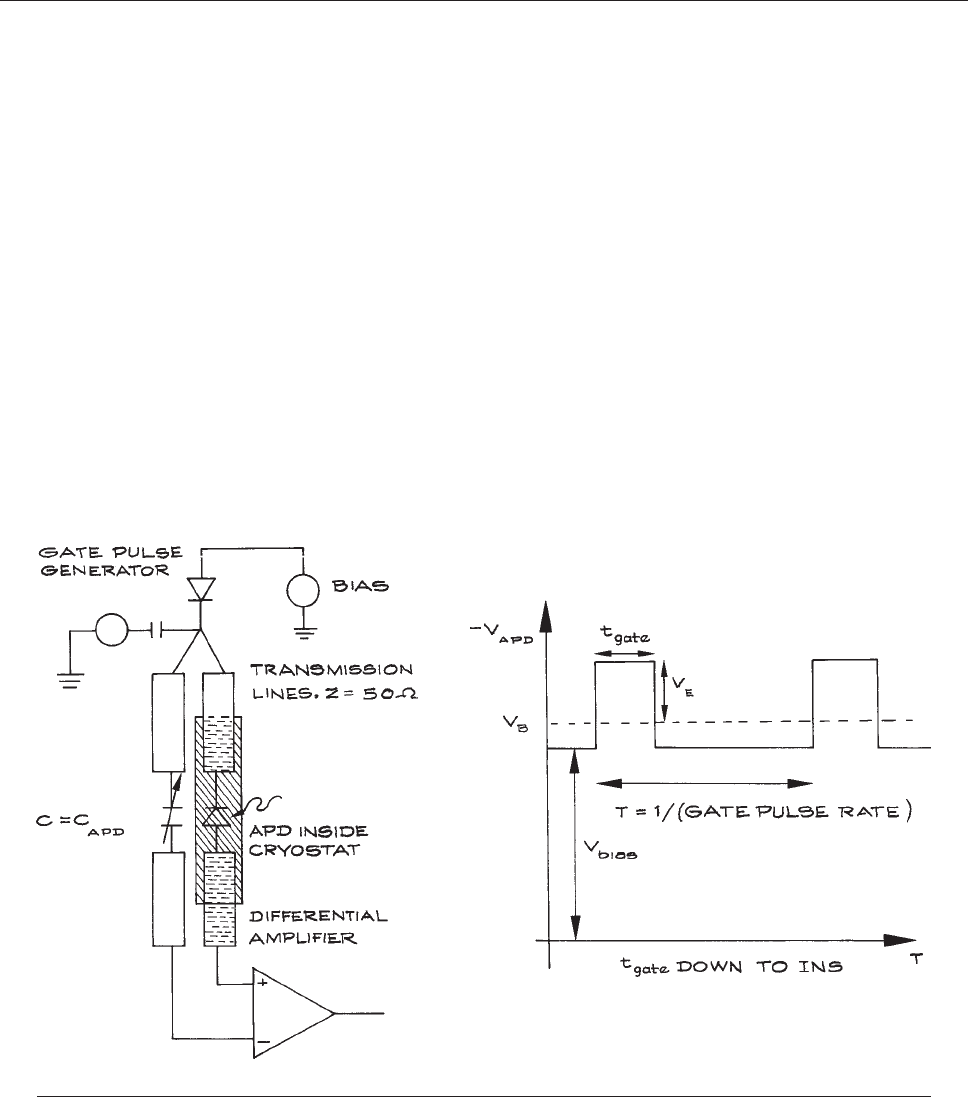
and operating characteristics of various photodiode
detectors has been given by Gowar.
34
Avalanche photo-
diodes are available from Advanced Photonix, L aser
Components DG, OSI Optoelectronics, Pacific Silic on
Sensor, Perkin–Elmer Optoelectronics, and Sensors
Unlimited.
7.6.2 Geiger Mode Avalanche
Photodetectors
If an APD with a very low dark current is operated in
the Geiger mod e,
35–38
where the reverse-bias voltage V
R
is set greater than the diode breakdown voltage V
BR
,
then a single photon can trigger a substantial circuit
pulse. In other words, the current or voltage pulse they
produce from t he detection of a single photon is above
their noise levels. The internal gain of the APD can
reach 10
5
–10
6
. To prevent the diode from permanent
damage it must be operated with a ‘‘que nching’’ current,
which reduces the bias voltage to stop the avalanche
process. Otherwise the diode will conduct a l arge current
when it is biased above the breakdown voltage. It is
desirable to reduce the dark current by cooling the
APD. APDs operated in this way are true ‘‘single
photon’’ detectors, and can replace PMTs in many pho-
ton-counting applications.
Photodiodes using silcon, InGaAs/InP, InGaAs/Si and
HgCdTe have all been successfuly used in Geiger mode.
Complete Geiger-mode APD modules are available from
Perkin–Elmer Optoelectronics. Dark counts below 1 count
per second (CPS) have been reported for Perkin–Elmer
SLiK silicon APDs cooled to 20 °C, and dark counts belo w
250 cps are typically achievable with a cooled PerkinElmer
0.5 mm C30902S APD.
Anexampleofanoperatingarrangementforan
InGaAs-cooled Geiger-mode APD is shown in Figure
7.2
9. For operation in Geiger mode, the r everse bias is
Figure 7.29 Arrangement for operating a Geiger-mode APD.
39
PHOTOVOLTAIC DETECTORS 577

held just below the breakdown voltage (20–40 V). The
bias voltage is briefly gated above th e breakdown value
synchronously with the excitation process that i s
expected to gene rat e sin gle photons. Avalanche d oes
not generally occur unless an actual photon is detected.
The avalanche pr oc ess gene rate s a significant cur rent
pulse with peak current 1 mA. When the gat ing voltage
app lied to the APD is removed, the avalanche is quenched
because the APD is now below b reakd own, an d the cur-
rent pulse terminates.
7.7 DETECTOR ARRAYS
Arrays of individual photodetector elements, based on
photodiode, photoconductive, pyroelectric, microbolome-
ters, CMOS, and CCD elements, are widely available for
use in both the visible and the infrared. Such arrays are
useful in a variety of applications, such as spectral analy-
sis, image analysis, and position sensing.
7.7.1 Reticons
Multiple element linear arrays, often called ‘‘reticons,’’
are widely used in spectrographs. Light from the diffrac-
tion grating in such a n instrument falls on such an
array instead of on an exit slit. Arrays based on sili-
con, InGaAs, HgCdTe, PbS, and PbSe are available from
various manufacturers, including Advanced Photonix (Si),
Cal-Sensors (PbS, PbSe), Fermionics (HgCdTe, InGaAs),
Hamamatsu (Si, InGaAs), Kodak (Si), Perkin–Elmer Opto-
electronics (Si), SensArray Infrared (PbS and PbSe), and
Sensors Unlimited (Goodrich)(InGaAs). Silicon-based reti-
cons are linear CCD (charge coupled device) arrays. The
number of pixels in a linear detector can be as large as
10, 200, although 1024 or 2048 element arrays are most
common. Linear arrays can also be used for position
sensing.
7.7.2 Quadrant Detectors
Quadrant detectors (quads) are particularly useful in
laser-beam tracking and similar operations. These detec-
tors have four contiguous active elements with very little
inactive area between them, as shown in Figure 7.30(a) .
If
a light beam is centered on the detector, all four ele-
ments provide the same signal. By the use of a circuit,
such as the one shown in Figure 7.30(b), simultaneous
dis
play of the X and Y displacements of the bea m
from the center of the array can be obta ined. If the
signals from the four quadrants are A, B, C, and D in
the circuit shown i n Figure 7.30(b), then the relative
position
of the center of a circular illumination spot
can be calculated as:
x ¼
ðB þ DÞðA þ CÞ
A þ B þ C þ D
ð7:18Þ
y ¼
ðA þ BÞðC þ DÞ
A þ B þ C þ D
ð7:19Þ
The displacements x and y are fractions, which would have
to be calibrated by moving the beam centroid by a known
distance in a particular application.
Silicon quadrant detectors are available from Advanced
Photonix, Electro-Optical Components, OSI Optoelectronics,
and Silicon Sensors. Ge and InAs quad detectors are available
from Judson. Infrared HgCdTe quad detectors are av ailable
from Judson and Raytheon Vision Systems (formerly Santa
Barbara Research Center). In some simple situations, small
one-dimensional deflections of a light spot can be measured
by focusing the light spot on the edge of a razor blade, and
measuring the amount of light reaching a photodetector
placed beyond the sharp edge, as shown in Figure 7.31.
7.7.3 Lateral Effect Photodetectors
Lateral effect photodetectors (LEP) also provide output
signals that allow determination of the position of the
centroid of an incident light spot on the surface of the
LEP. They are therefore useful in experiments in which a
laser beam is deflected, and the deflection needs to be
detected, or they can be used in general laser-beam track-
ing applications. The LEP, in its simplest form, consists of
a surface resistive layer on top of a p–n junction substrate,
and has two lateral electrodes. When a light ray is received,
the resulting photo-induced currents diffuse separately
along the junction faces and recombine at a distance from
their origin of separation. The analytical solution of the
diffusion equation, representing the potential on the sur-
face of the LEP on the two sides, varies approximately
578 DETECTORS
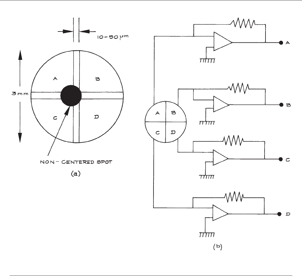
linearly with respect to the incident position of the light
and the received power. The dependence on the received
power can be eliminated by normalizing with respect to the
total received power.
Normally, the fabrication of a two-dimensional LEP can
be divided into: (1) Wallmark dual-axis, (2) duo-lateral, and
(3) tetra-lateral structures.
40
Most commercial LEPs use the
duo-lateral type, shown schematically in Figure 7.32, since it
p
rovides the best linearity. Most of f-the-shelf LEPs hav e a
0.1% linearity error near the center region and the error
increases to 1% when approaching the edges. These devices
can detect the movement of a small light spot with micro-
meter or smaller precision. Lateral ef fect photodetectors with
preamplifiers are available from Electro-Optical Systems
(EOS), On-Trak, and Pacific Sensor . LEP bundles, including
post-amplification circuits, are available from Hamamatsu,
Figure 7.30 (a) Schematic diagram showing the construction of a quadrant
detector; (b) a circuit suitable for providing X and Y beam-deflection readouts
in a beam-centering or beam-tracking application.
DETECTOR ARRAYS 579
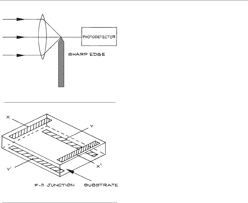
Newfocus, and Thorlabs. In contrast to quadrant detectors,
LEPs are superior for their large linear region and small
internal resistance. The latter results in a short response
time, but a larger noise equivalent power. This implies that
quadrant detectors are better in applications that involve
weak received power, such as feedback sensors in remote
sensing applications. LEPs, on the other hand, are advanta-
geous as local kinematic sensors.
7.7.4 Imaging Arrays
Two-dimensional arrays of photodetector generally show
up in imaging systems. Complementary Metal-Oxide-
Semiconductor (CMOS) or CCD arrays based on silicon
are common in visible and near-infrared digital camera
systems. These array detectors can be thought of as equiva-
lent to an array of ‘ ‘pho ton-buckets.’’ The number of photons
detected at each array element produces a corresponding
number of electron–hole pairs. The electrons at each pixel
are trapped in a potential well, equiv alent to a small capacitor ,
and then read out sequentially by moving these electrons from
well to well.
41
InGaAs arrays provide performance between
0.9 lmand2.2lm. Infrared cameras for operation beyond
10 lm use arrays of microbolometers (see later). A compre-
hensiv e list of suppliers of array detectors in dif ferent spectral
regionsisavailable.
25
In consumer digital cameras, CCD and CMOS arrays are
the standard image detectors. Such cameras generally con-
tain all the electronics to read out the signals from the array
elements and store them in digital format, including color
and grayscale. The most common image format from such
cameras is .jpeg. The number of available pixels in such
cameras continues to increase, and formats with more than
16 million pixels are already available. Typical formats are:
1216 3 912 (1 megapixel), 1600 3 1200 (2 megapixel),
2240 3 1680 (4 megapixel), and 4064 3 2704 (11.1 mega-
pixel). The actual number of pixels in these arrays is larger
than the number specified by the resolution, because some
dark array elements are used for reading out the image. It is
worth noting that the effective resolution of a good-quality
film camera is at least 20 million pixels, detemined by the
‘‘grain’’ size in the film. The image stored by such cameras
is a single ‘‘frame,’’ captured as the average illumination of
each pixel over the exposure time chosen. Color is gener-
ally captured by having a filter array placed in front of the
pixels. The filter array usually has alternating rows of red/
green and blue/green filters, a so-called ‘‘Bayer pattern.’’
The image is processed using the signals from adjacent
pixels to provide a best estimate of the color at each pixel,
a process called demosaicing.
42
Advanced digital cameras
use Foveon X3 technology (Foveon, Inc., 2820 San Tomas
Expressway, Santa Clara, CA 95051), in which the active
pixel elements are embedded in a silicon matrix at different
depths. Because blue, green, and red light penetrates differ-
ent distances into silicon, the camera acts as though it has
three sequential blue, green, and red imaging arrays. The
quantum efficiency, sensitivity, maximum frame rate, satu-
ration light level, and dynamic range of CCD and CMOS
Figure 7.31 Schematic arrangement for measuring the
deflection of a focused light beam by using a knife edge.
Figure 7.32 Schematic construction of duo-lateral lateral
effect photodetector (LEP).
580 DETECTORS
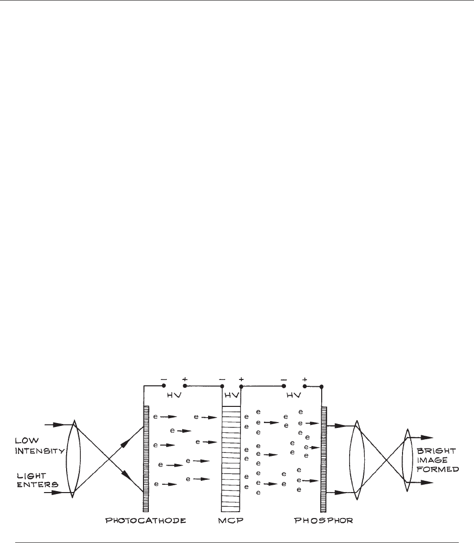
imagers vary and manufacturers’ data sheets should be con-
sulted. Of the two, CCD imagers are generally more sensi-
tive, and have lower noise than CMOS imagers; CMOS
imagers on the other hand use less power and are less
expensive. As CCD imagers cannot be gated electronically,
if short exposures are required, then a mechanical shutter is
needed. Infrared imaging arrays with response from 0.5–14
lm, based on InSb and HgCdTe, are available from Ray-
theon Vision Systems; HgCdTe imaging arrays are avail-
able from Sofradir.
The experimentalist who wishes to work with CCD or
CMOS imaging arrays that are not already integrated into a
complete camera system should consult the suppliers of such
devices, such as K odak or Sony. This is a specialized endeavor.
If it is desired to have complete control of image capture as a
digital file directly into a computer , then a digital camera with
compatibility with a framegrabber card is needed. Framegrab-
ber cards usually utilize a special interface standard called
Cameralink, which is used by all major scientific camera man-
ufacturers. It allows for data rates in excess of 2 Gb/s. Scien-
tific cameras differ from consumer ones in that they provide
uncompressed frames at high frame rates, such as 210 fps in
the case of the Imperx IPX-210. These uncompressed frames
allow for adva nced image analysis in Labvie w, Matlab, and
other image-processing applications.
43
The primary manufac-
turers of framegrabbers are Imperx and National Instruments,
while cameras can be acquired from Imperx, Dalsa, Pulnix,
and Flir. It is worth noting that some cameras have now
come on the market that use a gigabit Ethernet standard
to transmit frames, the Imperx IPX-2M30H-GC
(1920 3 1080 30 fps color) being one example.
7.7.5 Image Intensifiers
In some applications, for example in astronomy or
night vision, it is desirable to obtain an image that can
be viewed by the human eye, or with a digital camera,
when the light levels available are extremely low. Low-
light-level imaging can be carried out with an image inten-
sifier. Image intensifiers work by using weak visible or
near infrared light to liberate photoelectrons from a GaAs
photocathode, which has a high quantum efficiency to
about 920 nm. The photoelectrons are accelerated onto a
microchannel plate, where secondary electron ampli-
fication increases their number. The amplified electron
stream then falls onto a phosphor screen where the image
is rendered visible. Figure 7.33 shows the principle of oper-
atio
n. As image intensifiers have evolved, photocathode
materials and the electron multiplication stages have
improved. The earliest image intensifiers were called gen-
eration 0, G0, which used S1 photocathodes, G1 tubes used
an improved S-20 photocathode. G2 and G3 tubes used a
MCP for electron multiplication, typical amplification
gains can be as high as 10
7
. G2 tubes use an S-25 photo-
cathode with typical peak sensitivity of 50 lA/W. G3 tubes
use GaAs or GaAsP photocathodes with typical sensitivity
of 200 lA/W. Nowadays only G2 and G3 tubes should be
considered for use. Manufacturers of image-intensifier
Figure 7.33 Operating arrangement of a microchannel plate image intensifier.
DETECTOR ARRAYS 581

tubes include Electrophysics Corporation, Hamamatsu,
ITT Night Vision, Photek, Photonis, and Thales.
7.8 SIGNAL-TO-NOISE RATIO
CALCULATIONS
7.8.1 Photomultipliers
In many applications using photomultiplier tubes, the
anode pulses are integrated to give a fluctuating analog
current. The shot noise originating at the photocathode
is, from Equation (7.1):
<i
2
N
>
c
¼ 2eð<i
c
> þ <i
d
>ÞDf ð7:20Þ
where <i
c
> is the average photocathode current produced
by a light source and <i
d
> is the average photocathode
dark current. This noise is multiplied by the amplification of
the electron number by interaction with the N dynodes of
the tube. If each dynode has a secondary emission mul-
tiplication efficiency d the overall gain of the tube is G:
G ¼ d
N
ð7:21Þ
Because of statistical fluctuations in the secondary
emission process and, in addition, because electrons can
originate thermionically from the dynodes, the noise at the
anode is further increased by a noise factor F. The overall
noise appearing at the anode is:
<i
2
N
>
A
¼ 2eG
2
F <i
c
> þ <i
d
>ðÞDf ð7:22Þ
For d ¼ 4, and a 14 stage tube, G ¼ 2.6 3 10
8
, and
typically F ’ dðd 1Þ¼1:08.
A photomultiplier is a current source: to convert this
current to a detected voltage the amplified photoelectron
current passes through an anode resistor of value R. This
anode resistor may be part of the photomultiplier circuit, or
may be provided in whole or in part by the input impe-
dance of a following amplifier stage. The Johnson noise
from the resistor is:
<i
2
N
>
R
¼
4kTDf
R
ð7:23Þ
To optimize detection of a signal, it is common practice
to amplitude modulate the signal at some angular fre-
quency x
m
so as to permit synchronous detection at this
frequency (see Section 6.8). The optical power reaching
the photocathode can be represented in this case as:
P ¼ P
0
1 þ m sin x
m
tðÞð7:24Þ
where m is a modulation parameter.
The average photocathode current is:
<i
c
> ¼
egP
0
hm
ð7:25Þ
and:
i
c
ðtÞ¼<i
c
>1þ m sin x
m
tðÞð7:26Þ
At the anode, the time-varying part of this current is:
i
s
tðÞ¼<i
c
>Gm sin x
m
t: ð7:27Þ
The signal-to-noise ratio (S/N) at the input to the following
electronics is therefore:
<i
2
s
>
<i
2
N
>
A
þ <i
2
N
>
R
¼
<i
2
c
>G
2
m
2
=2
2eG
2
Fð<i
c
> þ <i
d
>ÞDf þ 4kTD f =R
ð7:28Þ
The noise from the photomultipler tube is usually suffi-
ciently large that the Johnson noise can be neglected. If
it is assumed that <i
d
> <i
c
>, then for m ¼ 1 and S/N ¼ 1
we have, from Equations (7.25) and (7.28):
ðP
0
Þ
min
¼
2hm
g
ffiffiffiffiffiffiffiffiffiffiffiffiffiffiffiffiffiffi
F<i
d
>Df
e
r
ð7:29Þ
Example: Typical values for a good photomultiplier will
be g ¼ 0:2, F ’ 1, <i
d
> ’ 10
15
A. For a 530 nm source,
Equation (7.29) gives (P
0
)
min
¼ 3 3 10
–16
W.
7.8.2 Direct Detection with p–i–n
Photodiodes
The shot noise from a p–i–n photodiode is:
<i
2
N
>
SN
¼ 2e <i
s
> þ i
d
ðÞDf ð7:30Þ
582 DETECTORS

where <i
s
> is the average signal current, and i
d
is the dark
current (usually specified, for a low-noise photodiode, in
units of nA or pA).
The average signal current is, in a similar way to Equa-
tion (7.25),
<i
s
> ¼
egP
0
hm
ð7:31Þ
where g is the quantum efficiency, which is much larger
than for a photomultiplier: values of 0.7–0.8 are common.
For the simple equivalent current of the detector shown in
Figure 7.34, there is an additional Johnson noise contribu-
tion of magnitude:
<i
2
N
>
JN
¼
4kTDf
R
ð7:32Þ
The overall S/N ratio for direct detection of an unmodu-
lated signal is:
<i
2
s
>
<i
2
N
>
SN
þ <i
2
N
>
JN
¼
ðegP
0
=hmÞ
2
R
2eRðegP
0
=hm þ i
d
ÞDf þ 4kTDf
ð7:33Þ
This S/N ratio would be reduced by a factor m
2
/2 for a
modulated signal (cf. Equation 7.28). If shot noise domi-
nates over dark current and Johnson noise, then the shot-
noise-limited S/N ratio is:
S
N
¼
gP
0
2hmDf
ð7:34Þ
In a practical application using a photodiode there will
be additional stages of electronic amplification that add
noise. It is common to characterize the effect of an elec-
tronic circuit on the noise by its noise figure, F
N
.
The noise figure can be defined conveniently as:
F
N
¼
noise power at output of circuit
noise power at the input 3 amplifier power gain
ð7:35Þ
For input Johnson noise the mean-square, amplified, out-
put noise current is:
<i
2
N
>
AJN
¼
4kTGDf
R
ð7:36Þ
where G is the power gain of the amplifier within the
frequency band being considered. The actual output
mean-square noise current is:
<i
2
N
>
actual
¼
4kTGF
N
Df
R
ð7:37Þ
It is as if the amplifier were noiseless with the input John-
son noise increased by the noise figure.
The noise figure is frequently quoted in dB, a noise
figure of 3dB would represent a doubling of the out-
put noise over the value expected from a noiseless
amplifier. The term noise temperature T
i
is also used,
defined by:
F
N
¼ 1 þ
T
i
T
ambient
ð7:38Þ
Figure 7.34 Equivalent circuit of a p–i–n photodetector.
S/N RATIO CALCULATIONS 583

Example: We illuminate an InGaAs photodiode with a
responsivity of 0.8 A/W at 1.3 lm with a power of 10 lW.
The system bandwidth is 100 MHz, the dark current is
5 nA (equivalent to 0.5 pA Hz
–1/2
). We assume that the
amplification electronics has a noise figure of 6 dB (rel-
ative to a 50 ohm input). We note the following:
Received power P
0
¼ 10
–3
3 10 mW ¼ 10 lW
Signal current <i
s
> ¼ 8 lA
Dark current <i
d
> ¼ 5 nA (in this case dominated by <i
s
>)
Signal power ¼ (<i
s
>)
2
R ¼ 3.2 nW
Shot noise power ¼ 2e(<i
s
>+<i
d
>) dfR ¼ 1.28 3
10
–14
W
Johnson noise power ¼ 4kTdf ¼ 4(1.38 3 10
–22
)
(300)(10
8
) ¼ 1.66 pW
Effective Johnson noise power including noise Figure ¼
10
0.6
3 1.66 pW ¼ 6.6 pW.
In this case the Johnson noise is dominant, the effective
S/N ratio is:
S
N
¼
3:2 3 10
9
6:6 3 10
12
¼ 485
7.8.3 Direct Detection with APDs
In an APD there is a multiplication of the number
of charge carriers by a factor M. This m ultiplication
can result from secondary ionizations produced by
both electron s an d holes. It is desirable that one or other
of these charge carrier s s hould have a significantly
greater secondary ionization coefficient
b
than the
other.
44
The current in an APD incre ases by the factor
M, but the associated shot noise increases further,
because i n a given avalanche process M will fluctuate,
taking values M, M 6 1, M 6 2, etc. The mean-square
noise current thereby increases, not by a f actor M
2
,but
by a fa ctor FM
2
,whereF is called the noise factor.In
silicon APDs, F typically lies in the range 2–20. There-
fore, the shot noise becomes:
<i
2
N
>
1
¼ 2eFM
2
<i
s
> þ i
d
ðÞDf ð7:39Þ
Both photo- and dark-generated carriers contribute to
the shot noise. The overall S/N ratio is modified from
Equation (7.33) and becomes:
<i
2
s
>
<i
2
N
>
SN
þ <i
2
N
>
JN
¼
M
2
ðegP
0
=hmÞ
2
R
2eRFM
2
ðegP
0
=hm þ i
d
ÞDf þ 4kTDf
ð7:40Þ
Equation 7.40 shows that the S/N ratio improves with
increasing multiplication as the Johnson noise contribution
becomes less important until the avalanche shot noise
becomes dominant. The avalanche-limited S/N ratio is:
S
N
¼
gP
0
2FhmDf
ð7:41Þ
a reduction of the signal-to-noise ratio from the quantum-
limited value by the noise factor.
The NEP can be computed for both p–i–n photodiodes
and APDs by setting S/N ¼ 1 in equations like (7.33) and
(7.40) and thereby the minimum input power for S/N ¼ 1
is determined. For P
0
¼ P
min
, we expect the dark current to
be larger than the signal current, so Equation 7.40 becomes:
S
N
¼
ðMegP
0
=hmÞ
2
ð2eFM
2
i
d
þ 4kT=RÞDf
ð7:42Þ
For S/N ¼ 1 and a 1 Hz bandwidth, P
0
¼ P
min
¼ NEP,
which gives, for an APD:
NEPðWHz
1=2
Þ¼
hm
Meg
ffiffiffiffiffiffiffiffiffiffiffiffiffiffiffiffiffiffiffiffiffiffiffiffiffiffiffiffiffiffiffiffiffiffiffiffi
2eFM
2
i
d
þ 4kT=R
q
ð7:43Þ
The equivalent result for a p–i–n diode can be obtained by
setting M ¼ F ¼ 1.
Example. For an InGaAs APD with F ¼ 10, M ¼ 100,
R ¼ 50 X, i
d
¼ 2 nA, and responsivity 0.8 A/W, the
quantum efficiency is:
g ¼
0:8ð6:626 3 10
34
Þð3 3 10
8
Þ
ð1:6 3 10
19
Þð1:55 3 10
6
Þ
¼ 0:64
From Equation 7.43 the NEP is:
NEP WHz
1=2
ð2 3 1:6 3 10
19
3 10
5
3 2 3 10
9
þ 4 3 1:38 3 10
22
3 300=50Þ
1=2
0:8 3 100
¼ 4:7 3 10
13
WHz
1=2
Note that in this case the thermal noise is dominant.
584 DETECTORS

7.8.4 Photon Counting
For the detection of very low light levels where photomul-
tipliers or Geiger-mode APDs can be used, the technique
of photon counting is the most sensitive technique. Sup-
pose that the signal to be detected corresponds to a photon
flux at the detector of N
p
per second. This corresponds to a
detected count rate of N
s
¼ gN
p
per second. Along with
this goes a dark count rate of N
d
per second. If the detected
counts are integrated for T seconds the total number of
counts is:
N
T
¼ðN
s
þ N
d
ÞT ð7:44Þ
Since the number of counts observed in a given integra-
tion interval fluctuates statistically, then, for a Poissonian
distribution, the standard deviation of the number of counts
observed is N
SD
¼
ffiffiffiffiffiffi
N
T
p
. Thus the counts recorded during
‘‘signal’’ intervals can be written as:
N
T
¼ðN
s
þ N
d
ÞT 6
ffiffiffiffiffiffiffiffiffiffiffiffiffiffiffiffiffiffiffiffiffiffiffiffi
ðN
s
þ N
d
ÞT
p
ð7:45Þ
If the dark counts alone are integrated over the same time
interval T the total number of counts can be written as:
N
D
¼ N
d
T 6
ffiffiffiffiffiffiffiffiffi
N
d
T
p
ð7:46Þ
The signal-to-noise ratio of the photon-counting process
is determined by the difference between N
T
and N
D
, taking
into account their respective standard deviations. It can be
characterized as:
S
N
¼
N
s
T
ffiffiffiffiffiffiffiffiffiffiffiffiffiffiffiffiffiffiffiffiffiffiffiffiffiffi
ðN
s
þ 2N
d
ÞT
p
ð7:47Þ
This signal-to-noise ratio can be continuously improved
by extending the integration time. The ‘‘signal’’ and
‘‘dark’’ counting intervals can be alternated by chopping
or ‘‘gating.’’
45
Example. Consider a dark count rate of 100 /s and a
signal count rate of 1 /s. A signal-to-noise ratio of 10 will
be achieved when T=
ffiffiffiffiffiffiffiffiffiffiffi
201T
p
¼ 10, i.e. after an integration
period of about 6 hours. It should be noted that if the count
rates are too high, so that some counts are missed – so
called ‘‘pile-up’’ effects,
46
then these calculations are
slightly modified.
7.9 PARTICLE AND IONIZING
RADIATION DETECTORS
For charged-particle energies up to a few tens of keV there
are two detection schemes in wide use. The particles can
be collected at a metal surface and the resultant electrical
current measured directly, or they can be detected by col-
lecting the slower secondary electrons that are ejected
from a metal surface by impact of the primary particle.
Charged particles can also be detected with photographic
emulsions, scintillators, and various solid-state devices.
Emulsions have largely been supplanted by the methods
mentioned above, and solid-state devices are only suitable
for the detection of high-energy particles (above 30 keV).
Table 7.5 lists the properties of common particle detectors.
Th
e collector for the direct detection of a current of
charged particles is called a Faraday cup. Typical designs
are illustrated in Figure 7.35. These simple collectors are
co
nnected directly to a current-measuring device and are
useful at currents down to the detection limits of modern
electrometers – about 10
–14
A. A properly-designed Faraday
cup does not permit secondary electrons to escape. For a
positiv e-ion collector, the loss of a secondary electron
appears to the current-measuring instrument as an additional
ion, while for an electron collector the loss of each secondary
cancels the effect of an incident primary electron. To prevent
the escape of secondary electrons, the depth of a Faraday cup
should be at least fiv e times its diameter. A suppressor
Table 7.5 Particle detectors
Particle
Detector
Output Signal
Level
Charge-Collection
Time
Ge 2.8 eV/electron–hole pair 0.1–10 ns
a
Si 3.5 eV/electron–hole pair 0.1–10 ns
a
Electron
multiplier
10
6
–10
8
electrons/
incident electron
0.5–1 ns
Microchannel
plate
10
3
–10
4
electroncs/
incident photon
0.1 ns
Scintillator:
Plastic ~1 photon/3keV 0.1–10 ns
Alkali halide ~1 photon/3keV 1 ls
Gas-filled tube 25–35 eV/ion pair 0.01–5 ls
a
For narrow depletion depth.
PARTICLE AND IONIZING RADIATION DETECTORS 585
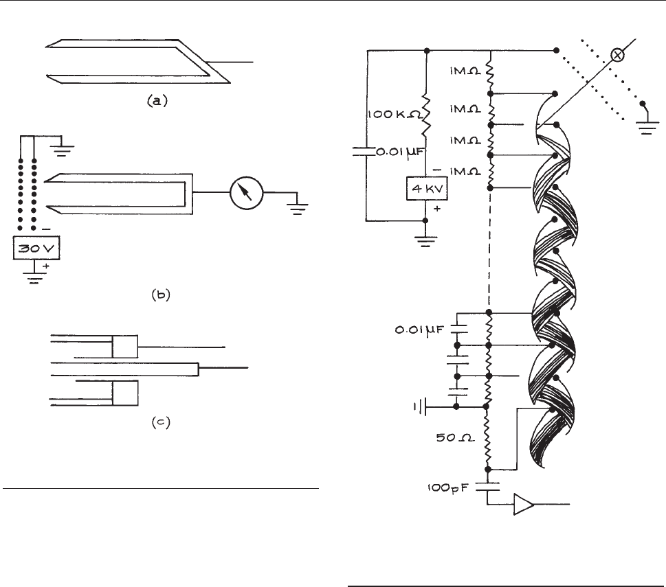
aperture or grid biased to about 30 V in front of a Faraday
cup effecti v ely pre v ents the escape of most secondaries.
A grounded grid in front of the suppressor as illustrated
in Figure 7.35(b) prevents field penetration from the sup-
pressor
in the direction of the incident current source.
When a particle beam must be aligned and sharply
focused, a concentric pair of collectors [Figure 7.35(c)]
is useful. With this arrangement the beam-focusing ele-
ments
are adjusted to maximize the ratio of current to
the inner cup in relation to the current to the outer cup.
Charged-particle currents of less than 10
–14
A can be
detected with an electron multiplier, which is like a photo-
multiplier without the photocathode. As illustrated in
Figure 7.36 , these devices have an internal dynode struc-
ture.
Secondary electrons produced by impact of a particle
on the first dynode are accelerated towards the second
dynode through a potential drop of 100–300 V. The impact
of these electrons results in a number of secondaries that
are in turn accelerated into the third dynode, and so on. The
secondary emission coefficient of the dynodes is typically
about three electrons per incident particle; the impact of a
single particle on a multiplier with n electrodes results in a
pulse of about 3
n
electrons.
Electron multipliers are available with 10 to 20 dynodes
to provide gains of 10
6
to 10
9
. The dispersion in time of the
shower of electrons from the last dynode is on the order of
Figure 7.36 An electron multiplier. Electrical connections
shown are appropriate for detecting positive ions. Grids at
the entrance of the multiplier prevent the escape of
secondary electrons.
Figure 7.35 Faraday cup designs. Design (b) has a grid
biased to suppress secondary electron emission. Design (c)
has a double cup for aligning and focusing a beam.
586 DETECTORS

10 ns. The corresponding current through a 50 ohm meas-
uring resistor ranges from 800 lV to 800 mV, which is
easily detected with modern pulse-counting electronics.
Furthermore, if time resolution is not required, the output
current from an electron multiplier can be measured
directly with an electrometer.
The electrodes of an electron multiplier are fabricated
of a material that has a high work function – typically a
Be–Cu alloy that has been ‘‘activated’’ by some proprietary
process. The high work function is desirable because it
inhibits thermionic emission that would result in noise
pulses at the multiplier output. On the other hand, incident
particles must have energies in excess of a few hundred eV
to assure efficient secondary emission. When working with
lower-energy particles, it is necessary to provide an accel-
eration stage at the multiplier input. For incident particles
with energies greater than 300 eV, the detection efficiency of
an electron multiplier can exceed 90%.
For the detection of positive ions, an electron multiplier is
usually operated with the first dynode at a high negative
potential and the last dynode near ground potential, as in
Figure 7.36. This arrangement provides acceleration of inci-
de
nt ions. For electrons or negative ions, the cathode is
usually biased positive by a few hundred volts and the last
dynode is at a high positive potential relative to ground, as in
Figure 7.37. In this latter configuration, it is only convenient
to
operate in a pulse-counting mode, since the detection
electronics must be electrically insulated from the measur-
ing resistor. Ordinarily, the multiplier output is coupled to
the pulse-counting electronics via a high-voltage disk
ceramic capacitor of about 100 pF. A problem sometimes
encountered with this arrangement is that sparking between
dynodes or across dynode resistors gives rise to large high-
frequency transients that are transmitted through the cou-
pling capacitor and damage the electronics. This problem
can be cured by coupling the output of the multiplier to the
electronics through a transformer that will attenuate large
pulses because of saturation of the ferrite core material. A
suitable transformer can be produced by making a 10-turn
bifilar winding of well-insulated wire on a ferrite core (e.g.
Ferroxcube), as illustrated in Figure 7.38.
47
The number of
turns and their position must be carefully adjusted to assure
a proper impedance match between the multiplier and the
electronics.
The output current from an electron multiplier is limited
by the current available from the resistive voltage divider
Figure 7.37 A channel electron multiplier. Electrical connections shown are for the
detection of electrons.
PARTICLE AND IONIZING RADIATION DETECTORS 587
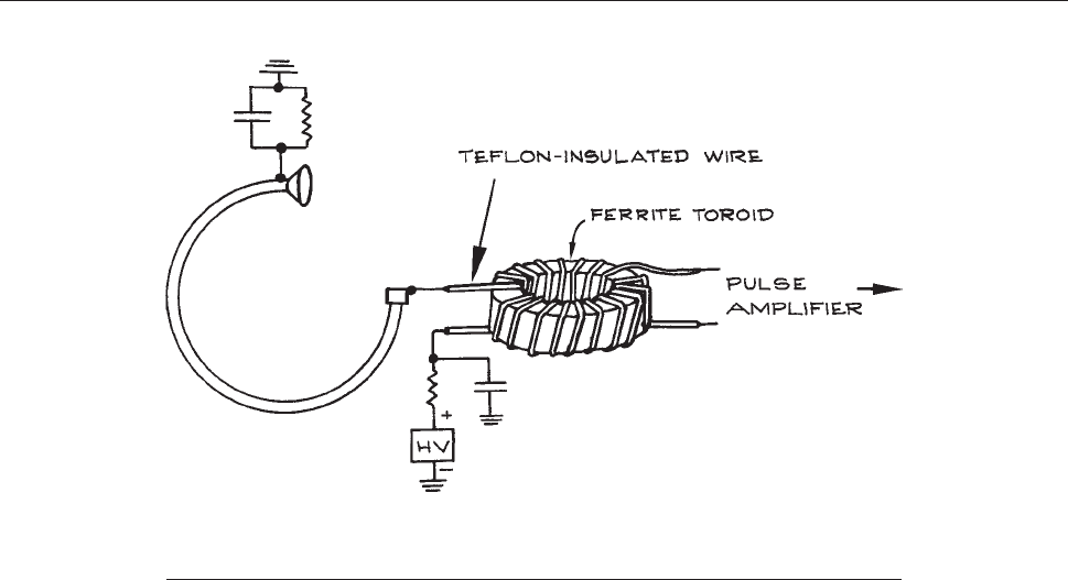
that establishes the potential of the dynodes. To ensure that
the gain of a multiplier is not reduced because of depletion
of the dynode charge, the maximum output current should
be at least an order of magnitude less than the current
drawn by the dynode resistor chain. For CEMs, the output
current should be an order of magnitude less than the cur-
rent from the high-voltage supply through the (typically
10
9
ohm) resistance of the channel.
An important variant of the electron multiplier uses a
continuous dynode as illustrated in Figure 7.3 7.Theseare
channe
l electron multipliers (CEM) or channeltrons.
They are glass tubes with semiconducting i nner surf aces.
The end-to-end resistance is about 10
9
ohm. In operation,
a potential of about 3 kV across the CEM yields a gain of
about 10
8
. Channel electron multipliers have the advant-
age of small size (about 50 mm long), low cost, and
ruggedness. Recently, monolithic ceramic CEMs have
become available from OptoTechn ik. These consist of a
ceramic block with an interior serpentine channel. Many
con figurations a re avai labl e, w ith entrance apertures as
small as a few mm
2
to more than 1 cm
2
. The overall
volume ranges from 1 to 5 cm
3
. The monolithic ceramic
CEMs are very robust. They have found wide use in
rocket-borne instruments, where force s at l aunch can
exceed 30 G.
The gain of a CEM is determined, n ot by the absolute
size, but rather by the ratio of the length of the channel to
the diameter. This ratio is about 50 for a conventional
CEM. Very small CEMs are available in close-packed
arrays. Each channel is a few micrometers in diameter
and a few mm long. The arrays, known as microchannel
plates or MCPs, are available i n sizes up to 10 cm on a
side. Bec ause the length-to-diameter ratio is only about
20, microchannel plates are usually stacked in pairs to
provide easily detected charge pulses. Owing to the small
size of the channel, the c harge cloud through a chann el is
temporally much more compact than in a full-size CEM.
The charge cloud is delivered in about 1 ns. With lead-
ing-edge discrimination it has been possible to time the
arrival of a charged particle at the detector with a reso-
lution of a few hundred p icoseconds.
Microchannel plates are used as position-sensitive
detectors of electrons and ions at energies up to at least
10 keV. A particle striking the front of the plate triggers
an electro n avalanc he in only one channel. The position
of the charge cloud emitted at the output of a channel can
Figure 7.38 A coupling transformer between an electron multiplier and a sensitive pulse
amplifier. Properly constructed, a transformer will faithfully transmit signal pulses while
attenuating large noise pulses.
588 DETECTORS
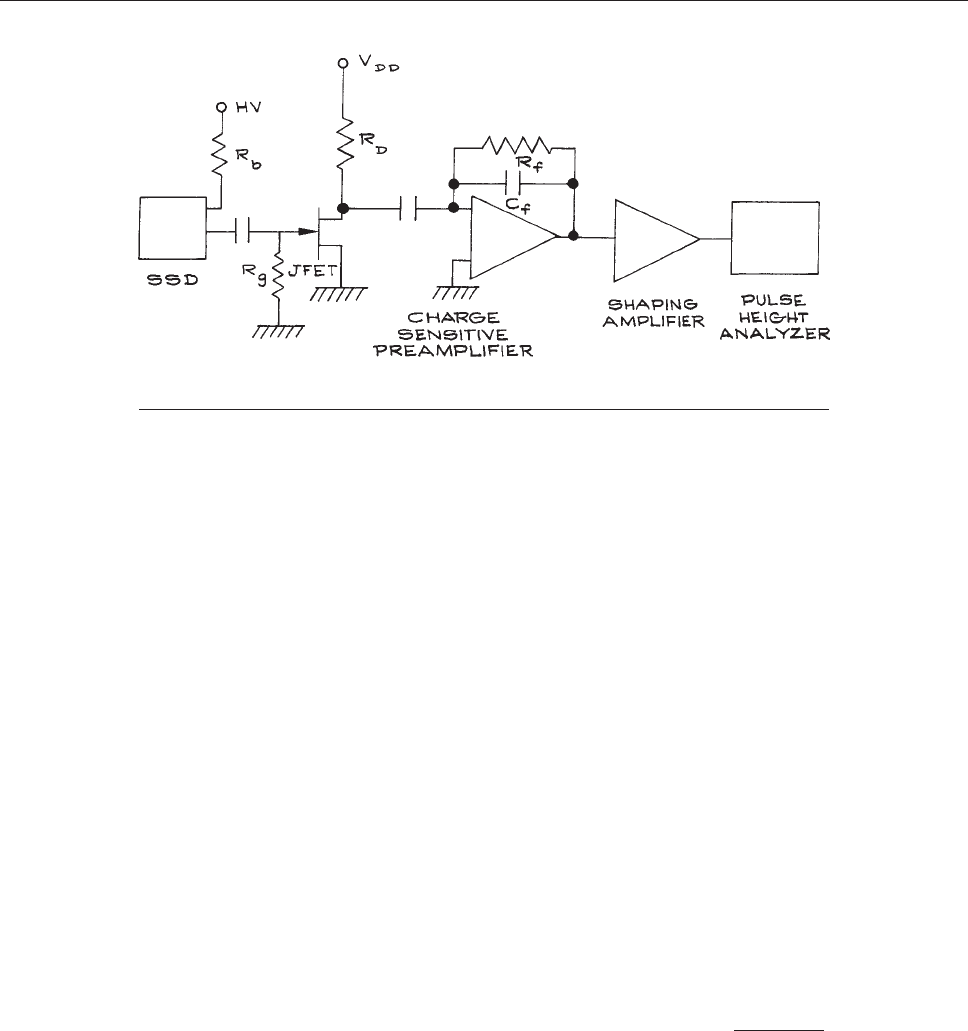
be loc ated with an accuracy approaching the diamet er of
the channel . Bo th one -dime nsion al and two-dimensional
position information can be extracted. A number of meth-
ods have been developed to obtain position information.
48
The most straightforward scheme is to provide an array of
collectors each with its own pulse amplifier and counter.
This is the most robust method, but expensive and
impractical if the full resolution of the microchannel plate
is to be realized – a standard 2.5 cm round MCP can
potentially provide more than 10
4
pixels. Many posi-
tion-sensitive detectors employ a resistive strip anode
across the ba ck o f a stacked pair of MCPs. The arrival
of a charge pulse at a point on the anode is detected
simultaneously as a pulse at each end or eac h c orne r of
the anode, a nd the position is determined from the ratio of
the pulse heights.
7.9.1 Solid-State Detectors
A solid-state detector (SSD) converts particle energy to
charge that is then collected and amplified. Silicon detec-
tors convert every 3.6 eV of particle kinetic energy to a
single electron–hol e pair. The energy resolution of a SSD
depends on the charge generated by the incident particle,
the noise generated by the d et ector, an d the electronic
circuits to which the output of the detector is connected.
Resolution is also affected by the charge generat ion
mechanism within the detector. Charge generation falls
within a purely statistical process and one determine d b y
a constant energy loss per electron–hole pair creation.
There is also the variable energy loss in the thin window
of the detecto r and the efficiency of charge collection as a
function of the geometry of the e le ctron –ho le p air pro-
duction. The arrangement of an SSD with FET amplifier
followedbyashapingamplifierandpulse-heightana-
lyzer is shown in Figure 7.39.
The SSD is essen tia lly a reverse-biased diode wit h the
bias
voltage applied through a high resistance R
b
in series
with the voltage supply. The FET is used in the common
source (CS) configuration as a transconductance ampli-
fier (see also Chapter 6). There is a large gate bias resistor
R
g
from the gate to ground. The shaping amplifier
increases the amplitude of the signal from the FET output
and also transforms the output pulse into one with an
approximate Gaussian shape with rise-time s
r
and f all -
time s
f
.Normallys
r
and s
f
are set equal to a single time s.
The response of the shaping amplifier as a function of
frequenc y x is given by:
AðxÞ¼A
0
ðx=sÞ
1 þðx=sÞ
2
ð7:48Þ
where A
0
is the mid-band gain of the amplifier.
Figure 7.39 A solid-state detector with an FET amplifier followed by a pulse-shaping
amplifier and a pulse-height analyzer.
PARTICLE AND IONIZING RADIATION DETECTORS 589
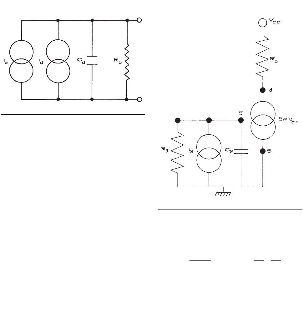
The SSD can be modeled as a current source i
s
in
parallel with a c apacitance C
d
that represents the effec-
tive capacitance of the SSD and the h igh voltage bias
resistor R
b
,asshowninFigure 7.40.Thecurrentsource
i
d
represents the leakage c urrent of the detector. The
small-signal model for the FET, shown in Figure 7.41,
includes the capacitance of the
gate-channel junction C
g
and the voltage-controlled c urrent source, g
m
v
gs
,where
g
m
is the transconductance of the JFET and v
gs
is the
gate-source signal voltage. Current flowing in the
reverse-biased gate-channel junction is represented by
the current source i
g
. There are various contributions to
both shot and Johnson noise in the arrangement shown in
Figure 7.41.Theseare:
(1)
Shot noise from the reverse-bias leakage current of the
SSD <i
2
N
>
SN1
¼ 2ei
d
Df
(2) Johnson noise from the series bias resistor <i
2
N
>
JN1
¼
4kTDf =R
b
(3) Shot noise from the JFET gate current <i
2
N
>
SN2
¼
2ei
s
Df
(4) Johnson noise from the gate bias resistor <i
2
N
>
JN2
¼
4kTDf =R
g
(5) Johnson noise from the channel resistance < i
N
2
>
JN3
¼
(4kTdfcg
m
), where for a long channel device c ¼ 2/3.
49
The current noise can be converted to voltage noise at the
gate of the FET by multiplying by the input impedance
of the FET. This impedance is dominated by C
d
and C
g
.
Because the noise sources are incoherent they are added in
quadrature. The total noise voltage is then:
<i
2
N
> ¼
1
4p
2
f
2
C
2
T
2ei
d
þ 2ei
s
þ
4kT
R
b
þ
4kT
R
g
þ 4kTcg
m
Df ð7:49Þ
where C
T
¼ C
d
+ C
g
. When this expression is integrated
over the response function of the shaping amplifier, the
noise voltage referred to the input of the FET is:
<V
2
N
> ¼
es
4C
2
T
ði
d
þ i
s
Þþ
kTs
2C
2
T
1
R
b
þ
1
R
g
þ
kT
2cg
m
s
ð7:50Þ
Figure 7.41 Small-signal equivalent circuit of an FET.
Figure 7.40 Equivalent circuit of a solid-state detector.
590 DETECTORS

The equivalent noise charge (ENC)
50
is obtained by multi-
plying this expression by C
T
, with the result:
ENC ¼
es
4
ði
d
þ i
s
Þþ
kTs
2
1
R
b
þ
1
R
g
þ
kTC
2
T
2cg
m
s
ð7:51Þ
As an example, let us evaluate this expression using the
experimental parameters of the Canberra fully depleted
passivated implanted planar silicon (PIPS) solid-state
detector, model FD 150-16-500 RM. The parameters of
the 2SK152 low-noise n-channel JFET are used to evaluate
the noise contribution from the JFET. A time constant of
10
–6
s was used for the shaping parameter. Below is a list
of the magnitudes of the parameters:
s ¼ 10
–6
s
i
d
¼ 166 nA
i
s
¼ 5nA
T ¼ 300 K
C
d
¼ 50 pF, C
g
¼ 15 pF, C
T
¼ 65 pF
R
b
¼ 108 ohm
R
g
¼ 108 ohm
g
m
¼ 30 mA/V
Additional Considerations. In order to transfer the
maximum energy from the detector to the JFET, the input
impedance of the JFET should be matched to the output
impedance of the SSD. This means that a transistor with
C
g
¼ C
d
should be chosen and stray capacitance
eliminated. The ratio of energy transferred to theoretical
maximum energy transfer is given by 4 x/(1 + x)
2
, where x
is the ratio of detector to gate capacitance, C
d
/C
g
. The
choice of the shaping constant s is an important factor in
the ENC, but it is also important to recognize that s fixes
the maximum count rate. For s ¼ 10
–6
s, the maximum
asynchronous count rate that can be accommodated with
90% efficiency is 100 kHz. The temperatures of the
SSD and JFET can be controlled. In this analysis the
temperature of the SSD and JFET are assumed equal,
however it is possible to independently cool one or the
other. The leakage current of the Canberra PIPS detector
is a strong function of temperature and is given by
i
d
¼ 63 10
9
2
T92ðÞ=5
ð7:52Þ
7.9.2 Scintillation Counters
Scintillation counters allow the detecti on of ionizing radi-
ation (X-rays, c-rays), and energetic particles (protons,
neutrons, muons, pions, etc.) by conversion of their
energy into visible light. A typical s cintillation counter
uses a fluorescent solid or liquid that converts a nonioniz-
ing photon or energetic particle into a flash of visible
light. The visible light is generally detected with a photo-
multiplier with a large-area photocathode placed in close
proximity to the scintillation m aterial. Scintill ators are
often made of plastics impregnated with a fluorescent
dye. The intensity of the light flash produced by detection
of an energetic photon or particle is correlated with the
energy of the detected photon or particle, so the energy
spectrum of the detected radiation or particles can be
determined from the flash intensity. This is often carried
out using a multichannel analyzer, an instrument that
sorts detected electric pulses into a histogram that shows
their height distribution. Scintillators are characterized
by their efficiency; an efficiency of 0.1 corresponds t o
the production of one visible or UV photon from the
detection of a particle or photon of energy 25 eV.
51
Also
of importance are the absorption and emission spectra,
signal linearity, and the rise and fall times of the scinti-
lation pulse . The se pul ses can be as short as 1 n s for a
modern plastic scintillator. Further inform ation about
scintillation counters can be obtained from the specialist
literature.
51–54
7.9.3 X-Ray Detectors
X-rays can be detected with scintillators, for example
organic scintillators, single crystals of bismuth germanate
(BGO), or single crystals of sodium-activated cesium
iodide [CsI(Na)], but are generally detected with silicon
or germanium photodiodes. Such detectors are available
from Amptek, Canberra, and Hamamatsu.
7.10 THERMAL DETECTORS
Thermal detectors, in principle, have a detectivity that
is independent of wavelength from the vacuum ultraviolet
THERMAL DETECTORS 591
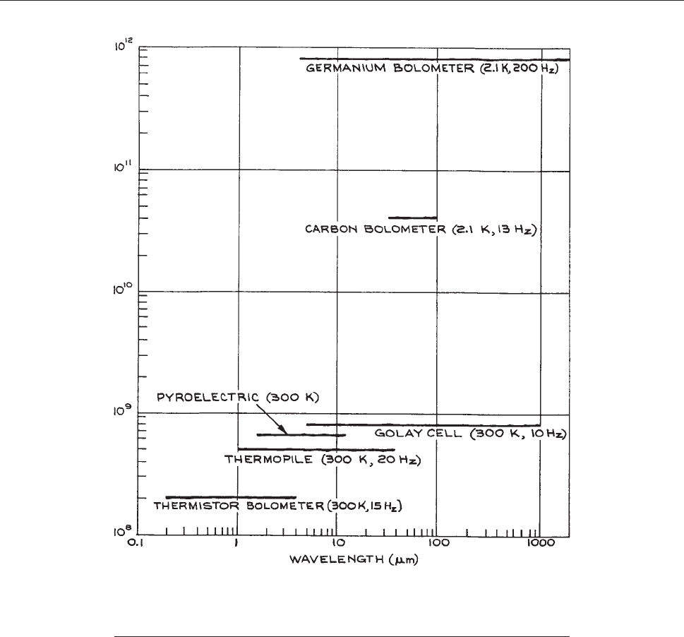
upward, as shown in Figu re 7.42. The absorbing
properties of the ‘‘black’’ su rface of t he detector will,
however, show some wavelength dependence, and the
necessity for a protective window on some detecto r
eleme nts may limit the useful spectral bandwidth of the
device. Most commonly available thermal detectors,
although by no means as sen sitive as various types of
photon detectors, a chieve spectral respons e very far
into the infrared – to the microwave region, in fact –
while con v eniently operating at room temperature. The oper-
ating characteristics of some commercially available thermal
detectors are given in Table 7.6. Each of these detectors is
d
iscussedbrieflybelow.Putley
55
giv es a more detailed
discussion.
Figure 7.42 Typical D
*
(k) curves for various thermal detectors assuming total
absorption of incident radiation. The operating temperature, modulation frequency,
and typical useful wavelength range are shown for each detector. In each case, the
detector is assumed to a view a hemispherical surround at a temperature of 300 K.
592 DETECTORS

7.10.1 Thermopiles
Thermopiles, although they are one of the earl iest forms
of infrared detector, are still widely used. Their operation
is based on the Seebeck effect, where heat ing the junc-
tion between two dissimilar conductors generates a
potential difference across the junction. An ideal device
should have a large Seebe ck coefficient, low resistance
(to minimize ohmic heating), and a low thermal conduc-
tivity (to minimize heat loss between the hot and cold
junctions of the thermopile). These devices are usually
operated with a n equal number of hot (irradiated) a nd
cold (dar k) junctions, the l atter serving as a ref erence
to compensate for d rifts in ambient temperature. Both
metal (copper–constantan, bismuth–silver, antimony–
bismuth) an d sem iconduct or ju nctions are used as the
active elements. The junctions can take the form of
evaporated films, which improves the robustness of the
devices and reduces their time constant, although this is
still slow (0.1 ms at best). Because a thermopile has very
low outpu t impeda nce, and generates low voltages, it
must be used with a specially designed low-noise ampli-
fier, or with a step-up transformer, as shown in Figure
7.
43. Such transformers can be conveniently built in the
labo
ratory by winding the primary and secondary coils
on a small ferrite torus.
Although thermopiles, along with other thermal detec-
tors, do not have absolutely flat spectral response over
unlimited wavelength regions, they can be remarkably flat
within restricted regions – in the visible or from 1 to 10
lm, for example. In addition, such detectors with calibra-
tions traceable to NIST are available. Thus they are invalu-
able in the absolute calibration (both for radiant sensitivity
and for spectral response) of light sources, detectors, and
spectrometers. Thermopiles are available from Boston
Electronics, The Eppley Laboratory, Hamamatsu, Laser Probe,
Perkin–Elmer Optoelectronics, Scientech, and Thorlabs.
7.10.2 Pyroelectric Detectors
Pyroelectric detectors utilize the change in surface charge
that results when certain asymmetric crystals (ones that can
possess an internal electric dipole moment) are heated. The
crystalline material is fabricated as the dielectric in a small
capacitor, and the change in charge is measured when the
element is irradiated. Thus, these devices are inherently a.c.
Table 7.6 Characteristics of commercially available thermal detectors
Device D
*
(cm Hz
1/2
W
1
) Time Constant Suppliers
Thermopile (1–4) 3 10
8
20 ls–60 ms Boston Electronics, Eppley Hamamatsu,
Laser Probe, Newport,
Perkin–Elmer Optoelectronics–Scientech, Thorlabs
Pyroelectric 10
6
–10
9
>100 ps Perkin–Elmer Optoelectronics, Hamamatsu,
Scientech Laser Probe, SensArray, Spiricon,
Scitec Instruments
Bolometer 2.5–10
8
1 ms Eltec Eltec, Electro-Optical Components
QMC Instruments SensArray Sofrdir
Golay Cell <10
10
NEP (W Hz
1/2
) ’10 ms QMC Instruments, Microtech Instruments
Figure 7.43 Operating circuit for a thermopile
using a dark junction (or junctions) and a differential
amplifier for compensation.
THERMAL DETECTORS 593
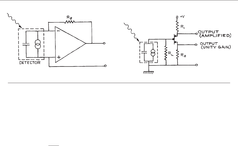
detectors. If the chopping frequency of the input radiation
is slow compared to the thermal relaxation time of the
crystal, the crystal remains close to thermal equilibrium
and the current response is small. When the chopping
period becomes shorter than the thermal relaxation time,
much greater heating and current response results. The
responsivity of the detector in this case can be written as:
R ¼
pðTÞ
qC
p
d
ðA=WÞð7:53Þ
where p(T) is the pyroelectric coefficient at temperature T,
d is the spacing of the capacitor electrodes, and q and C
p
are the density and specific heat of the crystal, respectively.
The equivalent circuit of a pyroelectric detector is a
current source in parallel with a capacitance, which can
range from a few to several hundred picofarads. For opti-
mum performance, the resultant high impedance must be
matched to a low-input-impedance, low-output-impedance
amplifier. Two examples of such circuits are given in
Figure 7.44. Pyroelectric detectors are available from
DIAS
Infrared GmbH, Hamamatsu, Laser Probe, Perkin–
Elmer Optoelectronics, Scientech, Scitec Instruments, and
SensArray.
Frequently pyroelectric detector packages contain two
pyroelectric elements connected with reverse polarity so
that the detector only responds to the difference in illumi-
nation between the two elements. This is a useful way to
reduce the effect of background radiation. For faster
response the capacitance of the detector must be shunted
with a small resistor (though this reduces the detectivity).
Pyroelectric detectors are robust and have frequency
responses extending from a few hertz to 100 GHz or so.
Their detectivities are comparable with those of thermo-
piles, and they also have a flat spectral response. They can
replace the thermopile in many applications as a conven-
ient, room temperature, wide-spectral-sensitivity detector
of infrared and visible light. Pyroelectric detector arrays
are available from Electro-Optical Components, Scitec,
SensArray, Spectum Detector, and Spiricon.
Pyroelectric detectors are widely used for the detection
of very short-duration infrared laser pulses. High-energy
pulses, however, generate acoustic waves in the detector
crystal giving rise to spurious signals. These acoustic sig-
nals are more of a problem in the observation of long laser
pulses (> 100 ns) than they are with short pulses. Pyro-
electric detectors are much more sensitive than photon-
drag detectors
56
for this purpose.
Photon-drag detectors operate by utilizing the momen-
tum transfer between photons and photo-produced carriers
in a material, creating an electromotive force. They are
fast, but relatively insensitive with typical NEP of 4 3
10
–3
WHz
1/2
. They are mainly used for detecting intense
pulses from 10 lm carbon dioxide lasers.
7.10.3 Bolometers
The resistance of a solid changes with temperature accord-
ing to a relation of the form:
RTðÞ¼R
0
1 þ c T T
0
ðÞ½ð7: 54Þ
Figure 7.44 Two examples of operating circuits for pyroelectric detectors.
594 DETECTORS
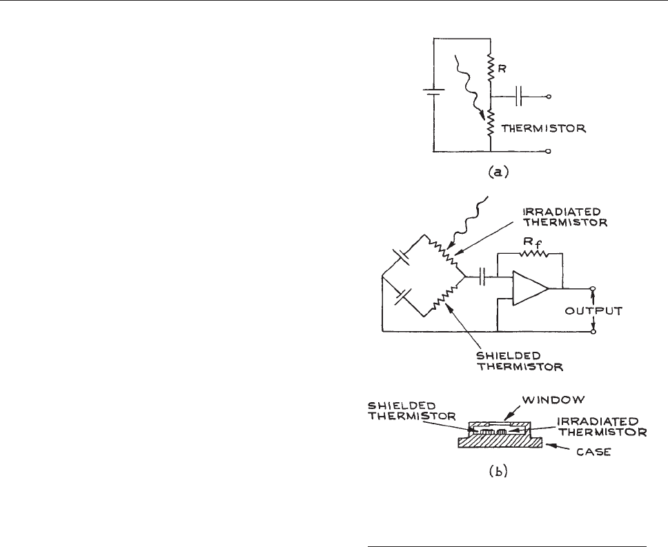
where c is the temperature coefficient of resistance, typi-
cally about 0.05/K for a metal, and R
0
is the resistance
at temperature T
0
.
A bolometer is constructed from a material with a large
temperature coefficient of resistance. Absorbed radiation
heats the bolometer element and changes its resistance.
Bolometers utilize metal, semiconductor, or almost super-
conducting elements. Metal bolometers utilize fine wires
(platinum or nickel) or metal films. The mass of the
element must be kept small in order to maximize its temper-
ature rise. Even so, the response time is fairly long (> 1 ms).
Semiconductor bolometer elements (thermistors) have
larger absolute values of c and have largely replaced metals
except where very long-term stability is required.
Bolometer elements can be operated in several ways; a
simple bias circuit for a single element is shown in Figure
7.45(a). However, it is usual to operate the elements in
pairs
in a bridge circuit, as shown in Figure 7.45(b) (see
also Chapter 6). One element is irradiated, while the sec-
ond
serves as a reference and compensates for changes in
ambient temperature.
Thermistors have a negative I–V characteristic above a
certain current and will exhibit destructive thermal run-
away unless operated with a bias resistor. It is usually best
to operate the thermistor at currents below the negative-
resistance part of its I–V characteristic. Bolometers can
operate to wavelengths up to 1000 lm, usually limited
by the transmission of their entrance window. These devi-
ces are available from B.F. Goodrich (acquired Barnes
Engineering from the EDO Corporation), Infrared Labo-
ratories, and Sofradir.
Microbolometers, generally used in thermal imaging
applications in the 8–16 lm spectral region, use a grid of
vanadium oxide or amorphous silicon on top of a silicon
grid. Infrared radiation heats the vanadium oxide, or amor-
phous silicon, and changes its electrical resistance. The
array of resistance changes is read out and provides a
thermal image of an object. They operate at room temper-
ature and do not require cooling.
Microbolometer arrays are typically 640 3 480, 320 3
240, or 160 3 120 pixels. Arrays are available from
NEC, Honeywell, and ULIS-IR. Complete camera systems
are available from BAE, CDIP, FLIR, Fluke Test Instru-
ments, Infrared Solutions, InfraredVision Technologies
Corporation (L-3 Communications), ISG Thermal Sys-
tems, Jenoptik, Land Infrared, Raytek, and Thermoteknix.
7.10.4 The Golay Cell
In a Golay cell (named for its Inventor, M.J.E. Golay),
57
radiation is absorbed by a metal film that forms one side
of a small sealed chamber containing xenon (used
because of its low thermal conductivity). Another wall
of the chamber is a flexible membrane, which moves
as the xenon is heated. The motion of the membrane
Figure 7.45 Operating circuits for thermistor
bolometers: (a) simple bias circuit; (b) bridge
circuit using compensating shielded thermistor,
with device construction shown.
THERMAL DETECTORS 595
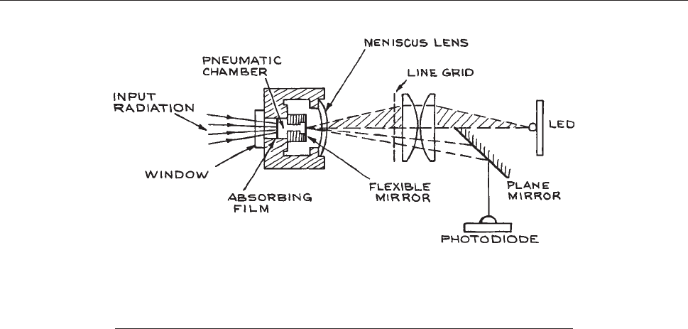
is used to change the amount of light reflected to a photo-
detector. The operating principle and essential design
features of a modern Golay cell are shown in Figur e
7.
46. Although these detectors are fragile, they are quite
sensiti
ve and are still used for far-infrared spectroscopy.
Golay cells are available from QMC Instruments and
Microtech Instruments.
7.11 ELECTRONICS TO BE USED
WITH DETECTORS
The primary signal from a photodetector may be a time-
varying current, as, for example, in the case of a photo-
multiplier, or a time-varying voltage, as, for example, in
the case o f a photodiode us ed in photovoltaic mode. In
general, the primary signal from the photodetector will be
proce ssed using electronics that follows the detector. This
is most often a current or voltage amplifier, or a current to
voltage converter (transimpedance) amplifier. When a
detector is being selected, it is often time-saving to buy
a detect or–amplifier integrated combination that
will provide a n electrical signal in a useful format fo r
analysis. Manufacturers’ data sheets should be consulted
for recommend ed operational circuits. A few issues are
important in designing or specifying circuits to be used in
conjunction with the detector. For optimum power trans-
fer, the output impedance of the detector should be
matched to th e input impedance of the followi ng circuit.
For example, if a photomultiplier is used with a 50 X
anode resistor, th en the input impedance of the following
circuitry should also be 50 ohm for optimum high-speed
perfo rmance. Ma ny volta ge amplifiers have a very large
input impedance, so if the input to the amplifier is con-
nected to a detector with output impeda nce R, the input
impedance of the circuit will become R. For high -speed
detector operation the signal from the detector may be
connected by 50 X coaxial cable to the input of the fol-
lowing electronics. The input impedance of these elec-
tronics should also be 50 X. The choice of input and
output impedance will a ffect the noise of the entire detec-
tor/amplifier combination. If the no ise figure of the elec-
tronics is known, then the overall noise performance can
be determined, using the methods discussed in Section
7.
8. If the detector/electronics combination has an
u
nknown noise figure then this will have to be determined
experimentally. This is a specialized endeavor, but many
manufacturers, such as Agilent, Maxim, National Instru-
ments, and Rohde and Schwarz have application notes
available to explain h ow thi s is done.
Figure 7.46 Schematic design of the Golay detector. The top half of the line grid is
illuminated by the LED and imaged back on the lower half of the grid by the flexible
mirror and meniscus lens. Any radiation-induced deformation of the flexible
mirror moves the image of the line grid and changes the illumination reaching the
photodiode.
596 DETECTORS
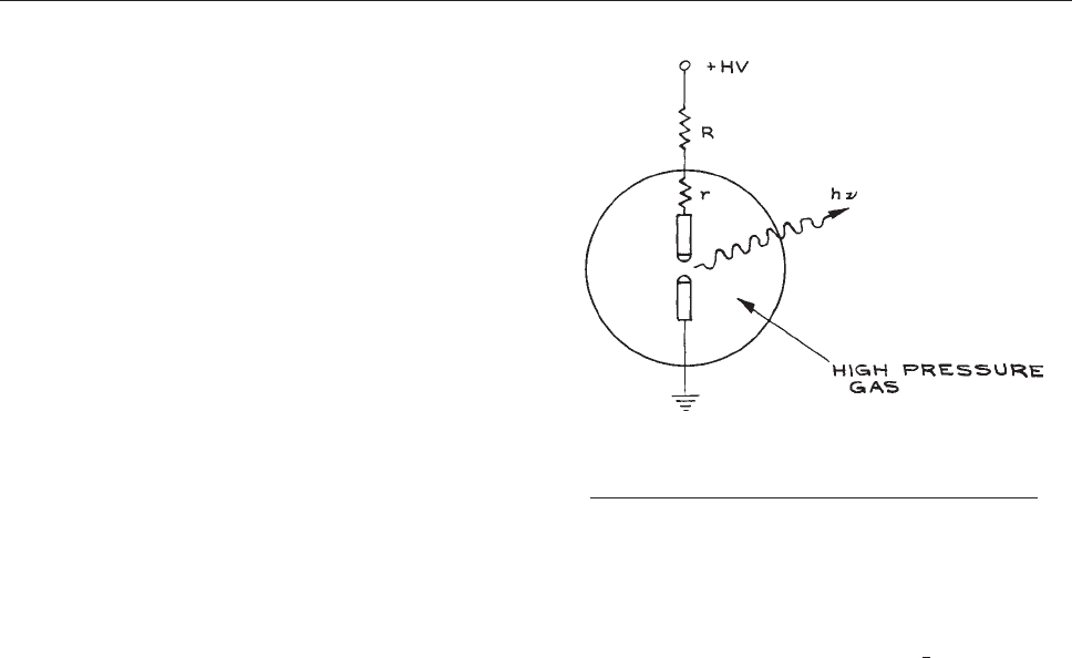
7.12 DETECTOR CALIBRATION
In certain cases, the data supplied by a detector manufacturer
on parameters such as D
*
(k)ors will only indicate a range of
values within which the detector’s characteristics will fall, or
the data may not be sufficiently reliable. If necessary, more
accurate detector calibration can be carried out.
To determine D
*
(k) for a detector, its response must be
measured with a source giving a known irradiance E
e
(k)
at the detector. This can be done either with a calibrated
source such as a blackbody, or by comparison with another
detector , such as a thermopile, which has a calibrated
response. To determine the temporal response function of
a detector operated in a giv en configuration, all that is nec-
essary is to irradiate the detector with a very short light pulse
and record the output pulse shape on a fast oscilloscope that
has its input appropriately terminated. For response func-
tions below about 1 ns, a sampling oscilloscope should
be used in conjunction with repetiti ve short-light-pulse irra-
diation of the detector . For detectors with response faster
than about 1 ns, suffi ciently short light pulses can be
obtained from a mode-locked Nd:YAG, Nd:glass, ruby, or
dye laser. Pulses from mode-locked argon or CO
2
lasers may
not be short enough to calibrate a very fast detector . To obtain
short light pulses outside con v eniently available wav elength
regions, nonlinear harmonic generation or mixing schemes
can be used, but the dif fi cultie s of such techniques can be
sev ere. To determine the time response of a detector that
responds slo wer than 1–2 ns, any pulsed light source of much
shorter duration than the detector response can be used.
Short-duration ( ’ 10 ns) flashlamps are available from
Perkin–Elmer Optoelectronics and Xenon Corporation.
Very-short-duration, low-energy, pulsed light sources
are easily made in the laboratory. A very simple design
is shown in Figure 7.47. A high-voltage discharge between
two
electrodes spaced by a few millimeters or less in a
high-pressure gas is used. Hydrogen works very well,
and even air at atmospheric pressure is satisfactory. To
obtain a short-duration flash, only the self-capacitance C
s
of the electrodes must be allowed to discharge. To accom-
plish this, a small charging resistor must be placed very
close to the high-voltage electrode; a larger series charging
resistor can be placed farther from the electrode. The tips
from ballpoint pens make excellent electrodes in this
application. The flash duration is proportional to L/p,
where L is the electrode spacing and p the gas pressure.
The breakdown voltage is proportional to L and also
approximately to p: the capacitance of the electrode gap
is proportional to L, so the flash energy
1
2
C
s
V
2
is propor-
tional to L
3
p
2
. Thus, for short-duration, high-energy
flashes, p should be high. The repetition frequency of the
lamp, which is most easily operated in a free-running
mode, will depend on the charging time constant.
Endnotes
a
The first dynode often has a larger d value than the others, but
we will assume that d is an average value.
b
The secondary ionization coefficient is the number of secondary
electron–hole pairs produced per unit length by a specific charge
carrier (electron or hole) in trav eling through the material.
Cited References
1 R. K. Bock and A. Vasilescu, The Particle Detector
Briefbook, Springer, New York, 1998.
2 C. Enss, Cryogenic Particle Detection, Topics in Applied
Physics, Vol. 99, Springer, New York, 2005.
3 R. C. Fernow Introduction To Experimental Particle
Physics, Cambridge University Press, Cambridge, 1989.
Figure 7.47 Simple design for high-pressure,
nanosecond-duration pulsed light source. Generally
R >> r, where r ranges from 1 k ohm to 1 M ohm.
DETECTOR CALIBRATION 597

4 K. Kleinknecht Detectors For Particle Radiation, 2nd
revised edn., Cambridge University Press, Cambridge, 1998.
5 P. W. Kruse, L. D. McGlauchlin, and R. B. McQuistan,
Elements of Infrared Technology, John Wiley & Sons, Inc.,
New York, 1962.
6 C. C. Davis, Lasers and Electro-Optics, Cambridge
University Press, Cambridge, 1996.
7 R. D. Hudson, Jr., and J. W. Hudson (Eds.), Infrared
Detectors, Benchmark Papers in Optics, Vol. 2, Dowden,
Hutchinson and Ross, Stroudsburg, PA, 1975.
8 D. Wood, Optoelectronic Semiconductor Devices, Prentice-
Hall, New York, 1994.
9 R. J. Keyes (ed.), Optical and Infrared Detectors, Topics in
Applied Physics, Vol. 19 Springer, Berlin, 1977.
10 R. H. Kingston, Detection of Optical and Infrared
Radiation, Springer Series in Optical Sciences, Vol. 10,
Springer, Berlin, 1978.
11 D. Attwood, Soft X-Rays and Extreme Ultraviolet Radiation
Principles and Applications, Cambridge University Press,
Cambridge, 2007.
12 P. Capper and C. T. Elliott (Eds.), Infrared Detectors and
Emitters: Materials and Devices, Kluwer, Dordrecht,
2001.
13 M. Henini and M. Razeghi (Eds.), Handbook of Infra-red
Detection Technologies, Elsevier, Amsterdam, 2002.
14 G. Knoll, Radiation Detection and Measurement, 3rd
revised edn., John Wiley & Sons, Ltd, Chichester, 2000.
15 G. H. Rieke, Detection of Light: From the Ultraviolet to the
Submillimeter, 2nd edn., Cambridge University Press,
Cambridge, 2003.
16 J. D. Vincent, Fundamentals of Infrared Detector Operation
and Testing, Wiley-Interscience, New York, 1989.
17 RCA photomultiplier tube types formerly manufactured by
RCA are supplied by Burle Industries (now merged with
Photonis).
18 Phillips photomultipler tubes were formerly available from
Amperex, but many of these tube types are now
manufactured by Photonis. These tubes are also available
from Richardson Electronics.
19 L. Brocco, D. Casadei, G. Castellini, et al., Behavior in
strong magnetic field of the photomultiplers for the
TOF system of the AMS-02 space experiment, Proceedings
of ICRC 2001: 2193, Copernicus Gesellschaft, 2001.
20 Static crossed-field photomultipliers used to be available
from ITT. See also V. J. Koester, Improved timing resolution
in time-correlated photon-counting with a static crossed-
field photomultiplier, Anal. Chem., 51, 458–459, 1979.
21 I. Prochazka, A. L. Migdall, A. Pauchard, et al. (Eds.),
Photon Counting Applications, Quantum Optics, and
Quantum Cryptography, Proceedings of SPIE – 6583, May
10, 2007.
22 H. R. Zwicker, in Optical and Infrared Detectors,R.S.
Keyes (Ed.), Topics in Applied Physics, Vol. 19, Springer,
Berlin, 1977, 149–196.
23 Photomultiplier Tubes: Basics and Applications
, 2nd edn.,
Hamamatsu
Photonics, Hamamatsu City, Japan, 1999.
24 ‘‘Window’’ discriminators are available from EG&G and
LeCroy.
25 Laser Focus Buyers Guide, published annually by Pennwell
Publishing Co., 1421 South Sheridan, Tulsa, OK 74112
01460, lists a large number of suppliers of a wide range of
optical detectors as does the The Photonics Buyers’ Guide,
published annually by Photonics Spectra, Laurin Publishing
Co., Berkshire Common, P.O. Box 4949, Pittsfield, MA
01202–4949.
26 D. Long, in Optical and Infrared Detectors, R. J. Keyes
(Ed.), Topics in Applied Physics, Vol. 19, 101–147,
Springer, Berlin, 1977.
27 W. J. Moore and H. Shenker , Infrared Phys., 5, 99–106, 1965.
28 F. J. Low, J. Opt. Soc. Am., 51, 1300–1304, 1961. See also
B. T. Draine and A. J. Sievers, High responsivity, low-noise
germanium bolometer for far infrared, Opt. Commun., 16,
425–429, 1976.
29 H. Shenker, W. J. Moore, and E. M. Swiggard, J. Appl.
Phys., 35, 2965–2970, 1964.
30 E. H. Putley, Appl. Opt., 4, 649–656, 1965.
31 M. A. C. S. Brown and M. F. Kimmitt, Infrared Phys., 5, 93–
97, 1965.
32 P. Norton, Opto-Elect. Rev., 10(3), 159–174, 2002.
33 G. L. Hansen, J. L. Schmit, and T. N. Casselman, J. Appl.
Phys., 53, 7099–7101, 1982.
34 J. Gowar, Optical Communication Systems, 2nd edn.,
Prentice-Hall, Englewood Cliffs, NJ, 1993.
35 H. Dautet, P. Deschamps, B. Dion, et al., Appl. Opt., 32(21),
3894–3900, 1993.
36 S. Cova, A. Lacaita, F . Zappa, and P. Lovati, in Advances in
Fluorescence Sensing Technology II, J. Lakowicz (Ed.),
Proc. SPIE 2388, paper 09, SPIE Conf. Photonics West, San
Jose, CA, USA, Feb. 6–7, 56–66, 1995.
37 A. Lacaita, F. Zappa, S. Cov a, and P. Lov ati, App. Opt., 35,
2986–2996, 1996.
38 S. Cova, M. Ghioni, A. Lacaita, C. Samori, and
F. Zappa, Appl. Opt. 35, 1956–1976, 1996.
39 T. Nesheim, Single photon detection using avalanche
photodiode, M.Sc. Thesis, Norwegian University of Science
and Technology, Trondheim, Norway, 1999.
40 H. J. Woltring, IEEE Transactions on Electron Devices,
22
(8), 581–590, 1975.
598 DETECTORS

41 A. J. Theuwissen (Ed.), Solid-State Imaging with Charge-
Coupled Devices (Solid-State Science and Technology
Library), Kluwer, Dordrecht, 2002.
42 T. V. Wilson, K. Nice, and G. Gurevich, How digital
cameras work. November 29, 2006 http://www.
howstuffworks.com/digital-camera.htm (June 02, 2007).
43 T. Klinger, Image Processing with Lab VIEW and IMAQ
Vision, Prentice-Hall, Englewood Cliffs, NJ, 2003.
44 R. J. McIntyre, IEEE Trans. Electr on. Devices, ED-13, 164–
169, 1966.
45 Hamamatsu Photon Counting Application Note. http://
sales.hamamatsu.com/assets/applications/ETD/
PhotonCounting_TPHO9001E04.pdf
46 C. C. Davis and T. A. King, J. Phys. A. 3, 101–109,
1970.
47 J. Milman and H. Taub, Pulse, Digital, and Switching
Waveforms, Chap. 3, McGraw-Hill, New York, 1965;
C. N. Winningstad, IRE Trans. Nucl. Sci, NS43, 26, 1959;
C. L. Ruthroff, Proc IRE, 47, 1337, 1959.
48 L. J. Richter and W. Ho, Rev. Sci. Instrum., 57, 1469, 1986;
R. M. Tromp, M. Copel, M. C. Reuter, Rev. Sci. Instrum., 62,
2679, 1991.
49 P. Horowitz and W. Hill, The Art of Electronics, 2nd edn.,
Cambridge Universtiy Press, Cambridge, 1989.
50 V. Radeka, in Annual Review of Nuclear and Particle
Science, Vol. 38, J. D. Jackson (Ed.), 1988, pp. 217–278.
51 R. L. Heath, R. Hofstadter and E. B. Hughes, Nucl. Instr.
Meth., 162, 431–476, 1979.
52 J. B. Birks, Theory and Practice of Scintillation Counting,
Pergamon Press, New York, 1964.
53 R. K. Bock and A. Vasilescu, The Particle Detector
Briefbook, Springer, Berlin, 1998.
54 G. Knoll, Radiation Detection and Measurement, 3rd
revised edn., John Wiley & Sons, Ltd, Chichester, 2000.
55 E. H. Putley, in Optical and Infrared Detectors, R. J. Keyes
(Ed.), Topics in Applied Physics, Vol. 19, Springer, Berlin,
1977.
56 A. F. Gibson, M. F. Kimmitt, and A. C Walker, Appl.
Phys. Lett., 17, 75–77, 1970. See also R. Kesselring, A. W.
Kalin, and F. K. Kneubuhl, Infrared Phys., 33, 423–436,
1992.
57 M. J. E. Golay, Rev. Sci. Instrum., 18, 357–362, 1947.
General References
D. Attwood, Soft X-Rays and Extreme Ultraviolet Radiation
Principles and Applications, Cambridge University Press,
Cambridge, 2007.
R. K. Bock and A. Vasilescu, The Particle Detector Briefbook,
Springer, Berlin, 1998.
P. Capper and C. T. Elliott (Eds.), Infrared Detectors and
Emitters: Materials and Devices, Kluwer, Dordrecht, 2001.
C. C. Davis, Lasers and Electro-Optics, Cambridge University
Press, Cambridge, 1996.
C. F. G. Delaney and E. C. Finch, Radiation Detectors, Oxford
Science Publications, Clarendon Press, Oxford, 1992.
C. Enss, Cryogenic Particle Detection, Topics in Applied
Physics, Vol. 99, Springer, Berlin, 2005.
R. C. Fernow, Introduction To Experimental Particle Physics,
Cambridge University Press, Cambridge, 1989.
M. Henini and M. Razeghi (Eds.), Handbook of Infra-Red
Detection Technologies, Elsevier, Amsterdam, 2002.
R. D. Hudson, Jr., and J. W. Hudson (Eds.), Infrared Detectors,
Benchmark Papers in Optics, Vol. 2, Dowden, Hutchinson and
Ross, Stroudsburg, PA, 1975.
K. Kleinknecht, Detectors For Particle Radiation 2nd revised
edn., Cambridge University Press, Cambridge, 1998.
R. H. Kingston, Detection of Optical and Infrared Radiation,
Springer Series in Optical Sciences, Vol. 10, Springer , Berlin,
1978.
G. Knoll, Radiation Detection and Measurement, 3rd revised
edn., John Wiley & Sons, Inc., New York, 2000.
P. W. Kruse, L. D. McGlauchlin, and R. B. McQuistan, Elements
of Infrared Technology , John W iley & Sons, Inc., New York,
1962.
R. J. Keyes (Ed.), Topics in Applied Physics, Optical and
Infrared Detectors, Springer, Berlin, 1977.
G. H. Rieke, Detection of Light: From the Ultraviolet to the
Submillimeter, 2nd edn., Cambridge University Press,
Cambridge, 2003.
J. D. Vincent, Fundamentals of Infrared Detector Operation and
Testing, Wiley-Interscience, New York, 1989.
D. Wood, Optoelectronic Semiconductor Devices, Prentice-Hall,
New York, 1994.
REFERENCES 599

MEASUREMENT AND CONTROL OF TEMPERATURE
*
There are two levels of concern with temperature in
scientific experiments. One is the control of temperature
to achieve some secondary (but essential) aim in the appa-
ratus. Examples are the use of a cold trap in a vacuum line,
and the use of heaters and coolants in a distillation column.
For such needs, the temperature needs only to be known
and kept constant to within a few kelvins. In the second
case, the measurement of the dependence of physical
parameters on temperature is a primary aim of the experi-
ment. A physicist learns about the nature of a material by
measuring such properties as density or heat capacity as a
function of temperature. An organic chemist studies the
kinetics of a chemical reaction by measuring its rate of
reaction as a function of temperature. For these experi-
ments, the temperature must be varied over a range and
controlled at any point in that range, at resolutions better
than 1 K.
Sometimes the temperature must be known accurately.
That is, the measurement must be closely calibrated to the
International Temperature Scale. Accurate measurements
are necessary if the new data are to be used with other
measurements on the system under study. If measurements
of the density of water are to be combined with measure-
ments of its kinematic viscosity to calculate its shear vis-
cosity as a function of temperature, then the temperature
must be measured with the same accuracy in both the
density measurements and the kinematic viscosity meas-
urements. The accuracy also matters if measurements in
one laboratory are to be compared to measurements in
another laboratory of that same quantity (e.g., the shear
viscosity as a function of temperature).
For some purposes, the precision is more important than
the accuracy. Such is the case when it is the derivative of a
property with respect to temperature that is of interest.
Then the changes in temperature need to be measured with
very fine resolution, but the accuracy, the exact temper-
ature on the international scale, is not as important. A
physicist wishing to test a theoretical prediction for the
thermal expansion (the change of volume with tempera-
ture) of a superconducting solid will be more concerned
with precision than with accuracy, even though he or she
will have some requirements on the accuracy.
In this chapter we will describe how to measure and
control the temperature for simple needs, usually meaning
a resolution of 1 K. We will also describe more precise and
accurate methods for temperature measurement and control,
methods that achieve a resolution of 1 mK and better. Since
we must be able to measure the temperature in order to
control it, we will first discuss thermometry. For both meas-
urement and control, we will focus on the temperature range
from 10 K to about 1800 K, and on methods that are prac-
tical for most laboratories. We will briefly discuss thermom-
etry at very low and very high temperatures.
8.1 THE MEASUREMENT OF
TEMPERATURE
A thermometer can be constructed from a system with a
measurable property that depends strongly on temperature.
We will discuss here the ‘‘working’’ thermometers useful
*
By Sandra C. Greer, The University of Maryland, College Park, MD
and Mills College, Oakland, CA.
600
CHAPTER
8
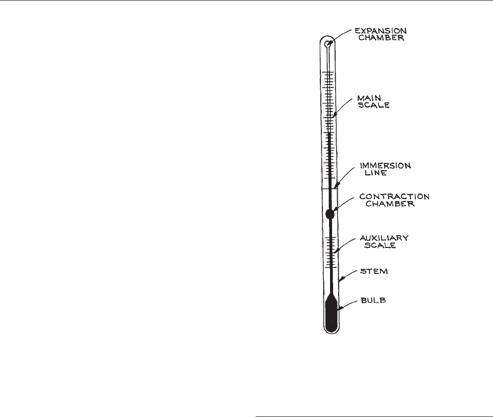
in most laboratories, as opposed to special ‘‘standard’’
thermometers, such as gas thermometers, used in calibra-
tion laboratories.
1–4
8.1.1 Expansion Thermometers
Expansion thermometers use as the thermometric property
the volume of the thermometric system. For example, the
common mercury thermometer uses the change in volume
(as reflected in the change in length) of a column of mer-
cury confined to a cylindrical capillary tube. There exist
expansion thermometers using the thermal expansion of a
metal that have industrial applications.
2
We will limit our-
selves to the liquid-in-glass thermometers used in scien-
tific research.
5,6
Liquid-in-glass thermometers date to the
seventeenth century
1
and are still common in research lab-
oratories. They do not lend themselves readily to computer
automation of the measurement process, but they are use-
ful for approximate measurements that do not need to be
automated, or as laboratory standards for the calibration of
other thermometers.
Such thermometers are limited in range by the freezing
and boiling points of the liquids used and by the softening
point of the glass in which the liquid is contained. Mercury
has been the most common thermometer fluid because of
its nearly linear coefficient of thermal expansion, but
organic liquids are also used and are safer. Design consid-
erations also include the choice of the glass and the relative
dimensions of the parts of the thermometer. Thermometers
can be designed for high sensitivity in a particular range by
including in the liquid column a section of larger diameter,
a contraction chamber, so that the liquid expands in that
volume before it reaches the range of interest (see Figure
8.1). Mercury thermometers can operate in the range 235–
923
K. Organic liquids have the disadvantages that they do
not have very linear thermal expansions and they must be
dyed to be visible, but they are still useful: toluene (183 to
373 K), ethanol (163 to 373 K), pentane (73 to 293 K).
Thermometers made with mercury and with organic
liquids are available with resolutions as good as 0.02 K
(Brooklyn Thermometer).
There are a number of difficulties in obtaining high
accuracy and precision with liquid-in-glass thermometers.
Good thermal contact between the thermometer and the
system of interest is difficult to achieve for systems other
than fluids. The thermometer can be sensitive to pressure
changes. If the thermometer is heated to its highest temper-
atures, it will require days to return to its original calibra-
tion because of hysteresis in the glass.
Mercury thermometers designed to be accurate and sta-
ble to about 0.01 K over temperature ranges of 3 to 5 K are
commercially available (Brooklyn Thermometer, Omega
Engineering) and make good, cheap working temperature
standards. Mount the mercury thermometer in a stirred
bath, the temperature of which is under control (Section
8.2), along with any other thermometers that you want to
Figure 8.1 Mercury-in-glass thermometer. The auxiliary scale
is designed to allow calibration at the ice point. The contraction
chamber permits high sensitivity (a small capillary diameter)
without having a very long stem. The immersion line indicates
the depth to which the thermometer was immersed in the
calibration bath. The expansion chamber prevents the buildup
of pressure and avoids breakage on overheating.
MEASUREMENT OF TEMPERATURE 601MEASUREMENT OF TEMPERATURE 601
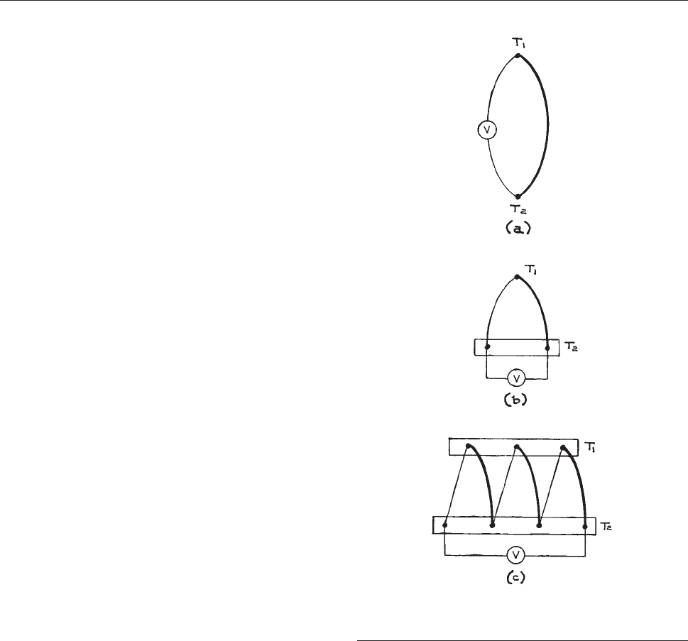
calibrate against the mercury thermometer. Be careful in
reading the meniscus position to avoid parallax error; a
telescope makes this easier. Use the thermometer at the
same immersion depth at which it was originally cali-
brated; a difference in immersion depth will necessitate
stem corrections. Tap the thermometer before each meas-
urement to avoid sticking of the mercury column to the
stem wall. Monitor the stability of the thermometer by
regularly measuring the ice point (Section 8.1.9).
A
final hint: if the liquid in a thermometer becomes
separated, it can be rejoined by cooling the thermometer
bulb with dry ice shavings until all the liquid is back in the
bulb. Never heat a liquid-in-glass thermometer to expand
the liquid to the full length of the capillary tube in an effort
to rejoin the liquid: the thermometer will break.
8.1.2 Thermocouples
7–10
Thermocouples use as the thermometric property the volt-
age that develops between two junctions of two different
metals when the junctions are at different temperatures.
11
Thermocouple thermometers have been used since about
1885,
12
and still have uses ranging from hand-held digital
thermometers to sophisticated calorimeters.
When there exists a difference in electron density
between two points in a metallic conductor, a voltage
develops between those two points. Such a difference in
electron density can arise even in a conductor made of a
homogeneous metal, because the electron density varies
when the temperature varies. Thus, a temperature gradient
across any metallic material causes a voltage to develop
across that material. If we try to measure this voltage by
attaching leads made of the same metal, then the voltage
difference will also develop in the leads and the effects will
cancel. If the leads are of a different metal, as shown in
Figure 8.2(a), then the difference in the thermally induced
vo
ltages between the two metals will cause a net voltage
between the junctions: the Seebeck effect.
13
This thermo-
electric voltage, or ‘‘thermal emf,’’ depends upon the par-
ticular choice of metals and upon the difference in
temperature between the junctions, but depends only
slightly on the pressure. The Seebeck effect is a bulk prop-
erty of metals in a temperature gradient. It is not a property
of the junctions themselves: it is not a ‘‘contact potential,’’
and treating it as such can lead to mistakes in the use of
thermocouples.
14
A related property is the Peltier effect:
15
when a current is passed through a circuit such as Figure
8.2(a), by replacing the voltmeter with a battery, then one
junction
will be heated and the other junction will be
cooled. The Peltier effect can be used to construct electri-
cal heating and cooling devices.
The connection of two wires of two different metals at
junctions at two different temperatures,asinFigure 8.2(a),
Figure 8.2 Thermocouple configurations. Lines of different
thicknesses represent wires of different metals or alloys. T
1
and T
2
are two different temperatures. V is a voltmeter.
602 MEASUREMENT AND CONTROL OF TEMPERATURE602 MEASUREMENT AND CONTROL OF TEMPERATURE

is called a thermocouple. The voltage developed across the
thermocouple is a measure of the difference in tempera-
ture, (T
1
– T
2
). Thus, the measurement of the temperature
with a thermocouple requires only a voltmeter of sufficient
resolution. The relationship between the thermoelectric
voltage and the temperature difference, while nearly a
direct proportionality, cannot be predicted, but must be
measured for a given pair of metals. The nature of the
Seebeck effect leads to several principles useful in the
design of such thermocouple thermometers:
2,16
(1) The law of homogeneous metals: a thermocouple
requires two different metals. If the two wires are of
the same material, then no net thermal voltage will
develop, even in the presence of a temperature gra-
dient. Therefore, voltmeter lead wires, as shown in
Figure 8.2(b), will not contribute to the measured volt-
age
if they are made of the same metal, and if their
ends (at T
2
and at the voltmeter) are at the same tem-
peratures so that they are under the same temperature
gradient. On the other hand, inhomogeneities due to
strains or impurities in a metal conductor will be, in
effect, regions of a different metal, and will, in the
presence of a temperature gradient, act as ‘‘mini-
thermocouples,’’ generating spurious thermal voltages
and leading to inaccuracies in the thermometry.
(2) The law of intermediate metals: a thermocouple
requires two different temperatures. If there is no dif-
ference in temperature between the ends of a pair of
wires, then no net thermal voltage will develop
between them, even if the wires are of different metals.
That is, in Figure 8.2(a),ifT
1
¼ T
2
, no voltage devel-
ops. A consequence of this law is that another wire
may be inserted into the thermocouple circuit, so long
as both ends of that wire are at a common temperature,
that need not be either of the temperatures involved in
the actual thermocouple (T
1
or T
2
). This means that
thermocouple junctions may be made with any kind of
solder or any other method of attachment, so long as
each junction is itself all at the same temperature.
(3) The law of successive metals: if thermocouples are
made of pairs of metal A with metal B, metal B with
metal C, and metal A with metal C, then the voltages
developed by each of the thermocouples between a
given pair of junction temperatures will be related as
V
AC
¼ V
AB
+ V
BC
. This equation allows the calculation
of tables of thermocouple voltages for any pair of
metals A and C if the tables are already available for
A and C with respect to a reference metal B.
(4) The law of successive temperatures: if a given thermo-
couple develops a voltage V
a
between T
1
and T
2
and a
voltage V
b
between T
2
and T
3
, then it will develop a
voltage V
c
¼ V
a
+ V
b
between T
1
and T
3
. It follows that
only the junction temperatures matter: intermediate
temperatures along homogeneous wires do not matter.
It also follows that if thermocouple tables are available
in which voltages are given for each temperature T
1
with respect to a reference temperature T
2
, then vol-
tages may be calculated with respect to a different
reference temperature T
3
if the voltage V
b
is known.
Thermocouple junctions may be placed in series in order
to amplify the voltage signal. Such a thermopile is shown
in Figure 8.2(c), where there are three identical thermo-
couples
in series, producing a voltage three times that of a
single thermocouple (since voltages in series add).
There are a great many possible thermocouple pairs,
since any two metals or alloys can form a thermocouple.
The choice of a particular pair will depend upon its sensi-
tivity in the temperature range of interest and upon such
considerations as corrosion resistance. Several thermocou-
ple pairs have come into common use; their properties are
well known, and good-quality wire is readily available
(Omega Engineering; Watlow).
Table 8.1 gives the most common thermocouple types
and
their properties. Types C, D, and G are all various
combinations of alloys of tungsten and rhenium, and are
useful at high temperatures because these metals do not
readily vaporize. Types R and S are of platinum with
platinum–rhodium alloy and have low sensitivity, but have
high stability and accuracy. Types K, N, and E all use
nickel alloys. Type K has a wide range of usefulness,
low thermal conductivity, and good resistance to oxidation,
but cannot be used in a reducing atmosphere above 1100 K
and shows instability in the calibration due to a phase
transition in Chromel at 570 K. Type N is a more stable
substitute for Type K. Type E is common in low-temperature
applications because the thermal conductivities of the
materials are low, and thus the wires do not carry
heat into the apparatus. Types E, J, and T all use the
MEASUREMENT OF TEMPERATURE 603MEASUREMENT OF TEMPERATURE 603

copper–nickel alloy Constantan. Type J has the advantage
of high sensitivity and the disadvantage that iron is readily
oxidized. Type T, probably used most often, has the advant-
age that one material is copper, from which the voltmeter
leads are also likely to be made, so that the chance of
extraneous thermal voltages is reduced. On the other hand,
copper oxidizes above 620 K and has a very high thermal
conductivity (see Table 8.5 below). The last two Chromel
th
ermocouples in Table 8.1, one with gold–iron alloy and
on
e with copper–iron alloy, are used at cryogenic temper-
atures, along with types E, K, and T (Section 8.1.5). Ther-
mo
couples made of wires from two different elemental
metals (gold, silver, platinum, etc.) can be used for cases
requiring very high stability and precision.
4,17
The construction of reliable thermocouple thermo-
meters requires care. Use good-quality, annealed thermo-
couple wire. Each wire can be individually tested for
homogeneity by connecting its ends to a voltmeter and
passing the wire slowly through liquid nitrogen; wires that
do not show any measurable thermoelectric voltage are
suitable for use. Use the largest-diameter wire that you
can tolerate: large wire is more likely to be homogeneous
and is less susceptible to strains. Make the junctions
mechanically sound and electrically and thermally contin-
uous. In principle, thermocouple wires can be twisted or
clamped to make a junction.
9
In practice, better results are
obtained if they are soldered or welded (see Section 1.4).
F
or work below 443 K, Type T can be joined with ordinary
tin–lead solder, using a rosin flux. All can be soldered with
low melting tin–silver solder. For work at higher temper-
atures and for better mechanical strength, all can be brazed
with a high-melting silver alloy (Section 1.4.6). All but
T
ype T can be spot-welded. All can be welded with a torch,
using a reducing flame of oxygen with either natural gas or
acetylene to melt the two wires together into a firm bead.
Ready-made thermocouples, thermopiles, and thermopile
arrays can be purchased from Omega Engineering,
SensArray, InstruLab, Watlow, et al.
Make good thermal contact between the junctions and
the points at which the temperatures are to be measured.
Junctions can be mechanically attached to solids using a
thermally conducting grease, or bonded with a thermally
conducting adhesive (Cotronics, Omega Engineering,
Wakefield). Thermocouples are often placed in protective
metal or ceramic sheaths (thermowells),
16
but such
arrangements increase the response time. Protect the wires
from mechanical stresses. The wires can be electrically
insulated with Teflon (to 553 K) or Kapton (to 700 K);
fiberglass or ceramic is required for higher temperatures.
Avoid air drafts and temperature gradients in the vicinity of
a thermocouple circuit.
A thermocouple or thermopile produces a low-level d.c.
voltage (10–100 lV) that requires particular care in meas-
urement (see Keithley handbook
18
and application notes).
A digital voltmeter of appropriate sensitivity suffices for
the measurement of the thermocouple voltage (Keithley,
Agilent). Follow appropriate procedures for shielding and
grounding in the measurement circuitry (Section 6.9).
Commercial
thermocouple amplifiers are available for $2
to $20 (Analog Devices, Linear Technology). Sometimes
(e.g., for control purposes) it is desirable to linearize the
output signal, and such circuits are also available (Analog
Devices).
Thermocouples measure the temperature differences
between junctions. This property can be used to advantage
Table 8.1 Properties of common thermocouples
Type
a
Materials Useful
Range
(K)
Sensitivity
(lVK
1
)
20 K 300 K
C, D, G Tungsten/Rhenium 32–2600 — 20
R, S Platinum/PtRh 220–1800 — 6
K Chromel
b
/Alumel
c
10–1500 4.1 41
N Nicrosil/Nisil
e
10–1500 3 26
E Chromel
b
/Constantan
d
10–700 8.5 61
J Iron/Constantan
d
60–1000 — 52
T Copper/Constantan
d
20–700 4.6 41
Chromel
b
/AuFe 10–1000 15 20
Chromel
b
/CuFe 10–300 >11
a
The type designation is that of the Instrument Society of
America
b
Chromel is an alloy of nickel with 10% chromium
c
Alumel is an alloy of nickel with 2% aluminum, 2%
manganese, and 1% silicon
d
Constantan is an alloy of copper with 43% nickel
e
Nicrosil is a alloy of nickel, chromium, and silicon; Nisil is an
alloy of nickel, magnesium, and silicon.
604 MEASUREMENT AND CONTROL OF TEMPERATURE604 MEASUREMENT AND CONTROL OF TEMPERATURE

when a difference is just what is required, as in some
temperature-control circuits. If, instead, an absolute tem-
perature measurement is required, then one junction (the
reference junction) must be kept at a constant, known tem-
perature. For example, let T
2
in Figure 8.2 be the reference
junction of known T
2
. Then the absolute temperature at T
1
is obtained by combining the known T
2
and the difference
(T
1
– T
2
) as obtained from the thermocouple voltage (see
below). A simple (but inconvenient) way to do this is to
keep the reference junction at 273.15 K by immersing it in
a slurry of ice and water (see Section 8.1.9). The reference
temperature can also be established with commercially
available fixed point cells that are made from Peltier devi-
ces (Hart Scientific, Omega Engineering; $1200).
Two less-expensive methods are either to make an iso-
thermal block, or to use an electronic compensation circuit.
An isothermal block consists of a material of high thermal
conductivity (Table 8.5) onto which the reference junction
and
an independent thermometer are mounted with good
thermal contact, and then surrounded by thermal insulation
(Table 8.5). Then the independent thermometer is used to
measure
the reference temperature. This is useful, even
though it requires an independent thermometer, because
that thermometer only needs to function near room temper-
ature, but then permits thermocouple measurements of
temperatures far from room temperature.
An electronic compensation circuit or ‘‘electronic ice
point’’ is an electronic circuit that measures the temper-
ature at the reference junction and then adds a voltage to
the thermocouple circuit that compensates for the fact that
the reference junction is not actually at 273.15 K. These
‘‘cold junction compensation’’ circuits can be made from
components, or purchased. Analog Devices and Linear
Technology make integrated circuits (AD594, AD595,
LT1025) that include both compensator and amplifier for
$15–$40, and Omega makes complete devices for $200–
$600. For the best thermocouple measurements of temper-
ature, reference junctions made from ice baths or other
fixed-point baths (Sections 8.1.9; 8.2.1) permit more accu-
rate
measurements (60.01 K) than do these isothermal
blocks and electronic ice points (60.4 to 61 K).
In order to convert the thermocouple voltage to a tem-
perature, it is n ecessary to use conversion table s or to
calibrate directly. The National Institute of Standards and
Technology has published extensive tables of thermo-
couple voltages. A calibration using the tables is likely
to be accurate only to a few degrees, due to variations
among wires. For more accurate measurements, the ther-
mocouple must be compared with a standard thermometer
(usually a platinum resistance thermometer; see Section
8.1
.3 below) over the temperature ran
ge of interest. Voltage-
temperature points either from the tables or from a direct
calibration can be fitted by a polynomial:
T ¼ a
0
þ a
1
V þ a
2
V
2
þ ð8:1 Þ
where T is the temperature, V is the voltage, and enough
terms are included to describe the data. The calibration
determines the accuracy of the temperature measurement
on the International Temperature Scale (Section 8.1.9). The
pr
ecision of temperature measurements with thermocouples
is considerably better than the accuracy: temperature differ-
ences can be resolved to 1 mK, using thermopiles and sen-
sitive amplifiers/voltmeters.
The advantages of thermocouples as thermometers are:
they are simple, rugged, and inexpensive; thermopiles can
have resolutions of 1 mK; they can be used over a very
broad range of temperature (see Table 8.1); they are small;
they
respond quickly. The disadvantages are: the voltage
signals are small and hard to measure; accuracy is hard to
attain and maintain; a reference junction is necessary for
absolute temperature measurements; they are very sensi-
tive to magnetic fields.
8.1.3 Resistance Thermometers
Resistance thermometers use as the thermometric property
the dependence of electrical resistance on temperature.
There are two main kinds of resistance temperature detec-
tors (RTDs): conducting metal RTDs and semiconductor
RTDs. Metal RTDs have been in use since the late nine-
teenth century,
19
whereas semiconductor RTDs came into
use only in the twentieth century. Resistance temperature
detectors are invaluable in modern thermometry because
they are small and stable, and provide an easily measured
electrical quantity.
Metal Resistance Thermometers.
6
Metal resist-
ance thermometers consist of wire coils or thin films of
electrically conducting metals or alloys, together with the
MEASUREMENT OF TEMPERATURE 605MEASUREMENT OF TEMPERATURE 605
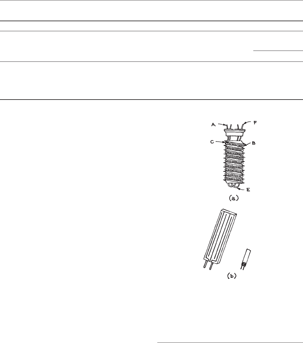
instrumentation needed to measure the electrical resist-
ance. As the temperature increases, the increase in kinetic
energy of the metal atoms leads to an increase in the elec-
trical resistivity. The larger the initial resistance, the larger
the change of resistance with temperature, and thus the
greater the sensitivity.
While a number of metals can be used for thermometry
(Table 8.2), platinum is most commonly used because it is
resistant
to corrosion and its electrical resistance has a
nearly linearly increase with temperature of 0.4%/K.
20
Indeed, the platinum resistance thermometer (PRT) is the
standard device for the International Temperature Scale of
1990 between 13.8033 K and 961.78 K (see Section
8.1.9).
21
Some typical platinum resistance thermometers
are shown in Figure 8.3. Usually, PRTs have resistances of
25
or 100 X at room temperature, but thin-film PRTs can
have resistances of 1000 to 2000 X. The resistance as a
function of temperature behaves as (see Figure 8.4):
R ¼ R
0
þ R
1
T þ R
2
T
2
þ ð8:2Þ
where the T
2
term is important for measurements with a
resolution of millikelvins. With care in the resistor construc-
tion and in the measurement circuitry, a resolution of 0.1 mK
can be achiev ed over a very broad range of temperatures
with platinum resistance thermometers (see Figure 8.4 and
Table 8.2), available from suppliers such as Barnant, Hart,
Lake
Shore Cryotronics, Minco, Omega Engineering, and
Table 8.2 Properties of common resistance thermometers
3
Materials Resistivity
(Xm) 3 10
8
at 273 K
Temperature Coefficient
of Resistance
(K
1
) 3 10
3
Useful Range (K) Sensitivity
a
(mK)
20 K 300 K
Platinum 11 3.9 20–1000 10 0.1
Nickel 59 6.0 213–423 — —
Copper 1.7 3.9 173–373 — —
Ruthenium oxide — — 0.04–40 5
c
—
Rhodium–iron
b
42
c
— 0.5–300 0.05 5
a
Approximate resolution under typical conditions.
b
Not for use in magnetic field.
c
At 4.2 K.
Figure 8.3 Platinum resistance thermometers: (a) standard,
high-resolution model made by Minco Products, Inc., in which
the platinum is wound as a wire coil on a ceramic base. Two
leads (A) pass through the lid and attach to one end of the coil
(B) at C. At the other end, two leads are again attached (E) and
pass through the center of the base to the lid at F. The
assembly is then enclosed in a inert atmosphere. This PRT is
3/8’’ long; (b) Film RTD such as those made by Omega
Engineering, Inc. They can be very small, 1/8’’ or less in length.
606 MEASUREMENT AND CONTROL OF TEMPERATURE606 MEASUREMENT AND CONTROL OF TEMPERATURE
Rosemount. Thin, surface-mount foil resistance thermome-
ters made from platinum are also available (Minco).
Resistance thermometers are also made of other metals
(see Table 8.2). Nickel has a high sensitivity to temperature
change,
but the dependence of resistance on temperature is
nonlinear, making its use over a large temperature range
more difficult.
22–24
Copper has a low resistivity, so a longer
wire is required to achieve a useful resistance, but its resist-
ance is fairly linear in temperature.
25,26
Copper and nickel
thermometers are made by Thermometrics. The other
materials in Table 8.2 are used for cryogenic thermometry
and
will be discussed below in Section 8.1.5. New materi-
als,
such as niobium thin films, are under development for
resistance thermometry.
27
Semiconductor Resistance Thermometers.
Thermistors
12,16
are small beads of semiconducting mate-
rial (metal oxides), the resistance of which depends on
temperature (Table 8.3). While electrons flow freely in a
metal,
in a semiconductor, the electrons must first be
excited into a conducting state; the electrons will thus flow
more freely and the resistance will decrease as the temper-
ature increases. The term ‘‘negative temperature coeffi-
cient’’ or ‘‘NTC’’ is used. The resistance of a thermistor
decreases at a rate of about 4%/K; a thermistor is 10 times
more sensitive than a PRT. A thermistor differs from a
metal resistance thermometer in that its electrical resist-
ance is much more sensitive to temperature change, its
resistance decreases as temperature increases, and its
resistance is not linear in its temperature dependence
(see Figure 8.4). There exist thermistors that have positive
temperature
coefficients of resistance, for which the resist-
ance increases with temperature as for metals; they are not
useful for thermometry, but are used for circuit protection
devices.
16
The Steinhart–Hart equation provides a good empirical
description for a thermistor (see Figure 8.4):
28,29
1=T ¼ A þ Bðln RÞþCðln RÞ
3
þ ð8:3Þ
where A, B,andC are empirical constants and where
higher-order terms of odd power may be required for a
broad temperature range or for high resolutio n. If a
linearized resistance is required, then linearizing cir-
cuits can be made
12,16
or bought. For example, t he YSI
Figure 8.4 The left ordinate gives the resistance as a function
of temperature T for a thermistor (solid line) which has a room
temperature resistance of about 4 kX, and for a platinum
resistance thermometer, PRT, (dotted line) which has a room
temperature resistance of about 100 X. Note that the scales
differ by a factor of 1000. The right ordinate gives the
thermoelectric voltage referenced to 273 K of a Type T
copper/constantan thermocouple (dashed line) as a function
of temperature.
Table 8.3 Properties of common semiconductor
thermometers
Type Materials Useful
Range
(K)
Sensitivity
a
(mK)
20 K 300 K
Semiconductor Thermistor 77–600 — 0.01
Germanium
b
1–30 0.5 —
Carbon 0.04–300 1 10
3
Carbon-in-glass 1–100 0.75 —
Diode Silicon
b
0.01–300 20 15
Gallium arsenide
b
0.01–300 15 100
a
Approximate resolution under typical conditions
b
Not for use in magnetic field
MEASUREMENT OF TEMPERATURE 607MEASUREMENT OF TEMPERATURE 607

model 4800 linearizes thermistor output to 60.1 K from
273 K to 373 K ($75). (YSI and Betatherm are now
subdivisions of Measurement Specialties.) L inearizing
circuits for thermistors are also available from O mega
Engineering.
Typical thermistor resistances are 1 to 10 kX. Thermis-
tors can readily resolve a millikelvin and can be made to
resolve a microkelvin. Thermistors can be very small
(1 mm), and very stable with time and temperature
cycling.
30
Their disadvantage is that their resistance rap-
idly decreases with increasing temperature and thus their
usefulness decreases above about 373 K, but thermistors
designed for use up to 573 K are available (Measurement
Specialties, Adsem).
Interchangeable thermistors (matched as well as 60.1 K
over 50 K), ultrastable thermistors (changing <0.01 K in
100 months at 298 K), and thin surface-mount thermistors
are also available (Measurement Specialties 46000 series;
Thermometrics). Thermistor-based thermometers have
been developed for measurements in radio-frequency-field
environments.
31
Measurement Systems For Resistance
Thermometry.
32
Complete resistance thermometry
systems are commercially available for lower resolution
(0.01 to 1 K) measurements (Anton Paar, Barnant, Hart
Scientific, Omega Engineering, Techne, Yokogawa, Newport
Instruments) and for higher resolution measurements
to 1 mK (Anton Paar, Guildline Instruments, Hart Scien-
tific, Instrulab), or to 0.25 mK (Hart Scientific). Neverthe-
less, it is useful to understand the considerations in
constructing the resistance-measuring equipment so
that one may take advantage of equipment one already
has, or make a thermometer for a special need, such
as for very high resolution in a particular temperature
range.
Resistance thermometry requires the measurement of
electrical resistance, usually by putting a known current
through the resistance thermometer and then measuring
the voltage developed across it. The first consideration
for a resistance thermometer is the stability over time of
the resistor itself (RTD or thermistor). The stability
requirements depend on the resolution required and deter-
mine the price. As discussed above, thermistors and RTDs
have been developed that drift less than a few mK per year.
Mechanical stresses caused by mounting (e.g., use of hard
adhesives) can, however, cause significant drifts in resist-
ance thermometers.
Thesecondconsiderationforaresistancethermome-
ter is its self-heating.
14
When a current flows through a
resistor, there occurs Joule heating of I
2
R,whereI is the
current and R is the resistance. The current in the thermo-
metric resistor must be sufficiently low that the resist or
itself is not heated above the temperature of its surround-
ings. The dissipation factor of the resistor specifies the
self-heating. For example, a typical dissipation factor for
athermistoris4lW/mK. This means that a current
resulting in 4 lW o f power will heat the thermistor by 1
mK. To obtain a resolution of 1 mK with a 4 k X
thermistor, the current is thus limited to 3 3 10
5
A.
For a 25 X PRT, the current limit is about 3 mA for a
resolution of 1 mK.
The third consideration is the possibility of thermal emfs
in the thermometer circuit. These are the very effects that
make thermocouple thermometers possible (Section 8.1.2),
b
ut as extraneous voltages they can interfere with resistance
thermometry when the resistance is determined by measur-
ing a d.c. voltage. Thermal emfs may be evaluated by
reversing the current in the resistance circuit: the effect will
add for one current direction and subtract for the other. If
such effects are present, they may be corrected by averaging
the two readings or by using an a.c. resistance-measuring
method.
The fourth consideration is the effect of the resistor
leads. If the resistance of the lead wires enters into the
resistance measurement, then that resistance and its
temperature dependence can cause an error in the thermom-
etry. Lead effects can be minimized by using short wires
of large diameter. They can be eliminated by using four-
wire measurement techniques, in which two wires carry
the current through the resistor and two other wires are
used to measure the voltage across it.
14
If the voltage is
measured with a high-impedance device, then no signifi-
cant current is carried in the voltage leads, no significant
voltage drop occurs across those leads, and there is no lead
error.
The design of precision resistance-measuring circuits is
an art that changes as technology advances. We will not
discuss the details of such designs here, but refer the reader
to the literature
1,12,14,16
and to the manufacturers of
608 MEASUREMENT AND CONTROL OF TEMPERATURE608 MEASUREMENT AND CONTROL OF TEMPERATURE
resistance instruments (Guildline, Lake Shore Cryotronics,
Stanford Research; $2500–$8000), and of digital multi-
meters (Agilent, BK Precision, Keithley; $700–$4500).
Figure 8.5 shows a simple circuit that requires only a
digital
voltmeter, a battery, and a standard resistor for the
assembly of a resistance thermometer with a resolution of
1 mK. A 1.5 V silver oxide battery is a cheap, readily
available, and stable source of a 1.5 V voltage. The ther-
mometer resistance R
T
will indicate the temperature. For a
4kX thermistor, a standard resistor R
S
of about 50 kX is
required to keep the current below the level of self-heating.
The standard resistor must be stable with time and temper-
ature (even though it will remain at room temperature);
Vishay makes such stable resistors. R
T
equals V
T
/I, where
V
T
is the voltage drop across R
T
and I is the current through
R
T
. The current I is the same in R
S
, thus I equals V
S
/R
S
,
where V
S
is the voltage drop across the standard resistor
and R
S
is its resistance. Thus:
R
T
¼ R
S
ðV
T
=V
S
Þð8:4Þ
If R
S
is known, then only V
T
and V
S
need to be measured to
obtain R
T
. Actually, R
S
need not be known exactly, since it
is a constant. The ratio V
T
/V
S
can be used as the thermo-
metric variable when the thermometer is calibrated, and
Equation (8.3) can be written with this ratio replacing R.I
n
order to measure temperature to 1 mK, the voltages across
the thermistor and resistor of 0.1 to 1 V need to be meas-
ured to six significant figures; some voltmeters can directly
measure the ratio V
T
/V
S
.
8.1.4 Semiconductor Thermometers
12,16
The thermistors discussed above are made from semicon-
ductors and in that sense, thermistors are semiconductor
(resistance) thermometers. Semiconducting elements such
as germanium are also used to make resistance thermom-
eters (see Section 8.1.5 below on cryogenic thermometry).
A
different category of semicondu ctor thermometers
uses a junction semiconductor (diode or transistor), and
take s as the thermometric property the temperature
dependence of the c urrent–voltage c haracteristics of the
junction itself. These devices produce currents or voltages
that are linear (within 61 K) in temperature. Typical sen-
sitivities are 1 lAK
1
and 10 mV K
1
, leading to typical
temperature resolutions of 0.1 to 1 K over a typical range
of 223–423 K.
33
The diodes or transistors can be com-
bined into more complex circuits that amplify and linea-
rize or even digitize the signals. Such integrated circuit
(IC) devices can re quire just a d.c. supply voltage to pro-
duce a temperature tran sducer. These IC thermometers are
cheap and simple and easily automated. They can be used
as the independent thermometers in the thermocouple
reference junction circuits discussed above,
12
or wher-
ever a meas urement of 61 K is required. They are not
yet capable of refined temperature measurements. For
measurements of the output voltages or currents at th ese
resolutions, digital multimeters suffice (Agilent, BK Pre-
cision, Keithley).
Integrated-circuit thermometers that use diodes include
the LM95233–LM95235 series and the LM35 (National
Semiconductor). Other diode thermometers that are widely
used in cryogenic thermometry will be discussed below in
Section 8.1.5. Integrated-circuit thermometers that use
tr
ansistors include the AD590
12
and the AD7416–AD7418
series of 10-bit temperature-to-digital converters (Analog
Devices). Costs are only $1 to $7. Other suppliers are
Andigilog and Adsem. Data sheets for IC thermometers
are readily found on the Internet.
Some IC temperature sensors (e.g., AD22100, Analog
Devices) operate on the temperature dependence of the
resistance of a thin metal film, but they are packaged in
Figure 8.5 A simple resistance thermometry circuit: a series
arrangement of a thermistor or a platinum resistance
thermometer (R
T
), a standard resistor (R
S
), and a battery (B).
MEASUREMENT OF TEMPERATURE 609MEASUREMENT OF TEMPERATURE 609

integrated circuits with voltage outputs that are nearly
linear in temperature (+22.5 mV K
1
) and that allow a
resolution of about 0.1 K. Thus they are ‘‘IC resistance
thermometers.’’
8.1.5 Temperatures Very Low: Cryogenic
Thermometry
Cryogenic temperatures can be taken as those below 90 K,
the boiling point of oxygen. The lowest temperatures so far
measured are in the 100 pK range.
34
Cryogenic experi-
ments require fastidious attention to the control of the flow
of heat into the apparatus (cryostat), and there is a consid-
erable literature on these techniques.
35–41
Some of the
thermometers discussed above can be used at low temper-
atures, and some special methods have been developed for
use at low temperatures.
Thermocouples can be used at low temperatu res,
above about 10 K (for example, copper–constantan,
Table 8.1). The thermocouple leads must be thermally
anchored
at each stage of the cryostat in order to avoid
thermal emfs. See Section 8.1.2 for suppliers of thermo-
couples.
Resistance t hermometers are also valuable at
low temperatures:
42
platinum, nick el,
24
copper, ruthe-
nium oxide,
43
rhodium–iron, constantan, and manganin
(Table 8.2). Platinum resistance thermometers lose sen-
siti
vity below abou t 2 0 K. Rhodium–iron resistors are
fairly linear in the dependence of resistance on temper-
ature, but have some dependence of the resistance on
magnetic field (magnetoresistance). Manganin and con-
stantan h ave very low thermal expansions and temper-
ature coefficients of resistance at room temperature
(Table 8.5) and are often used to make stable resistors,
b
ut, at temperatures below about 200 K, their resistances
begin to decrease with temperature and then they can be
used as thermometer elements. Lake Shore Cryotronics
makes the Cernox (zirconium oxynitride) t hin-film
resistance thermometer, which has low magnetoresist-
ance. Carbon resistors were traditional in cryogenic
thermometry, but they are unstable on temperature
cycling, exhibit magnetoresistance, and are now hard
to obtain. Carbon-in-glass resistors are more stable and
more available. There are semiconductor thermometers
available for low temperatures;
41,44
Table 8.3 gives
typical ranges and sensitivities for silicon diodes and
gallium arsenide diodes. Lake Shore Cryotronics, Sci-
entific Instruments, Inc., and Minco are sources of the
above thermometers for low temperatures.
In addition to the thermometers that are low-temperature
adaptations of thermometric devices used at higher tem-
peratures, there are thermometric devices that are used
only at low temperatures. The details of these technologies
are outside the scope of this chapter, but an introduction
will be provided, and the same will be done for high tem-
perature thermometers in the next section. The thermom-
eter types and their operating principles will be listed, with
references for further information.
Thermometers specific to cryogenic temperatures can
be divided into primary thermometers, which give
directly the thermodynamic temperature, and secondary
thermometers, which require calibration against a primary
thermometer.
45
Each technique requires its own particular
measurement system external to the cryostat. The primary
thermometers are based on several different principles:
(1) Gas thermometers use the pressure of a gas (helium)
under conditions such that the ideal gas law PV = nRT
is applicable. For known, fixed volume V, number of
moles of gas n, and gas constant R, the measurement of
the pressure allows the temperature to be computed.
Gas thermometry requires careful design, but can be
used in the range 4.2 to 100 K.
2,46
Gas thermometry, as
well as vapor pressure and melting-curve thermometry
(below), requires means of measuring pressure.
36,40,41
(2) Vapor-pressure thermometers use the pressure of a
gas under conditions such that liquid and vapor
coexist.
40–42,46
For a given pressure, the temperature
is thermodynamically determined. Equations for these
vapor pressure curves are known and allow the calcu-
lation of the temperature. The useful temperature
range is determined by the gas chosen: oxygen (54–
90 K), nitrogen (63–84 K), neon (24–40 K), hydrogen
(14–20 K),
3
He and
4
He (0.3–5 K).
(3) Helium melting-curve thermometers use the pressure
of a gas under conditions such that solid and liquid
coexist.
36,41,42,46–48
Again, the temperature is deter-
mined by a pressure measurement. The useful range
is from 1 to 230 mK for
3
He.
(4) Noise thermometers are based on the temperature
dependence of the noise (fluctuations) in the Brownian
610 MEASUREMENT AND CONTROL OF TEMPERATURE610 MEASUREMENT AND CONTROL OF TEMPERATURE

motion of conducting electrons, which results in a
noise in the voltage across a resistor.
1,36,41,49,50
The
noise in the voltage is measured to determine the tem-
perature, but these voltages are at the lV level and are
hard to measure. Noise thermometers have useful sig-
nals only below 1 K. Noise and nuclear orientation
thermometers (below) are not sold commercially, but
must be ‘‘home-made.’’
(5) Nuclear orientation thermometers depend on the occu-
pation of nuclear energy levels as a function of temper-
ature.
2,36,42
The energy levels are split by a magnetic
field. At low temperatures, only the lowest state is
occupied. At high temperatures, all states are occu-
pied. At intermediate temperatures, the occupied
levels emit c-rays anisotropically, and the c-ray
emission rate parallel to the magnetic field is a meas-
ure of temperature. The materials usually used are
60
Co and
54
Mn. The useful range is 0.003 to 0.03 K.
2
(6) Coulomb blockade thermometers use the temperature
dependence of the conductance of a tunnel junction
array in the range 20 mK to 30 K.
51
Secondary thermometers specific to low temperatures
are:
(1) Magnetic thermometers are based on the temperature
dependence of the paramagnetic susceptibility.
1,42
The
most widely used material is cerium magnesium nitrate
(CMN), used from a 10 mK to 4.2 K.
41
Magnetic and
NMR thermometers (below) must be home-made.
(2) NMR thermometers use the temperature dependence
of the nuclear magnetic resonance.
36,41
An NMR ther-
mometer made from platinum wire has been used from
0.5 mK to 30 K.
52
(3) Capacitance thermometers depend on the temperature
dependence of capacitors made of layered glass
and ceramic, and operate between 1.4 K and 290 K
(Lake Shore Cryogenics).
44
They are not reproducible
through heating/cooling cycles, but are useful as rela-
tive or control thermometers.
39
8.1.6 Temperatures Very High
As for low temperature thermometers, some ‘‘room tem-
perature’’ devices can also operate into the higher range
of temperatures. Thermocouples are used up to 2600 K
(Section 8.1.2; Table 8.1). Metal resistance thermometers
are
also of value: platinum is useful up to about 1300 K
(Section 8.1.3; Table 8.2).
Research
at high temperatures often requires a method
that does not involve contact between the probe and the
system of interest. Pyrometers rely on thermal radiation
(which includes ultraviolet, visible, and infrared wave-
lengths, 7 to 20 lm) and operate in the range 373 K to
4000 K.
3,53
For example, astronomers use thermal radia-
tion to measure the temperatures of bodies such as the Sun
(6000 K). The total radiation intensity per unit surface
area, per unit time, of a body is M(T) ¼ e/U T
4
,whereU
is the known Stefan–Boltzmann constant and e is the emis-
sivity of the body.
1
If the radiating body is a ‘‘blackbody,’’
then e ¼ 1 and the pyrometer is a primary thermometer.
The emissivity e depends on wavelength for nonblackbod-
ies. In practice, the conditions needed for primary, black-
body pyrometry are rarely met (or needed) outside of
standards laboratories.
A practical pyrometer requires an optical detector to
collect the radiation, together with a detector/transducer
system to convert the radiation intensity to an electrical
signal and/or read-out.
1,54
Some devices use fiber optics to
collect the radiation and delivery it to the detector. Ther-
mal detectors convert the collected radiation into heat that
can then be measured by thermocouples, resistance ther-
mometers (bolometers), or pyroelectric devices.
3
Photon
detectors (photovoltaic, photoemissive, or photoconduc-
tive) convert the radiation directly into an electrical signal.
Pyrometers with 1% accuracy can be constructed in the
laboratory,
55
but there are good commercial products
available and making one’s own pyrometer is not likely
to be necessary. Commercial pyrometers of the ‘‘broad-
band’’ type operate over a span of wavelengths (0.3 to
20 lm),usethetotalemissivity,andareusedupto1300K
with 1% accuracy (Omega Engineering). Narrow-band
pyrometers, such as infrared pyrometers, operate over a
wav elength of about 1 lm,andcanmeasureupto3300K
with 0.2 to 2% accuracy. The Omega Engineering web-
site has a lengthy discussion of the design and calibration
of radiation thermometers. The costs, depending on the
resolution and on the level of the instrumentation, range
from $100 to $5000 (Omega Engineering, Land Infrared).
Sears sells a Craftsman hand-held infrared thermometer
for the range 255 to 800 K at 2% accuracy for $80.
MEASUREMENT OF TEMPERATURE 611MEASUREMENT OF TEMPERATURE 611

8.1.7 New, Evolving, and Specialized
Thermometry
Fluorescence (or phosphor) thermometry uses the temper-
ature dependence of fluorescent intensity: a ‘‘reporter’’
molecule that will fluoresce is embedded in the system
of interest; it is excited by light (usually a laser), and then
the ‘‘after-glow’’ intensity is measured to determine the
temperature. This technique is useful from 200 to 3000 K,
at 5% accuracy. Such devices are not available commer-
cially, but can be of value in the laboratory.
3,56
For exam-
ple, fluorescence thermometry has been used to measure
temperatures on nanoscale devices.
57
The temperature dependence of the infrared absorption
spectrum of a molecule (e.g., H
2
O) can be used to measure
temperature, so-called ‘‘molecular thermometers.’’
58
This
is another method of thermometry that can be used at the
nanoscale.
59
8.1.8 Comparison of Main Categories of
Thermometers
Liquid-in-glass thermometers are cheap and easy to use,
but are limited in range, in precision (0.01 K), and in
means of automation. Thermocouples are cheap, are useful
over a wide range, have good precision (mK), and can be
automated; however, spurious voltages can cause prob-
lems. Platinum resistance thermometers offer broad range
and very good precision (0.1 mK), at higher cost. Thermis-
tors allow extremely high precision (1 lK), but for limited
range in temperature. Resistance thermometers are readily
automated. Integrated circuit thermometers offer simple,
easily automated temperature measurement when a low
resolution of 0.1 to 1 K is all that is required.
8.1.9 Thermometer Calibration
Ideally, the working scientist would like to have temper-
ature measurements that are on the fundamental, thermo-
dynamic temperature scale. Primary measurements on the
thermodynamic scale are usually made only in standards
laboratories with very expensive and very complex ther-
mometers, such as ideal-gas thermometers. The exceptions
are cryogenics laboratories, where primary thermometers
are often integrated into the apparatus. The thermody-
namic temperature is generally conveyed to the working
laboratory by means of the International Temperature
Scale, which was last defined in 1990 (ITS-90). The ITS
approximates the thermodynamic temperature scale as
closely as is technically and practically possible by defin-
ing the temperatures for a set of fixed points and by spec-
ifying the means for interpolation between those fixed
points. Fixed points are temperatures that can always be
reproduced, and are usually the temperatures at which
phase transitions occur. The ITS is maintained in the
United States at the National Institute of Standards and
Technology (NIST).
60
Differences between the thermody-
namic temperature scale and ITS-90 are 0.020 K at 373 K
and 0.150 K at 903 K.
Other laboratories may send a thermometer (usually a
platinum resistance thermometer) to NIST for calibration
on the ITS-90, and then use that working standard to cal-
ibrate still other thermometers. Such a calibration can cost
$1000 or more. Most companies that make and sell ther-
mometers maintain such secondary standards, with which
they can perform calibrations ‘‘traceable to the National
Institute of Standards and Technology’’ (Guildline, Hart
Scientific).
For most scientific laboratories, the best procedure is to
acquire a thermometer calibrated to the accuracy needed
for that laboratory, either by purchasing a calibrated ther-
mometer or by sending a thermometer to a calibration
laboratory (NIST or a commercial service). Once cali-
brated, that ‘‘working standard’’ thermometer should be
regularly checked for shifts or drifts in its calibration by
measuring a fixed point. The most reliable and available
such fixed point is the triple point of water (where ice,
liquid water, and water vapor coexist), which can be re-
produced to better than 1 mK. Water-triple-point cells are
commercially available (Hart), but triple-point measure-
ments are difficult. It is easier to use the ice point, the
freezing point of water, as a fixed point. The temperature
at which ice and water coexist at one atmosphere of pres-
sure is 273.15 K and can be reproduced in most laborato-
ries to 0.002 K. First, distilled water is degassed by several
cycles of freezing it, evacuating the gas above it, and then
remelting it. The ice point can then be achieved by mixing
distilled, degassed water with small pieces of ice made
from distilled, degassed water, and then continuously
612 MEASUREMENT AND CONTROL OF TEMPERATURE612 MEASUREMENT AND CONTROL OF TEMPERATURE

stirring that slurry while the temperature measurement is
made on the thermometer immersed in the slurry.
A variety of thermometric standard reference materials,
are sold by NIST including calibrated thermometers and
fixed-point cells, covering the range from 14 to 2040 K.
Many fixed-point cells are available commercially (Hart
Scientific).
Other thermometers can be compared to the working
standard by placing both in a temperature-controlled envi-
ronment (see Section 8.2), close together and under the
same
conditions at which the working standard was
calibrated. The temperature is then varied over the range
of interest, and measurements are made on the working
standard and on the thermometer under calibration. The
temperature is taken from the working standard, and an
appropriate equation (see above) is fitted to the thermo-
metric property of the second thermometer as a function of
temperature. Keep in mind E. B. Wilson’s admonition
that,
61
‘‘An experimenter of experience would as soon
use calibrations carried out by others as he [or she] would
use a stranger’s toothbrush.’’
8.2 THE CONTROL OF
TEMPERATURE
We will first consider cases for which the temperature is
to be controlled at a single fixed value. Usually such
cases require only rough control, to a degree or two.
For example, we may want a trap in a vacuum system
that will condense one vapor, but not others. Precise con-
trol at fixed temperatures would be required for ther-
mometer calibrations using fixed points (see Section
8.
1.9). We will also consider the control of temperature
o
ver a range within which any value may be selected. We
will discuss how to ac hieve such control at various levels
of precision.
8.2.1 Temperature Control at
Fixed Temperatures
Control at fixed tempera tures is mo st easily achieved at
points of phase equilibri um.
1,2
For example, the point at
which the solid, liquid, and gas phases of a pure substance
coexist(thetriplepoint)hasacompletelydetermined
pressure and a completely determined temperature. Triple
points thus make excellent temperature reference
points, with accuracies of about 1 mK. As discussed in
Section 8.1.9, several triple points are used to define
th
e International Temperature Scale. They are not appro-
priate for temperature control in most laboratories, how-
ever, since triple points can be difficult to achieve and to
maintain.
The temperatures of vaporization, sublimation, and
melting of pure substances are fully determined when
the pressure is fixed. These phase transitions are readily
achieved and maintained, and are therefore very useful for
temperature control. The eutectic temperature, the temper-
ature of a two-component mixture at which a liquid sol-
ution and both pure solids coexist at a fixed pressure, can
also serve as a temperature control point. For all these
phase equilibria, the accuracy and stability of the temper-
ature depend on the accuracy and stability of the pressure,
and on the purity of the materials used.
Melting-point baths are easily made and are therefore in
common use. The making of an ice-point bath is discussed
in Section 8.1.9. Melting-point baths using organic liquids
or
aqueous solutions, with temperatures ranging from 113
to 286 K, can be prepared.
62–64
These slush baths are made
by cooling the organic liquid with either dry ice or liquid
nitrogen until the bath liquid begins to freeze and a slush of
solid and liquid is formed. The slush should be contained
in a Dewar flask and frequently stirred. Care must be taken
in using liquid nitrogen, which can condense air and pos-
sibly create explosive mixtures.
Some useful phase-transition baths are given in Table
8.4. Coyne gives a table of melting-points for aqueous
solutions.
64
8.2.2 Temperature Control at
Variable Temperatures
Control at variable temperatures requires that the temper-
ature be measured by a control thermometer and compared
with the desired temperature (the set point T
S
). The differ-
ence in temperature from the set point indicates whether
the system needs to be heated or cooled. If the control
thermometer provides an electrical signal, then that signal
can be used to drive a heater or a cooler, and thus to control
the temperature.
65
CONTROL OF TEMPERATURE 613CONTROL OF TEMPERATURE 613

Figure 8.6 shows the main elements of such a thermo-
stat. The thermostat will include the control thermometer,
from which an electrical signal goes to the signal condi-
tioner, where the signal is compared with the signal
expected at the set point, conditioned further in ways to
be described below, and then amplified to drive the thermo-
stat heater or cooler. Although it is possible to control a
cooling device such as Peltier junction,
66
it is usually eas-
ier to control a heating element. Thus, the thermostat may
include a cooler operating at a constant power to cool the
system to a temperature below the set point, from which
the set point is reached by means of the control heater. At
higher temperatures, the thermostat may require an auxil-
iary heater, operating at constant power, to raise the tem-
perature to near the set point, from which temperature the
control heater achieves the set point. The thermostat will
also include a measurement thermometer, independent of
the control thermometer.
The thermal circuit may be modeled in analogy to an
electrical circuit.
67–71
The flow of heat is analogous to a
flow of electrical current. There is associated with each
element a thermal resistance, R. For a wall of thickness
d, area A, and thermal conductivity k, R is given by:
R ¼ d = Ak ð 8 :5Þ
Table 8.5 gives values of the thermal conductivity for var-
ious
materials used in thermostat construction. In analogy
with Ohm’s law for current flow, the heat flow J induced by
a temperature difference DT across the wall is:
J ¼ DT=R ð8:6Þ
The thermal capacitance C of a thermostat element is its
specific heat, values of which are also given in Table 8.5.
The thermal
time constant for an element is RC.
The analysis of such thermal circuits can, in principle, be
made in the same way as that for electrical circuits.
68,69,71
If the required level of temperature control is not high
(60.1 K or more), then the controller can simply turn the
control heater on or off, depending on whether the thermo-
stat is too hot or too cold. This on–off control will, of
course, produce large oscillations around the set point.
For better temperature control, the controller must have
a more sophisticated feedback loop (see Section
6.7.9).
12,69,71,72
First, the thermostat will require a constant ‘‘back-
ground’’ heating. Most of the background heating should
be done by the auxiliary heater rather than by the control
heater, but the control heater could have a level P
B
of
background power. Second, the controller will provide to
the heater a power P
p
proportional to the deviation from
the desired set point:
P
p
¼ GðT
S
TÞð8:7Þ
Table 8.4 Fixed temperatures from phase transitions
a
Temperature System
b
Phase
Transition
Precision
c
(K)
(K) (°C)
356 183 67% tin, 33% lead Eutectic 2
273 100.0 Water Vaporization 0.1
302.92 29.77 Gallium Melting 0.05
286 13 p-Xylene Melting 1
273 0.0 Water Melting 0.002
263 10 Diethylene glycol Melting 1
252 21 23% sodium
chloride/77% water
Eutectic 2
243 30 Bromobenzene Melting 1
232 41 Acetonitrile Melting 1
221 52 Benzyl acetate Melting 1
210 63 Chloroform Melting 1
200 73 Trichloroethylene Melting 1
195 78 Carbon dioxide Sublimation 1
189 84 Ethyl acetate Melting 1
182 91 Heptane Melting 1
175 98 Methanol Melting 1
166 107 Isooctane Melting 1
157 116 Ethanol Melting 1
147 126 Methylcyclohexane Melting 1
142 131 Pentane Melting 1
132 141 1,5-Hexadiene Melting 1
113 160 Isopentane Melting 1
77 196 Nitrogen Vaporization 1
a
See references 1,21,62,63.
b
Percentages are given as weight per cent.
c
The precision/accuracy is that to be expected without
extraordinary attention to purity and pressure control.
614 MEASUREMENT AND CONTROL OF TEMPERATURE614 MEASUREMENT AND CONTROL OF TEMPERATURE
Table 8.5 Properties of thermostat materials at 298 K
Conductor Thermal Conductivity
(W cm
1
K
1
)
Specific Heat
(J g
1
K
1
)
Density
(g cm
3
)
Emissivity (polished)
Aluminum 2.4 0.90 2.7 0.05
Brass 1.2 0.38 8.5 0.03
Constantan 0.22 0.4 8 —
Copper 4.0 0.39 8.9 0.02
Manganin 0.21 0.41 8.5 —
Nickel 0.91 0.44 8.9 0.05
Platinum 0.69 0.13 21.5 0.04
Stainless steel 0.14 0.4 7.8 0.1
Insulator Thermal Conductivity
(W cm
1
K
1
)
Specific Heat
(J g
1
K
1
)
Density
(g cm
3
)
Useful Temperature
Range (K)
Air (1 atm) 0.00025 1.0 0.0012 —
Alumina 0.06
a
1.0 4.0 3 to 2200
Bakelite 0.0023 1.6 1.3 3 to 390
Fiberglass 0.00002–0.004 0.8 0.06 3 to 1100
Macor 0.0017 0.75 2.5 3 to 1300
Magnesia 0.07 1.2 3.6 3 to 2700
Nylon 0.0024 1.7 1.1 3 to 420
Pyrex 0.001 0.8 2.2 3 to 1100
Styrofoam 0.00003–0.0003 1.3 0.05 3 to 350
Teflon TFE 0.004 1.0 2.1 3 to 350
a
At about 1200 °C.
Figure 8.6 The elements of a thermostat. The controller uses the signal from the
control thermometer to drive the control heater. The thermostat can also include an
auxiliary heater (H), a cooling element (C),and a measurement thermometer (T).
CONTROL OF TEMPERATURE 615CONTROL OF TEMPERATURE 615

where G is the proportional gain and T is the current
temperature. As G is increased, a critical value will be
reached at which temperature oscillations will occur; i.e.,
the control will revert to the on–off mode. The total heater
power P is then:
P ¼ P
B
þ GðT
S
TÞð8:8Þ
Third, the need for background power is likely to
change, since the heat losses to the environment will
change as the temperature of the thermostat is varied and
as the temperature of the environment changes. The con-
troller can adjust for this changing requirement by provid-
ing to the heater a power related to the integral over time of
the deviation from the set point. The total heater power
then becomes:
P ¼ P
B
þ GðT
S
TÞþR
ð
ðT
S
TÞdt ð8:9Þ
This integral control is also called reset control, and R is the
reset constant. The combination of proportional control and
integral control is called two-term control or PI control.
Sometimes another control term, proportional to the
derivative of the temperature with time, is included:
P ¼ P
B
þ GðT
S
TÞþR
ð
ðT
S
TÞdt þ DðdT=dtÞ
ð8:10Þ
The derivative term alters the response when there are fast
changes in temperature. Control using proportional, inte-
gral, and derivative terms is called three-term control or
PID control. Laboratory thermostats rarely change tem-
perature rapidly, and derivative control is not usually needed.
Detailed analysis of a thermostat and its controller is
rarely possible, because the parameters R and C are not
well known, because the thermal resistances at interfaces
(e.g., between the heater and the thermostat) are very
hard to assess, and because effects due to radiation and
convection enter. Nonetheless, the study of model circuits
has led to some generalizations about thermostat design
that are of practical use:
68,69,72
(1) Heat distribution should be maximized. This is done
by using materials of high conductivity and by distrib-
uting the heaters. For fluid baths (see below), the heat
is distributed by stirring.
(2) The bath or block should have a long time constant
with respect to the exchange of heat with the environ-
ment. Conductive and convective losses are reduced by
using insulating materials or by enclosing the thermo-
stat in a vacuum. Radiation can be reduced by using
reflective materials.
(3) The heater should have a short time constant for trans-
mitting heat to the bath. Therefore it should be of high-
conductivity material and should be in good contact
with the block or bath fluid.
(4) The control thermometer should have a very short time
constant for response to the bath or block temperature.
Therefore it should be small and should be in good
contact with the block or fluid.
(5) The proportional gain should be set at about half the
value at which oscillations begin.
(6) The reset constant should equal the thermal resistance
between the thermostat bath or block and the environ-
ment, multiplied by the thermal capacitance of the bath
or block.
The control loops implementing Equations (8.9) or
(8.10) can be done by either analog
73–76
or digital cir-
cuits.
66,77–80
The thermometers discussed in Section 8.1
are inherently analog, but most are easily digitized (i.e.,
a
digital voltmeter that reads a resistance or a correspond-
ing voltage). It is advantageous to have thermometers that
produce outputs linear in temperature for control circuits.
Analog Devices has a number of linearized IC thermom-
eters and IC controllers that operate at levels of 60.1
to 61 K. For example, the Analog Devices TMP01 is a
sensor and comparator with ‘‘a control signal from one of
two outputs when the device is either above or below a
specific temperature range’’ (Analog Devices webpage).
Other complete temperature-control instruments that oper-
ate on signals from analog thermometers are commercially
av ailable. Simple on–off or proportional controllers designed
to control to 0.1 to 2.0 K cost $40–$1000 (Minco, Omega
Engineering, Cole-Parmer). Instruments are av ailable with
proportional control (Omega Engineering, Cole-Parmer) or
with full PID control: Lake Shore Cryotronics, 61mK;
Wavelength Electronics, 63 mK; both around $2000.
For digital control circuits, the analog thermometer sig-
nal is converted to a digital signal, operated on by a com-
puter program, then converted back to an analog heater
616 MEASUREMENT AND CONTROL OF TEMPERATURE616 MEASUREMENT AND CONTROL OF TEMPERATURE

power.
66,78–80
A digital control system can treat thermom-
eter output in the software, by using fits to Equations
(8.1)–(8.3), rather than by using hardware linearization.
Such
a digital controller is especially convenient as a part
of a computerized data-collection system, to change the
temperature at programmed time or temperature intervals.
Commercial digital controllers include those from Wave-
length Electronics, and some that are intended for cryo-
genic temperatures, but that are useful to about 450 K, with
resolutions as good as 61 mK (Scientific Instruments,
Inc.; Lake Shore Cryotronics).
Stirred Liquid Baths. Stirred liquid baths, in which
the temperature of a working liquid is controlled, are the
most common type of thermostat because they are simple,
versatile, and inexpensive. Three kinds of liquid bath devices
are available commerically. First, there are controller–
stirrer devices that can be inserted into tanks of water to
control within 610 to 100 mK, from room temperature to
363 K, for a few hundred dollars (Omega Engineering,
VWR, Cole-Parmer). Second, there are complete bath sys-
tems that are designed to circulate a fluid to an external
experimental assembly; the control is 60.01 to 0.1 K and
they can have cooling capacity, so that a typical range is 253
to 473 K, and some are programmable through an RS-232
interface (Neslab, Brookfield, Thermo Fisher Scientific,
Lauda, Hart, J-Kem Scientific). Third, there are complete
bath systems that are designed for an experimental as-
sembly to be inserted within their enclosed tanks. The
suppliers of the circulating baths also make the enclosed
baths. Hart Scientific and Guildline make precision
enclosed fluid baths stable at levels of 60.7 mK to 61 mK.
Often the researcher decides to construct a fluid bath: to
save money, to achieve better control, or to provide a par-
ticular configuration. In fact, there is no commercial bath
with control to 61 mK or better and with a port through
which the experimenter can view the experiment. If you
need such a bath (for example, for phase-separation stud-
ies), you must make it.
81
Figure 8.7 shows a typical fluid
bath, designed to control to 61 mK or better. The bath
vessel can be any large container; 36 L cylindrical Pyrex
jars are available that can be used over a large temperature
range and that are transparent. Radiative heat losses can be
reduced with a layer of aluminum foil, or reflective plastic
(such as is used for camping blankets) placed next to the
vessel. Fiberglass batting, as is used to insulate buildings,
is easily wrapped around the vessel to insulate it. Styro-
foam sheets about 3 in. thick can be cut to fit around the
vessel. Styrofoam can also be formed in situ if a mold is
placed around the vessel (Read Plastics, 800-638-6651).
The bath is supported on three sections of glass or plastic
tubing that are filled with insulation. Much of the heat loss
or gain of the bath is through its top, so it is important that
the top be well insulated. An insulated lid, cut to allow
the various components to be inserted, is one solution.
Figure 8.7 shows instead an insulating layer of hollow
3/4
in. O.D. polypropylene balls; the balls insulate while
allowing easy access to the bath, but can be used only
below about 400 K (Cole-Parmer, VWR).
The choice of a liquid for the bath depends on temper-
ature range, cost, and convenience. Table 8.6 gives the
properties
of some common bath liquids. Sometimes an
oil will be preferred because the electrical conductivity
of aqueous solutions makes electrical connections within
the bath awkward and unsafe. Silicone oils can be ordered
with a rust inhibitor added, but those inhibitors turn brown
and make the bath opaque.
The control heater, as discussed above, should be made
from material of high thermal conductivity. A commercial
heater with a copper sheath and with a power of about 150
to 250 W is satisfactory (Omega Engineering). An ordi-
nary 60 W light bulb is an easy and cheap control heater:
a power cord is soldered to the bulb and the connections
electrically insulated with a silicone adhesive sealant. The
background heater need not respond quickly, and can
therefore be a glass or stainless-steel immersion heater
(Omega Engineering); its power will depend on the tem-
perature range, the heat capacity of the bath, and the heat
losses of the bath. The background heater can be driven by
a manually variable transformer (Variac).
There are several ways of providing a cooling element to
the bath. Figure 8.7 shows a coil of copper tubing, through
wh
ich cold liquid is circulated from an external source. That
source can be a commercial refrigerated bath or circulating
chiller (Neslab, Cole-Parmer). Cold liquid can also be
obtained by inserting a commercial immersion cooler into
a container of fluid (e.g., diethylene glycol) and pumping
that liquid through the bath cooling coil (Neslab, Thermo
Fisher, Cole-Parmer). An immersion cooler could be
inserted directly into the stirred liquid bath, but these coolers
CONTROL OF TEMPERATURE 617CONTROL OF TEMPERATURE 617
Figure 8.7 A stirred liquid thermostat. The bath elements are: C, a coil through which
cold liquid flows; H
B
, a commercial blade heater serving as a background heater; H
C
,a
60 W light bulb serving as the control heater; I, styrofoam insulation; J, polypropylene
balls serving as the top insulation; L, the bath liquid; P, plastic pipes supporting the
vessel; S, the stirrer; V, a Pyrex jar serving as the bath vessel; and W, the workspace.
The control thermometer and the measurement thermometer are not shown.
618 MEASUREMENT AND CONTROL OF TEMPERATURE618 MEASUREMENT AND CONTROL OF TEMPERATURE

are not designed to work at elevated temperatures and such a
practice will eventually damage them.
The bath stirrer is an ordinary laboratory stirrer of 1/20
or 1/10 hp. The shaft is of stainless steel to reduce heat
transfer from the motor. Stirrers can transmit electrical
noise, which can interfere with the controller and ther-
mometers, so it may be necessary to provide the stirrer
with an electrical shield.
The configuration of the bath elements is crucial. Figure
8.7 shows the heaters placed near the stirrers, so that the
heat
is readily distributed. The cooling coil is itself some-
what distributed. The point is to arrange the elements so
that the stirrer will prevent temperature gradients.
Safety precautions are in order. The possibility that
the bath will overheat can be precluded by installing a
device that will turn off all power if a set temperature is
exceeded. Omega Engineering, Cole-Parmer, Guildline, and
Instruments for Research and Industry sell such devices for
$85–$300, but cheaper (<$10) thermal switches are avail-
able from Newark Electronics. A pan made of sheet metal or
plywood, sealed at the joints and placed under the bath, will
contain the bath liquid should the vessel break. Above 200
K, the bath liquids may fume and require the installation of
a fume hood. Of course, one should never put hands or tools
into a fluid bath when any of its components are powered.
Enclosure Thermostats.
82
Enclosure thermostats
control the temperature of an experimental block or stage
held in an environment of vacuum or of stagnant gas. Such
thermostats are used rather than stirred liquid thermostats if
state-of-the-art temperature control (6 0.01 mK) is required,
if the temperature range needed is above or below that of
available bath liquids, or if the experimental apparatus can-
not be immersed in a stirred liquid. For example, optical
Table 8.6 Properties of bath liquids at 298 K
Liquid Useful Temperature
Range
Viscosity
(cP)
Thermal
Conductivity
(W cm
1
K
1
)
Density
(g cm
3
)
Specific Heat
(J g
1
K
1
)
Price
($/L)
°C (K)
Silicone oils:
a
200 40 to 180 233 to 450 1 0.001 0.96 1.7 20
510 50 to 180 223 to 450 50 0.001 0.62 1.7 20
550 40 to 200 233 to 470 100 0.001 1.1 1.7 20
710 10 to 230 263 to 500 500 0.001 1.1 1.7 50
Hydrocarbon oils:
b
74971 25 to 160 298 to 430 ~10 ~0.001 0.8 2 20
74972 25 to 150 298 to 420 ~10 ~0.001 0.8 2 20
74974 25 to 110 298 to 380 ~10 ~0.001 0.8 2 20
Water 5 to 90 278 to 360 1.0 0.0060 1.0 4.2 0
Ethylene glycol:
100% 11 to 180 260 to 450 32 0.0026 1.1 2.4 10
50 wt% water 33 to 105 240 to 380 3.7 — 1.1 3.4 5
Ethanol:
100% 117 to 60 160 to 330 1.0 0.0017 0.79 2.5 4
50 wt% water 30 to 75 240 to 350 2.4 — 0.92 4.0 2
Methanol:
100% 90 to 60 180 to 330 0.55 0.0014 0.80 2.6 5
50 wt% water 50 to 65 220 to 340 1.8 — 0.92 3.6 2
a
Dow Corning Corp
b
Precision Scientific, Inc.
CONTROL OF TEMPERATURE 619CONTROL OF TEMPERATURE 619
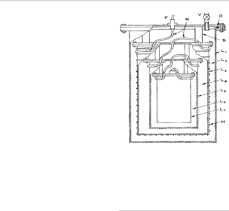
experiments are difficult in stirred baths because bubbles
and debris get into the optical path. For many experiments,
the vibrations that are inevitable in a stirred bath cannot be
tolerated. Much of the work on enclosure thermostats is in
the literature on cryogenics (‘‘cryostats’’)
35,36,39,40
and on
calorimetry.
83–85
In an enclosure thermostat, sometimes called an ‘‘onion’’
thermostat, the temperature is controlled by means of con-
centric layers that are in sequence thermally insulating,
thermally conducting, and thermally controlled.
75,86
The
insulating layers are usually vacuum regions. The conduct-
ing layers are made of metal. A controlled (conducting)
layer has a heater and a thermometer, connected to a con-
troller (see above). The innermost conducting layer is the
experimental stage or block. The result is that the alternat-
ing layers of conductors and insulators attenuate thermal
gradients and fluctuations, making them smaller and smaller
as the central experimental stage is neared. There are two
design concepts for such a thermostat. The first maximizes
the heat capacities of the layers in order to reduce the ther-
mal gradients.
76
The disadvantage of this approach is that
the time constants are very long, and the changes in temper-
ature are very slow. The second design concept maximizes
the number of stages in order to attenuate gradients; this
approach has the advantage of short time constants, but is
limited by practical size considerations.
73
The only commercially available enclosure thermostats
are cryostats for low-temperature regimes,
39
so it is useful
to discuss designs for higher temperatures and for more
general purposes. Figure 8.8 shows a configuration for a
simple
enclosure that will control temperature to 1 mK or
better. There are four conducting layers and three insulat-
ing layers (all vacuum) in this thermostat. This thermostat
can operate only at temperatures above that of its outer-
most layer. Thus that outer layer must be provided with a
means of achieving the required temperature, usually
about 0.5 K below the temperature at the experimental
stage. For temperatures between room temperature and
about 20 K above room temperature, the outer layer can
be left at room temperature. For temperatures below room
temperature, the outer layer can be immersed in a cold bath
or can have copper tubing soldered around it, through
which cold liquid can be circulated. For example, to oper-
ate between 77 and 127 K, the vacuum container could be
immersed in liquid nitrogen. Likewise, for temperatures
more than 20 K above room temperature, a hot bath or
hot circulating liquid can be used.
For some designs, it may be possible to use thermo-
electric coolers (TEC or Peltier devices)
66,77,79
or minia-
ture refrigerators to provide cooling below ambient. Recall
that for a Peltier device, a current through metal junctions
induces a temperature difference. A TEC device has the
advantage that it can be either a heater or a cooler,
Figure 8.8 A simple enclosure thermostat. The thermostat is
made of seven layers. The outer layer (L
1
) is a vacuum
container made of thermally conducting metal and held at a
temperature slightly below the desired set point. The lid is
sealed with the O-ring seal at O, and the can is evacuated by
means of valve V. Layers L
2
,L
4
, and L
6
are insulating vacuum
layers. Layer L
3
is a thermally conducting controlled layer,
wound with heater H and fitted with a control thermometer
(not shown). Layer L
5
is a conducting layer. L
7
is the experimental
stage or block. Supports (S) are made of an insulator such
as nylon. Wires (W) to the thermometers, heaters, and
experimental transducers enter through the feedthrough (F)
and are thermally anchored on each successive stage.
620 MEASUREMENT AND CONTROL OF TEMPERATURE620 MEASUREMENT AND CONTROL OF TEMPERATURE

depending on the direction of the current through it; it has
the disadvantage that in the cooling mode, the heat
removed from the system must be disposed of by some
kind of heat exchanger (flowing air or water). One TEC
can pump up to 125 W, and they can be cascaded for
increased cooling. Devices cost $10 to $100 (Marlow, Mel-
cor, Ferro Tec). The Ferro Tec webpage has an introduc-
tion and design guide. Miniature refrigerators operate on
the principle of Joule–Thomson cooling. They require
flowing gas as the heat exchanger and, depending on the
choice of gas, can operate at temperatures between 83 and
303 K, with a cooling capacity of 0.5 to 10 W/cm
2
per
stage and control of 60.1 K (MMR Technologies, starting
at $1690).
Of course, the choice of solders, insulating materials,
etc., will depend on the temperature range of operation.
Copper is the best choice for conducting layers (see Table
8.5), but aluminum is not bad and is much lighter. Isolation
between
stages can be further increased if radiative losses
are reduced by having conducting stages of low emissivity
(Table 8.5).
While Figure 8.8 shows an evacuated thermostat, it is
often
convenient for the insulating layer to be air. In fact,
the thermal conductivity of air is not significantly
decreased as the pressure decreases until the pressure rea-
ches about 10
4
torr. Thus air at 1 atm is just as good an
insulator as an evacuated space, unless low pressures can
be achieved. At low temperatures, a disadvantage of air is
that water can condense from it, but the air can be dried or
dry nitrogen can be used. A disadvantage of a vacuum is
that vibrations from the vacuum pump are transmitted to
the thermostat.
The heater in Figure 8.8 is a wire, wound symmetrically
and
bifilarly (to reduce inductive effects) on the outside of
the controlled layer. The heater is shown as simply glued to
the outside of the layer, but better thermal contact is
obtained if the wire is glued into grooves machined into
the metal. Manganin wire is good for heaters because it has
a high electrical resistivity that does not change signifi-
cantly with temperature (MWS Wire Industries). Foil heat-
ers that can be glued on where needed are often useful for
the end plates (Omega Engineering, Minco). It is important
that the heater power be distributed as evenly as possible
over the controlled layer. The total heater power must be
calculated from the estimated heat losses for the thermo-
stat. A thermostat like that in Figure 8.8, 18 cm high and 18
cm
in diameter and operating between 273 and 313 K,
requires a heater of 315 X, operated at 0–15 V.
Since the heat distribution is entirely passive, attention
must be given to all unsymmetrical heat losses that could
lead to temperature gradients. All support pieces connecting
one layer to another must be of an insulating material (such
as nylon or glass) and should present a minimum cross-
section for heat transfer. All wires entering the thermostat
should be of the smallest possible diameter. All wires must
be thermally anchored at each stage: they must be wrapped
around the stage in good thermal contact with it, so that they
will come to the temperature of that stage. Since windows in
a thermostat easily cause gradients, they must be kept small
and measures taken to compensate for losses through them.
Cryostats or dewars for low temperatures are often
designed and constructed by scientists,
36,39
but are also
commercially available (Cryomech, Advanced Research
Systems, Janis).
Cited References
1. T. J. Quinn, Temperature, 2nd edn., Academic Press,
New York, 1990.
2. J. F. Schooley, Thermometry, CRC Press, Inc., Boca Raton,
FL, 1986.
3. P. R. N. Childs, J. R. Greenwood, and C. A. Long, Rev. Sci.
Instrum., 71, 2959–2978, 2000.
4. J. Fischer and B. Fellmuth, Rep. Prog. Phys., 68, 1043–
1094, 2005.
5. J. A. Wise, Liquid-in-Glass Thermometry, US Government
Printing Office, Washington, DC, 1976.
6. Handbook of Temperature Measurement: Resistance and
Liquid-in-Glass Thermometry, Vol. 2, R. E. Bentley (Ed.),
Springer, Singapore, 1998.
7. D. D. Pollack, Thermocouples: Theory and Properties,
Chemical Rubber Co., Boca Raton, FL, 1991.
8. T. W. Kerlin, Practical Thermocouple Thermometry,
Instrument Society of America, Research Triangle Park,
NC, 1999.
9. Manual on the Use of Thermocouples in Temperature
Measurement, 4th edn., American Society for Testing
Materials International, West Conshohocken, PA, 1993.
10. Handbook of Temperature Measurement: Theory and
Practice of Thermometric Thermometry, Vol. 3,
R. E. Bentley (Ed.), Springer, Singapore, 1998.
REFERENCES 621

11. D. D. Pollack, Thermoelectricity: Theory, Thermometry,
Tool; ASTM Special Publication 852, American Society for
Testing and Materials, Philadelphia, 1985.
12. T. D. McGee, Principles and Methods of Temperature
Measurement, John Wiley & Sons, Inc., New York, 1988.
13. T. J. Seebeck, Ab. K. Akad. Wiss. Berlin 265, 1822–1823,
1821.
14. J. V. Nicholas and D. R. White, Traceable Temperatures:
An Introduction to Temperature Measurement and
Calibration, 2nd edn., John Wiley & Sons, Inc., New York,
2001.
15. J. C. A. Peltier, Ann. Chim. Phys., 56, 371, 1834.
16. L. Michalski, K. Eckersdorf, J. Kucharski, and J. McGhee,
Temperature Measurement, 2nd edn., John Wiley & Sons,
Inc., New York, 2001.
17. N. P. Moiseeva, Meas. Tech., 47, 915–919, 2004.
18. Low Level Measurements Handbook: Precision DC
Current, Voltage, and Resistance Measurements, 6th edn.,
Keithley Instruments, Cleveland, OH, 2007.
19. H. L. Callendar, Phil. Trans. Royal Soc. London, 178, 161–
230, 1887.
20. J. L. Riddle, G. T. Furukawa, and H. H. Plumb, Platinum
Resistance Thermometry, NBS Monograph 126,US
Government Printing Office, Washington, DC, 1973.
21. H. Preston-Thomas, Metrologia, 27, 3–10 (1990).
22. G. A. Lushchaev, V. A. Karchkov, E. I. Fandeev, and
I. K. Sologyan, Measurement Techn., 24, 475–479,
1981.
23. A. A. Khan, A. R. M. Alamoud, and M. A. Al-Turaigi, Intl.
J. Elec., 67, 931–936, 1989.
24. O. B. Verbeke, J. Spinnewijn, and H. Strauven, Rev. Sci.
Instrum., 58, 654–656, 1987.
25. E. A. Tombasov, Z. P. Chepurnaya, and V. V. Yakunin,
Measurement Techn., 34, 935–938, 1991.
26. T. M. Dauphinee and H. Preston-Thomas, Rev. Sci. Instrum.,
25, 884–886, 1954.
27. O. Bourgeois, E. Andre
´
, C. Macovei, and J. Chaussy, Rev.
Sci. Instrum., 77, 126 108/126 101–126 108/126 103, 2006.
28. J. S. Steinhart and S. R. Hart, Deep-Sea Res., 15, 497–503,
1968.
29. H. J. Hoge, Rev. Sci. Instrum .,
59,
975–979, 1988.
30. T. J. Edwards, Rev. Sci. Instrum., 54, 613–617, 1983.
31. J. Schuderer, T. Schmid, G. Urban, T. Samaras, and
N. Kuster, Phys. Med. Biol., 49, N83–N92, 2004.
32. J. J. Connelly, in Handbook of Temperature Measurement:
Resistance and Liquid-in-Glass Thermometry, Vol. 2, R. E.
Bentley (Ed.), Springer, Singapore, 1998, pp. 55–82.
33. M. J. Pertijs and J. H. Huijsing, Precision Temperature
Sensors in CMOS Technology, Springer, Dordrecht, 2006.
34. J. T. Tuoriniemi and T. A. Knuuttila, Physica B, 280, 474–
478, 2000.
35. A. C. Rose-Innes, Low Temperature Techniques, The
English Universities Press, Inc., London, 1964.
36. R. C. Richardson and E. N. Smith (Eds.), Experimental
Techniques in Condensed Matter Physics at Low
Temperatures, Addison Wesley, Reading, MA, 1998.
37. F. Pobell, Matter and Methods at Low Temperatures, 3rd
edn., Springer, New York, 2007.
38. A. Kent, Experimental Low-Temperature Physics, AIP
Press, New York, 1993.
39. J. Ekin, Experimental Techniques: Cryostat Design,
Material Properties and Superconductor Critical-Current
Testing, Oxford University Press, Oxford, 2006.
40. G. K. White and P. J. Meeson, Experimental Techniques in
Low-Temperature Physics, 4th edn., Clarendon Press,
Oxford, 2002.
41. D. S. Betts, An Introduction to Millikelvin Technology,
Cambridge University Press, Cambridge, 1989.
42. G. Schuster, D. Hechtfischer, and B. Fellmuth, Rept Prog.
Phys., 57, 187–230, 1994.
43. R. Sahul, V. Tasovski, and T. S. Sudarshan, Sens. Actuat. A:
Physical, 125, 358–362, 2006.
44. Y. Hu, in Experimental Techniques in Condensed Matter
Physics at Low Temperatures, R. C. Richardson, R. P. Feyn-
man, and E. N. Smith (Eds.), Westview Press, New York,
1998, pp. 308–320.
45. E. L. Ziercher, K. I. Blum, and Y. Hu, in Experimental
Techniques in Condensed Matter Physics at Low
Temperatures, R. C. Richardson, R. P. Feynman, and E. N.
Smith (Eds.), Westview Publisher, New York, 1998.
46. F. Pavese and G. Molinar, Modern Gas-Based
Temperature and Pressure Measurements,PlenumPress,
New York, 1982.
47. W. Ni, J. S. Xia, E. D. Adams, P. S. Haskins, and
J. E. McKisson, J. Low Temp. Phys., 101, 305–310, 1995.
48. E. Pentii, J. Tuoriniemi, A. Salmela, and A. Sebedash, Rev.
Sci. Instrum., 146, 71–83, 2007.
49. R. J. Soulen, W. E. Fogle, and J. H. Colwell, J
. Low Temp.
Phys., 94, 385–487, 1994.
50. L. Spietz, R. J. Schoelkopf, and P. Pari, Appl. Phys. Lett.,
89, 183123/1–183123/3 (2006).
51. J. P. Kauppinen, K. T. Loberg, A. J. Manninen, and J. P.
Pekola, Rev. Sci. Instrum., 69, 4166–4175, 1998.
52. C. Buchal, J. Hanssen, R. M. Mueller, and F. Pobell, Rev.
Sci. Instrum., 49, 1360–1361, 1978.
53. D. P. DeWitt and G. D. Nutter, Theory and Practice of
Radiation Thermometry, Wiley Interscience, New York,
1988.
622 MEASUREMENT AND CONTROL OF TEMPERATURE

54. M. J. Ballico, in Handbook of Temperature Measurement:
Temperature and Humidity Measurement, Vol. 2, R. E.
Bentley (Eds.), Springer, Singapore, 1998, pp. 67–98.
55. P. Poulsen and S. K. Ault, Rev. Sci. Instrum., 77, 094901/1–
094901/6, 2006.
56. K. T. V. Grattan and Z. Y. Zhang, Fiber Optic Fluorescence
Thermometry, Chapman and Hall, London, 1995.
57. T. Jigami, M. Kobayashi, Y. Taguchi, and Y. Nagasaka, Intl.
J. Thermophys., 28, 968–979, 2007.
58. G. A. Marcus and H. A. Schwettman, J. Phys. Chem. B,
111, 3048–3054, 2007.
59. J. Lee, N. A. Kotov, Nano Today, 2, 48–51, 2007.
60. B. W. Mangum, G. T. Furukawa, K. G. Kreider, et al.
J. Res. Natl. Inst. Stand. Tech., 106, 105–149, 2001.
61. E. B. Wilson, An Introduction to Scientific Research,
McGraw-Hill, New York, 1952.
62. R. E. Rondeau, J. Chem. Eng. Data, 11, 124, 1966.
63. A. M. Phipps and D. N. Hume, J. Chem. Ed., 45, 664, 1968.
64. G. S. Coyne, The Laboratory Companion: A Practical
Guide to Materials, Equipment, and Technique, 2nd edn.,
Wiley-Interscience, New York, 2005.
65. J. Tapping, in Handbook of Temperature Measurement:
Temperature and Humidity Measurement, Vol. 1, R. E.
Bentley (Ed.), Springer, Singapore, 1998, pp. 203–214.
66. A.W. Sloman, P. Buggs, J. Malloy, and D. Stewart, Meas.
Sci. Tech., 7, 1653–1664, 1996.
67. E. D. West, in Treatise in Analytical Chemistry,I.M.
Kolthoff and P. J. Elving (Eds.), John Wiley & Sons, Inc.,
New York, 1967.
68. M. Kutz, Temperature Control, John Wiley & Sons, Inc.,
New York, 1968.
69. M. V. Swaay, J. Chem. Ed. 46, A515–A518, 1969.
70. W. K. Roots, Fundamentals of Temperature Control,
Academic Press, New York, 1969.
71. E. M. Forgan, Cryogenics, 14, 207–214, 1974.
72. J. R. Leigh, Temperature Measurement and Control, Peter
Peregrinus Ltd., London, 1988.
73. D. Sarid and D. S. Cannell, Rev. Sci. Instrum., 45,1082–
1088, 1974.
74. L. Bruschi, R. Storti, and G. Torzo,
Rev. Sci. Instrum., 56,
427–429,
1985.
75. P. K. M. Unni, M. K. Gunasekaran, and A. Kumar, Rev. Sci.
Instrum., 74, 231–242, 2003.
76. B. J. Thysse, J. Chem. Phys., 74, 4678–4692, 1981.
77. X. Zhu, E. Krochmann, and J. Chen, Rev. Sci. Instrum., 63,
1999–2003, 1992.
78. R. B. Strem, B. K. Das, and S. C. Greer, Rev. Sci. Instrum.,
52, 1705–1708, 1981.
79. A. Kojima, C. Ishii, K. Tozaki, et al. Rev. Sci. Instrum., 68,
2301–2304, 1997.
80. P. Cofrancesco, U. Ruffina, M. Villa, P. Grossi, and
R. Scattolini, Rev. Sci. Instrum., 62, 1311–1316, 1991.
81. H. Ogasawara, Rev. Sci. Instrum., 57, 3048–3052, 1986.
82. E. C. Harrigan, Calibration enclosures, in Handbook of
Temperature Measurement: Resistance and Liquid-in-Glass
Thermometry, Vol. 2, R. E. Bentley (Ed.), Springer,
Singapore, 1998, pp. 145–160.
83. Experimental Thermodynamics, Vol. 1, J. P. McCullough
and D. W. Scott (eds.), Butterworth’s, London, 1969.
84. D. C. Ginnings, Precision Measurement and Calibration:
Selected NBS Papers on Heat, US Government Printing
Office, Washington, DC, 1970.
85. J. L. Hemmerich, J.-C. Loos, A. Miller, and P. Milverton,
Rev. Sci. Instrum., 67, 3877–3884, 1996.
86. T. M. Sporton, J. Phys. E. Sci. Instrum., 5, 317–321, 1972.
General References
American Society for Testing Materials International, Manual on
the Use of Thermocouples in Temperature Measurement, West
Conshohocken, PA, 1993.
R. E. Bentley, Handbook of Temperature Measurement, Springer-
Verlag, Singapore, 1998.
Peter R. N. Childs, Practical Temperature Measurements,
Butterworth-Heinemann, Oxford, 2001.
Jack W. Ekin, Experimental Techniques for Low-Temperature
Measurements: Cryostat Design, Material Properties, and
Superconductor Critical Current Testing, Oxford University
Press, Oxford, 2006.
Thomas D. McGee, Principles and Methods of Temperature
Measurement, John Wiley & Sons, Inc., New York, 1988.
L. Michalski, K. Eckersdorf, J. Kucharski, and J. McGhee,
Temperature Measurement, 2nd edn., John Wiley & Sons, Inc.,
New York, 2001.
National Institute of Standards and Technology, Gaithersburg,
MD, Thermometry Group Website.
J. V. Nicholas and D. R. White, Traceable Temperatures: An
Introduction to Temperature Measurement and Calibration,
2nd edn., John Wiley & Sons, Inc., New York, 2001.
Frank Pobell, Matter and Methods at Low Temperatures,
Springer, Berlin, 1996.
Daniel D. Pollack, Thermocouples: Theory and Properties, CRC
Press, Boca Raton, FL 1991.
Robert C. Richardson and Eric N. Smith (Eds.), Experimental
Techniques in Condensed Matter Physics at Low
Temperatures, Addison-Wesley, Reading, MA, 1998.
REFERENCES 623

T. J. Quinn, Temperature, 2nd edn., Academic, New York, 1990.
J. F. Schooley (Ed.), Temperature: Its Measurement and Control
in Science and Industry, Vol. 5, American Institute of Physics,
New York, 1982. See also other volumes in this series.
J. F. Schooley, Thermometry, CRC Press, Boca Raton, FL, 1986.
J. F. Swindells (Ed.), Precision Measurement and Calibration,
Selected NBS Papers on Temperature, NBS Special
Publication 300, Vol. 2, US Government Printing Office,
Washington, DC, 1968.
Temperatures.com, a website with information and resources on
thermometry.
J. A. Wise, Liquid-in-Glass Thermometry, NBS Monograph
150, US Government Printing Office, Washington, DC,
1976.
624 MEASUREMENT AND CONTROL OF TEMPERATURE

INDEX
Note: Figures and Tables are indicated by italic page numbers
1/f noise 492, 549
Abbe diagram (glass chart) 169
Abbe V number 168
aberrations, imaging system 169,
191, 161, 503, 561
charged-particle optics 333–336
and exact ray tracing 171
ABS thermoplastic 525
a.c. line
ground connection 501
three-wire system 501, 525
a.c. line cord 526
mounting at chassis end 526
a.c. line receptacles 18, 526
circuit diagram symbol(s) 509
accuracy of temperature
measurement 600
achromat lens 169, 189
achromatic doublets (lenses) 169,
169, 191
acoustic absorber 229
acousto-optic modulators 238, 288
acrylic plastics 24
jointing of 24
in optical components 193, 241
properties 20, 233, 234, 241, 525
thermoforming of 24
in vacuum systems 117
active electronic components 363,
402–421
circuit diagram symbol(s) 509
active filters 381, 431
adhesives 34
in vacuum systems 117
admittance 366
Ahrens polarizer
208, 209
Airy function 301
alexandrite lasers 264
aligned section (in drawing) 43
alkali-ion source 344
alligator clips 529
alloy steels 18, 19, 20
alumina ceramics 24
as electrical insulators 130, 356
properties 20, 24, 356, 615
in vacuum systems 116, 130
aluminum and alloys 22, 356
properties 19, 141, 220, 615
in vacuum systems 117, 139,140
aluminum coatings on mirrors 245
aluminum plate, vibration-isolated
optical table 229
American Standard Pipe Thread 37
specifications 73
American Standard threaded
fasteners 26
specifications 71
Amici prisms 199
amplifiers 421–435
classifications 421, 422
frequency ranges 422
impedances 422
stability 434
types 421
see also instrumentation
amplifiers; isolation amplifiers;
operational amplifiers
analog input circuits 485
analog input signals, data
acquisition 196, 472–474, 485
analog multiplexer 458, 474, 475
analog-to-digital converters (ADCs)
453, 456, 458
applications 457, 472, 473, 103
anamorphic laser beam expanders
198, 278
annealing
glass 88–89,166
metals 14
antireflection coatings, dielectric
coatings as 183–184
aperture lenses (electrostatic lenses)
331–332
aperture stop 163, 164
apertures in optical system 163
aplanatic imaging 162
apochromat lens 169
arc lamps 255–257
argon ion lasers 263, 270, 271
arithmetic units 448, 451
arsenic trisulfide glass 241
properties 233, 234, 237, 242
ASA flange joints 119
ASCII computer code 469
aspheric lenses 191–193
aspheric surface 166
astigmatic mirrors 183
astigmatism 170, 171, 191
625

astronomical telescope 189
asymmetric electrostatic lens 330, 500
audio amplifiers 422, 423
auxiliary view 42
avalanche photodiodes (APDs)
574–577
Geiger mode 577
backing pump (for vacuum system)
105
backstreaming in vacuum pumps
109, 110
baffles, vacuum system 127
Bakelite, properties 20, 615
baking, ultrahigh vacuum system
144–145
ball bearings 60–61
ball-mounting schemes for
electrostatic lenses 358
ball-and-socket joints 79, 80
banana plugs 525, 528, 529
band-pass filters 380
optical system 212, 213
band-reject filters 380
bandwidth, amplifier 422
Barber’s rule 349, 354
barium fluoride 238
properties 233, 234, 239
‘‘barrel’’ distortion 172
barrier strips (connectors) 530, 531
baseline restorer circuit 439
BASIC programs, IEEE-488 system
484
batteries, circuit diagram symbol(s)
509
baud rate 469
Bayard–Alpert ionization pressure
gauge 102
Bayer pattern, in imaging arrays 580
bead blasting 142
beam angle 325, 326
beam expanders 190, 198, 355, 278
beam parameter, Gaussian beam 179
beam waist, Gaussian beam 180
beams
bending of 50–52
vibration of 54–55
beamsplitters 90, 182, 185, 186
compared with pellicles 186
bearing mounts 59
bearings 59–61
lubrication of 59, 61, 63,124
in vacuum systems 124
Belleville spring washers 63,124
bending
beams and shafts 50–52
glass tubing 88, 89
sheet metal 11, 10, 441
bending moment 50
formulae 51
beryllium copper (bronze) 19, 22
springs 63
Bessel filter 381
‘‘best form’’ lens 170, 188
biconcave lens 188
biconvex lens 187, 188
bimorph piezoelectric elements 221,
228
binary devices 447,585
binary number system 447
binding posts 528
bipolar junction transistors (BJTs)
406–410
active loads 419
applications 402
case styles 406, 407
circuit diagram symbol(s) 407, 509
configurations 406
current–voltage characteristics 408
current-source circuits 419
junction capacitances 200, 409, 412
operating conditions 410, 412
properties 411
, 413
separate power supplies for
biasing voltages 409, 410
small-signal model 409, 412
bipolar operation of power supplies
443
bipolar pulse shaping 438, 440
birefringence 205
bits 467
black materials and coatings 296,
297, 356
blackbody pyrometry 611
blackbody sources 252–253
practical designs 254
blaze angle (of diffraction gratings)
202
blind scew holes, pumpout holes for
142
block diagrams 436, 441, 455, 475,
479, 480, 489, 490, 494, 505, 506,
507, 508
use when troubleshooting 534
blocking capacitors 425
‘‘blooming’’ due to antireflection
coatings 184
Bode plots 370
inverting amplifier 422, 423
bolometers 548, 594–595
characteristics 551, 592, 593
as thermometers 611
bolted joints, designs 36
Boolean algebra 448
Boolean expressions
logic units 449, 364
vacuum system interlock circuits
460, 462, 522
bootstrapping technique, for
photoconductive detectors 570
boring bar 2
borosilicate glasses 24, 76, 239
properties 78, 79, 233, 235, 240
tungsten-to-glass seal 90, 117,
132
in vacuum systems 115, 116
see also Pyrex glass
Bourdon gauge 100
boxcar integrator 494
brake bending of sheet metal 11, 10
brass 21
properties 19, 615
in vacuum systems 116
brass brazing alloy 32
brazed joints 36
in tubing 39, 40
in vacuum systems 132,141
brazing 30, 31–33
thermocouples 604
breadboard circuit/model 508, 510
prototype circuit boards 510
Brewster angle 177
Brewster-angle prisms 198
in laser systems 269, 270
Brewster windows, lasers 268, 269,
272
bridges, electrical 445–446
626 INDEX

brightness
in charged-particle optics 324–325
of light 162
brightness theorem 286
Brinell hardness scale 14
various materials (listed) 15, 19
British Standard Pipe Thread Tapered
specifications 38, 73
broach 3, 4
broad-band antireflection (BBAR)
coatings 185
bronzes 19, 22
Buna-N synthetic rubber 24, 118
butterfly valve 121
Butterworth filter 295, 381
bytes 467
cables and wires 524–528
see also coaxial cable
CAD (computer-aided design)
programs 40
CAD/CAM software 40, 8, 517
cadmium telluride 245
Calbick lens 331
calcite (CaCO
3
), properties 233, 235,
237
calcium fluoride 238
CAMAC sytem 476
bus 478
connectors 533
camera lenses 189
Cameralink interface standard 581
cameras see digital cameras
capacitance, frequency response of
detectors influenced by 553
capacitance manometers 100, 103
capacitance thermometers 611
capacitive effects, in electrical signal
lines 503–504
capacitors
circuit diagram symbol(s) 509
codes 387
equivalent circuits 386
capillary (glass) tubing 79
carbide-tipped cutters and tools 6
carbon black coating 356
carbon-filament conductor cable
528
carbon steels 18, 19
card cage mounting for circuit
boards 514
case hardening 15
cast iron 18, 19
casting 10–12
cathode-ray-tube guns 340
CCD imaging arrays 580–581
center drill 3, 6
centering optical mount 226
centroid 50
centroidal moment of inertia 50
centroidal polar moment of inertia
52
ceramic cements 34
ceramics 24–25
brazed joints 33
as electrical insulators 130
in vacuum systems 116, 130
cesium bromide 243
properties 233, 235, 237, 243
cesium chloride, properties 233, 235
cesium iodide 243
properties 233, 234, 237, 243
CF (ConFlat-compatible) sealing
system 120
CGA (Compressed Gas Association)
connections 38, 73
channel electron multipliers (CEMs)
556, 557, 587, 588
characters 467
charge-coupled device see CCD
charge-sensitive amplifiers 421, 422
charge-sensitive preamplifier
Bode plot 438
combined with pulse detector 435,
438
test circuit 436, 438
charged-particle beam energy
analyzers 345–353
charged-particle beam technology,
applications 324
charged-particle detectors 358,
585–591
charged-particle lenses 327–338
compared with optical lenses 327
see also electrostatic lenses
charged-particle optical systems
construction of 355–360
magnetic-field control for 358–360
materials used in construction
356–357
vacuum requirements 355–356
see also electron-beam devices;
ion-beam devices
charged-particle optics, basic
concepts 324–327
charged-particle sources 338–345
chassis layout diagram (electronic
circuit) 508
Chebyshev filter 381
chemically resistant glassware 77
chopping, amplifier 425
chopping wheels, optical
modulation using 287
Christiansen filters 215, 216
chromatic aberrations 168
, 191, 335
circle of least confusion 334
circuit analysis 365–369
computer-aided 381
Laplace-transform method
374–377, 376, 379
operational amplifier 428–432
circuit boards
extender boards used when
troubleshooting 535
mounting of 514
perforated 510, 511
prototype 510
see also printed circuit boards
circuit breakers 501
circuit diagrams 508
symbols used 509
circuit theory 362–365
circularly polarized light 147, 205
clamp, operational amplifier as 429,
432
closed-loop control systems 480, 479
closed-loop gain, operational
amplifier 426
CMOS imaging arrays 580–581
CMOS logic devices 464, 465
conversion circuits 466
power MOSFETs switched with
412
CNC (computer numerical control)
machines 8, 9
CO lasers 263, 273
CO
2
lasers, 263, 264, 272–273, 290
INDEX 627

coaxial cable 364, 389, 392
applications 498
procedure for stripping 504
properties 392, 393, 396
coaxial connectors 398–399
assembly procedures 398
circuit diagram symbol(s) 509
types 398
Code V analysis 166
optical table for 167
coherence properties of optical
sources 248
coherent sources 247
see also lasers
coil springs 63
coincidence measurements 436, 498–
500
coincidence time spectrum 498, 499
cold-cathode ionization gauge 103
cold-junction compensation circuits
605
cold traps 126
cold working 14
cold-solder joint 521
collet chuck 5
collision frequency 94
color filters 212
color temperature of lamps 255
coma (aberration) 170, 191
comb filter
electronic 380
optical 212
combinatorial logic units 450
combined pulse detector and
charge-sensitive preamplifier
435, 438
common-mode rejection ratio
(CMRR)
isolation amplifiers 433
operational amplifiers 425,
426, 433, 507
voltmeters 507
comparator circuits, operational
amplifiers as 432
compensation, electronic circuit 380
compensator, in control system 489
complementary metal oxide
semiconductor see CMOS
complex admittance 366
compound lenses 189
compound parabolic concentrators
(CPCs) 195, 115, 196
compound turbomolecular/drag
pumps 108
compression ratio, vacuum pumps
107, 108, 132, 137
computer-aided circuit analysis 381
computer simulations
circuit analysis using 381
electrostatic lenses 338
concave gratings 203
concave meniscus lens 188
concentration ratio, nonimaging
light collector 196
condensers (lenses) 192
conductance of vacuum system 96,
97–98
example calculations 139
confocal Fabry–Perot interferometer
308
conjugate points 162
connectors 528–534
circuit diagram symbol(s) 509
see also coaxial connectors
constant-fraction discriminator 440
constantan 604, 610, 615
constrained motion 57–66
construction considerations
charged-particle optical systems
355–360
electronic equipment 508–533
vacuum systems 131–145
continuous arc lamps 255–257
continuous wave (CW) CO
2
lasers
263, 272, 273
continuous wave (CW) dye lasers 280
tuning range 265
continuous wave (CW) gas lasers
270–273
operating wavelengths 263
continuous wave (CW) lasers, power
outputs 266
continuous wave (CW) solid-state
lasers 275
operating wavelengths 264
continuum sources 247, 252–261
contrast ratio, Fabry–Perot systems
307
control systems 479–481
response parameters 480–481
converging thin lens, paraxial ray
tracing for 160
convex meniscus lens 187, 188
cooling systems, lasers 268
copper 21
oxygen-free high-conductivity 116,
356
properties 19, 615
copper alloys 21
brazing using 32
properties 19
copper mirrors 245
copper vapor lasers 264, 275
copper wire, insulated 524
corner-cube prisms 200–201
corner frequencies, in circuit analysis
369, 370
Coulomb blockade thermometers
611
counter digital-to-analog converter
456, 457
counterbore (tool) 3, 4
counters 453, 455
and power-supply noise 467
crimped connectors, 531, 532, 533
crimping tools 531
critical angle (optical reflection/
refraction) 150, 151
critical backing pressure (vacuum
pumps) 105, 107, 110
critical speed of shaft rotation 55
critically damped amplifiers 378
critically damped resonant circuit,
response 378
crowbar circuits 444
crown glasses 168, 239
cryogenic thermometry 610–611
cryopumps 114
applications 132, 136
cryostats 620–621
cube beamsplitters 185, 186
current noise 549, 550
current sources, bipolar junction
transistors 419
current-voltage relations 364
cutting fluids 4, 7
cuvettes 187
628 INDEX

cyanoacrylate contact adhesives 34
cylindrical electrostatic analyzers 347
cylindrical lenses 195
charged-particle system 329
cylindrical-mirror electrostatic
analyzer 348, 532
cylindrical pressure vessels, design of
53
Czerny–Turner grating
monochromator 296, 298
Czerny–Turner prism
monochromator 295, 296
D-connectors 348, 532, 533
D (delay) flip-flop 453, 454
damping of vibrations 54
dark-noise level, optical detectors
553
data acquisition 467–491
data-acquisition interface 486
data-acquisition systems 458
noise elimination 485
standardized 474–479
see also CAMAC system; NIM
system
data buffer 471
data format 469
data loggers 458, 474
data rates 467, 469
data selector 463, 464
data transmission 469
cables 528
system overhead 470–472
data units 448, 452
date code 535
datum 45
d.c. ground connection 501
d.c.-to-d.c. converters 443
decay time, sample-and-hold circuit
474
decelerating lens, in charged-particle
system 336, 350
decibel (dB) scale 370
decimal number system 447
decoder (data unit) 117, 448, 452
degenerative feedback 434
delay-line applications 395, 498
delay-line shaping 439
Delrin 23, 117, 525
demosaicing 580
demountable glass joints 79–80
demountable pressure fittings 38
demountable vacuum system
connections 118–120
demultiplexer (data unit) 448, 452
depletion-mode transistors 412, 414
output current–voltage
derating 382
desoldering techniques 522
detectivity 550–551
determination of 597
optical detectors, 550, 567, 568,
570, 571, 573, 575
see also spectral detectivity
detector arrays 578–582
detectors
calibration of 597
charged-particle detectors 358,
585–591
classification 548
electronics used with 596
equivalent circuits 435, 583, 590
figures of merit for 550–554
ionizing-radiation detectors 591
optical detectors 547
particle detectors 435, 585
photoconductive detectors
566–572
photoemissive detectors 554–566
photovoltaic detectors 572–578
signal-to-noise ratio calculations
582–585
thermal detectors 591–596
deuterium arc lamp 256
deuterium-filled thyratrons 421
diamond 239
properties 234, 240
diaphragm pressure gauge/sensor
100, 103
in vacuum system interlock circuit
461
diaphragm pumps 106–107
dichroic polarizers 208
dielectric coatings
as antireflection coatings 183, 185
as high-reflectance coatings 185
dielectric-coated mirrors 246
differential-equation method, circuit
analysis using 369–372
differential-pressure flowmeters 104
differential pumping 130, 138–139
applications 138, 257
differential-input amplifiers 425
differentiating circuits 369, 372
charge-sensitive preamplifier 438
operational amplifier 429, 431
diffraction gratings 201–204
see also grating spectrometers
diffractive optics 195
diffusion pumps 109–112
applications 132, 132–135, 356
digital cameras, imaging arrays in
580
digital comparator (arithmetic unit)
448, 451
digital controllers, thermostat 616
digital electronics 447–467
digital multimeter (DMM) 491
digital-to-analog converters (DACs)
453, 456, 455
dimensions, on drawings 44–46
diode lasers 278
operating wavelengths 279
diode-pumped solid-state (DPSS)
lasers 279–280
operating wavelengths 264
diodes 402–406
circuit diagram symbol(s) 509
configurations 402, 405
current–voltage characteristics,
363, 402, 403 , 405
diopters (optical units) 155
direct-coupled amplifiers 425
disc of least confusion 334
disc springs
dispersion
diffraction gratings 203
optical 150
prisms 196
dispersive-type analyzers 346
displacement pumps 106
distortion, imaging system 172
distributed parameters, in high-
frequency electrical connections
364
INDEX 629
characteristics
thermal detectors 592, 593

diverging thin lens, paraxial ray
tracing for 161
doping, semiconductor materials 402
double-beam interferometers
309–314
design considerations 314
see also Mach–Zender
interferometer; Michelson
interferometer; Twyman–Green
interferometer
double Gauss lens 166
modulation transfer function 172,
174
optical table for Code V analysis
167
spot diagrams for 170
double-insulated cases 501
double refraction 151, 205
polarizers using 204, 208, 209
doublets (lenses) 188
dove prisms 199, 200
drafting software 40
drag pumps 107
applications 132, 137
drain wire 528
drawing tools 39
drawings see mechanical drawing(s)
drilled holes
locational accuracy 3
threaded 4
drilling 2–4
glass sheet 91
drills
sizes 68
tool speeds for 4
dual-slope digital-to-analog
converter 456, 457
duoplasmatron ion source 345
duty cycle, signal-enhancement
systems 494, 496
dynamic mass spectrometers 355
dynamic resistance, diodes 405
dynamic systems (logic units) 450
dynamic transfer curve, diode 406
dynode chains (in photomultiplier
tubes) 561–563
dynodes (in photomultiplier tubes)
555, 557
materials used 556–561
Ebert–Fastie monochromator 297
echelle gratings 203
ECL devices 464, 465
conversion circuits 466, 477
efficiency, diffraction gratings 203,
504
einzel (electrostatic) lens 331
elasticity modulus 13
see also Young‘s modulus
elastomers 24
electrical connections, in vacuum
systems 131
electrical discharge machining (EDM)
9
electrical grounds, safety aspects
500–503
electrical insulators, in vacuum
systems 130
electrical signal pickup
capacitive effects 503
inductive effects 504
electrically erasable programmable
ROMs (EEPROMs) 459
electromagnetic interference 505
electromagnetic radiation,
fundamental parameters 147
electromagnetic relays 399
electromagnetic spectrum 147
electron-beam devices
chromatic aberration in 335
construction of 355–360
electron guns 338
design example 340
electron-impact ionization ion
source 343
efficiency 345
electron multipliers 586
coupling via transformer 587, 588
see also channel electron
multipliers (CEMs)
electronic compensation circuits (for
thermocouples) 605
electronic components
active 402–421
circuit diagram symbol(s) 509
passive 382–402
selecting 508
electronic devices, in vacuum systems
131
electronics
amplifiers and pulse electronics
421–441
basic concepts 362–382
construction considerations
508–533
digital electronics 447
grounding 500–507
laws and theorems 364
power supplies 441–446
troubleshooting 534–536
electro-optic modulators
287
electropolishing 142
electrostatic lenses 338
compared with optical lenses
327
computer simulations 338, 342
design example 336
electrodes 357
mounting schemes 358
ellipsoidal mirrors 183
elliptically polarized light 147, 204,
485
embossing of sheet metal 11, 10
emissivity 252
enclosure thermostats 619, 620
encoder (data unit) 448, 452
energy analyzers, charged-particle
beam 345–353
energy-add lens (in electrostatic
energy analyzer) 350–352
energy-level diagram, lasers 267
enhancement-mode transistors 412,
414
output current–voltage
characteristics 415
entrainment pumps 112–115
entrance pupil (in optical system)
162, 163
epoxy adhesives 34
epoxy resins, in vacuum systems 118
equivalent circuits 367, 368
capacitors and resistors 386
detectors 435, 583, 590
field-effect transistor 590
equivalent noise charge (ENC) 591
equivalent noise temperature (in
amplifiers) 493
detectors 583, 590
630 INDEX

erasable programmable ROMs
(EPROMs) 450, 459
erector lens 163
error band (of waveform) 379
etalons 187, 299–302
as filters 212, 284
see also Fabry–Perot etalons
e
´
tendue
Fabry–Perot system 307
optical concentrator 195
eutectic temperature 613, 614
evanescent wave 150
exciplex (excimer) lasers 264, 273
expansion thermometers 601
exponential amplifiers 431
extended source(s), coupling to
aperture 286
extension lines (on drawings) 46
extrinsic photoconductive detectors,
properties 568
extrinsic photoconductivity 566
eyepiece lens 163
F-center lasers 276
f/number
lens 163
monochromator/spectrometer
292
fabrication materials 12–25
fabrication processes 2–12, 25–39
Fabry–Perot etalons 212, 299
properties 303, 304
Fabry–Perot fringes, observation of
305
Fabry–Perot interferometers 299–308
alignment of 229
characteristics 294
compared with other optical
dispersing instruments 295
practical operating configurations
303, 305
spherical-mirror 307
Fabry–Perot semiconductor lasers
279
Fabry–Perot systems
design considerations 308
optical characteristics 303
performance limitations 303
fall time (of pulse) 364
Faraday cup (charged-particle
detector) 358, 585
Faraday materials 211
FAST
TM
logic devices 456,467
ferrofluidic shaft seals 124
ferromagnetic table tops (optical
tables) 229
fiber jumpers (for optical fibers) 219
fiber lasers 264, 275
fiber optic connectors 218
fiber optics 217–219
field curvature (aberration in
imaging system) 172, 191
field lens, electron-optical analog
351
field programmable gate arrays
(FPGAs) 460
field stop 163, 164
field of view (in camera lens) 189
field-effect transistors (FETs) 410–419
applications 402
small-signal equivalent circuit 590
see also junction field-effect
transistor; metal oxide-
semiconductor field-effect
transistors
figures of merit
amplifiers 422
detectors 550–554
sample-and-hold (S/H) circuits 474
filters
electronic 380
optical system 212–217
fine-scale movement in optical
systems 220
finesse, in Fabry–Perot systems, 302,
303, 305
fire-polishing of cut glass tubing 83
first-angle projection 42
fits (between parts) 35, 48
fixed-point cells 605, 612, 613
fixed points (reference
temperatures) 614
fixed resistors 383–384
codes 386
types 383
fixed-voltage power supplies 444
fixed-voltage regulators 444
Fizeau interferometer 308
flash converter (digital-to-analog
converter) 456, 457, 456
flashlamp-pumped dye lasers
270
flashlamps 257–261
detector response determined
using 597
flat mirrors 182
flexures 63–66, 224
flicker noise 492, 549
flint glasses 168, 239, 241
flip-flops 450, 454
float plate glass 315
mirrors 182
floating power supplies 501
flowmeters, in vacuum systems 103
fluid baths (thermostats) 616, 617
materials used 615, 619
fluorescence thermometry 622
fluorocarbon polymers 24, 117
properties 20, 525, 615
see also Teflon
focal lengths 152, 153
focal points 152, 153
foldback current limiting (in power
supplies) 444
force fit(s) 35
forward bias, of diode 402
four-wire measurement techniques,
resistance thermometry 608
Fourier transform spectroscopy 311
framegrabber card (in digital
camera) 581
free spectral range, Fabry–Perot
devices 302, 303
frequency response
detectors 553
operational amplifiers 426
Fresnel criterion 159
Fresnel lenses 193, 194
Fresnel retardation rhombs 211
full adder (arithmetic unit) 448, 451
full-duplex transmission of data 469
fused silica 24, 77, 238
properties 78, 79, 233, 234, 237,
240
see also quartz
fuses 501
circuit diagram symbol(s) 509
fusion splicer (for optical fibers) 218
INDEX 631

GaAlAs lasers 277, 280
gain, amplifier 421
gain margin, amplifier 423, 424
gain profile, laser 267, 268
gain-bandwidth product (GBWP)
422
typical values 426
Galilean telescope 189, 190
gallium arsenide
in optical components 245, 273,
277
properties 233, 235, 244
gas-filled photodetectors 547, 555
gas flow, parameters for specifying
95–96
gas jets, in vacuum systems 127–130
gas kinetic theory 93–95
gas thermometers 610
gaseous ion lasers 270–275
operating wavelengths 263–264
gases
bulk vs molecular behavior 95
molecular velocity 94
residual, in vacuum system 93
gate valves, in vacuum systems 122,
122
gated integrator 494, 495
Gauss lens see double Gauss lens
Gaussian beams 179–182, 278
Gaussian lineshape function 251
Gaussian optics 325
Gaussian waveform 438
Geiger mode avalanche
photodetectors 577
generation–recombination (gr) noise
549, 550
geometrical aberrations 169,
333–335
Gerber file (for printed circuit board
production) 518
germanium
in optical components 244, 273
properties 233,
234, 237, 244
germanium photodiodes 573, 574,
575
getter pumps 113–114
ghost reflections (from mirrors) 182
gimbal mounts 223, 226
Glan–Foucault polarizer 209
Glan–Taylor polarizer 208, 209
glass chart (Abbe diagram) 168, 169
glass fibers 78
glass joints 80
glass laboratory components 78–81
glass rod 78, 79
glass sheet
drilling of 91
sawing of 91–92
glass stopcocks 80–81
glass surfaces, cleaning of 143
glass tubing 78–79
bending 82–83, 88, 89
cutting 82–83, 89
fire-polishing of cut end 83
flaring end 87
grinding end 91
pulling points 83–84
ring seal in 87–88, 89
sealing off 84–85
straight seal in 87, 88
T-seal in 85–87
test-tube end formed in 84–85
glass vacuum accessories 116
glass valves 80, 81
glass-to-metal seals 81, 89–90, 116,
132, 241
glassblower’s tools 81–82
glassblowing skills
81–92
glasses
Abbe diagram (glass chart) 168,
169
chemical composition 76–77
chemical properties 76–77
mechanical properties 78, 233
in optical components 239–241
optical properties 78, 79, 234, 240
thermal properties 77–78, 233, 234
in vacuum systems 115–116
Golay cells 595
characteristics 551, 592, 593
gold coatings on mirrors 247
graded index lenses 193
graded seals 81, 116, 231
granite table tops (optical tables) 229
graphical construction, of image size
and position 159–161, 328
grating spectrometers
characteristics 294, 295
compared with prism
spectrometers 293
graybody emitters 253
grinding 9–10
glass tubing 91
ground loops 506–507
ground-fault interrupters (GFIs)
501
grounds and grounding 507
circuit diagram symbol(s) 509
Gullstrand opthalmoscope 163
Hagen–Poiseuille relation, tube
conductance derived from 97,
104
half adder (arithmetic unit) 448, 451
half-duplex transmission of data
469
half-wave plates 206, 210
hand tools 2
hand-shaking (in data transmission)
470
Ha
¨
nsch-type pulsed dye laser 282
hardness of materials 14
various materials 19, 233
hardness scales 14
hardware, electron-equipment
construction 516
harmonic distortion, amplifiers 424
Hastelloy alloys 21
HC logic devices 467
HCT logic devices 467
heat-and-pull method of removing
components from PCBs 522
heat treatments 14
heliarc welding 34, 117, 141
helical springs 63
helium–cadmium lasers 263, 270,
272
helium melting-curve thermometers
610
helium–neon lasers 263, 268, 272,
299
Helmholtz coils/pairs 359–360
Helmholtz–Lagrange law 325–326
applications 334, 335, 342
hemispherical electrostatic analyzer
349
hexadecimal number system 447
632 INDEX

high-efficiency broad-band
antireflection (HEBBAR)
coatings 185
high-pass circuit 369
analysis of 369–372
Bode plots 370
idealized gain and phase responses
370, 371
Laplace-transform equivalent 377
high-pass filters 380, 429, 431
high pressure, meaning of term 52
high-pressure arc lamps 255–256
high-pressure gas cylinders, CGA
connections 38, 73
high-pressure pulsed discharge
lamps 597
high-pressure systems, windows in
231
high-reflectance coatings, dielectric
coatings as 185
high-temperature thermometry 611
high vacuum
characteristics 94
pumps 109, 132
high-voltage cable 527–528
high-voltage connectors 533, 534
hole-making machines 2–4
holographic gratings 203, 295
holographic nondestructive testing
(HNDT) 17
holographic notch filters 214
hookup wire 526
hoop strain 53
hoop stress 53
hot-carrier-effect photoconductive
detectors 572
hot-cathode ionization pressure
gauges 102, 103
hot-air rework station, removal of
components from PCBs using
522
housekeeping signals (in data
transmission) 470
human eye
cones and rods (receptors) 249
spectral response 249
hybrid pumps 108–109
hydrogen brazing 33
hydrostatic gauges 98–100
ice point (temperature reference)
605, 612–613
ice-point bath 605
, 613
IEEE-488 system 482–483
BASIC program for 484
connectors 482
for measurement of temperature-
dependent dielectric constant of
liquid 482–484
image intensifiers 581
image plane 161, 162
imaging arrays 580–581
imaging spectrographs 299
imaging systems 161, 162–165
impedance
amplifier 422
electric circuit 366–369
optical medium 149, 148
transformation through multilayer
optical systems 177–178
impedances method, use in optics
174–179, 300
incoherent sources 247
Inconel alloys 19, 21
indium antimonide photodiodes 574
indium (gallium) arsenide
photodiodes 573, 574, 575, 577
in imaging arrays 580
signal-to-noise ratio calculations
584
inductive effects, in electrical signal
lines 504
inductors, circuit diagram symbol(s)
509
infrared absorption spectrum,
temperature measurement
using 612
infrared lasers 273, 275, 277
safety precautions 290
infrared polarizers 208
infrared thermometers 611
infrared-transmissive materials
241–245
properties 233, 234–235
input plane (of optical system) 152
instrumentation amplifiers 432
typical specifications 433
insulated gate bipolar transistor
(IGBT) 418
compared with other transistors
418,
419
inductive load switching circuit
418
internal connections 418
insulators, properties 615
integral control, thermostat 616
integrated-circuit (IC) amplifiers
425
integrated-circuit packages
abbreviations 503
code prefixes 151
photodiode + op-amp 574
temperature sensors 609–610,
612
integrated-circuit voltage references
445
integrated-circuits, packages 515
integrating circuit 369
operational amplifier 358, 429,
431
interference filters, characteristics
294
interference fringes, observation of
305–306, 309
interferometers 299–314
additional uses 291
see also Fabry–Perot
interferometer; Mach–Zender
interferometer; Michelson
interferometer; Twyman–Green
interferometer
internal pressure 52–54
internal resistance, of voltage/
current source 365
International Temperature Scale (ITS)
600, 612
triple points used to define 612,
613
intrinsic photoconductive detectors,
properties 567
intrinsic photoconductivity 554,
566
Invar alloy 19, 21
inverting amplifier 422, 429
ion-beam devices, construction of
355–360
ion pumps 115
applications 132, 136, 356
INDEX 633
with titanium sublimation pumps
115, 136
ion sources 343–345
ionization pressure gauges
101–103
vacuum system controllers based
on 135
ionizing radiation, detection of
591
irradiance 249
ISO joints 119, 120
ISO (metric) threads 25, 71
isolation amplifiers 433–434
isolation transformers 503
isolation-mode rejection ratio (IMRR)
433
isolators, electronic 461
isothermal block 605
jig plate 229
J/K flip-flop 450, 454
Johnson noise 491
detectors 549, 583, 584, 590
joining of materials 25–39
joints
demountable glass 79–80
design of 34–37
piping and pressure vessels
37–39
types 35
junction field-effect transistor (JFET)
410
circuit diagram symbol(s) 509
construction (N-channel JFET)
411
current–voltage characteristics
413
Kapton (polyimide) 117, 356, 525,
152–159, 528
Karnaugh maps 448, 450, 462
Kel-F polymer 24, 241
properties 20, 234, 525
Kerr cells 288
KF (Klein flange) vacuum joints 119
kinematic design 57–59
optical mounts 223
Kirchhoff’s laws
365
application 380
Knoopness hardness scale 14, 236
various optical materials (listed)
236
Kovar alloy 21, 81
Kovar-to-glass seals 81, 116,
243
KRS-5 (thallium bromoiodide) 243
properties 236, 237, 243
KRS-6 (thallium chlorobromide)
236, 237
krypton ion lasers 263, 270, 271
laboratory glassblowing skills
81–92
Lambertian radiator 249
blackbody as diffuse radiator
252
radiant intensity characteristics
249
Lambertian source 250
lamp-pumped solid-state laser 270,
271
lamps 254–261
Laplace-transform method
circuit analysis using 374–377,
379
control theory using 479
Laplace transforms 375
control systems 481, 489
pulse electronics 435, 438, 439
large-scale integrated (LSI) circuits
458, 464
MOSFETs used in 412
laser beam
focusability parameter 181
focusing with lens 180–181
laser beam expanders 190, 198, 278
laser diodes 277
laser radiation 283–284
lasers 261–291
detector response time
determined using 597
features of design 268–270
operating wavelengths
263–265
power output(s) 249, 266,
270–272
principles of operation 267–268
safety precautions 290–291
specific systems 270–283
types 266
latch 471
latching relay circuit, in vacuum
system 135
lateral-effect photodetectors (LEPs)
578–580
lathe
component parts 5
cuts made by 5
lathe cutting tools 6
speeds for 4
lathe turning 4–7
lava (aluminium silicate) 25
layout diagram, electronic circuit
508
lead sulfide and lead selenide
photoconductive detectors 570,
570
lead-free solders 31, 521
leak detection, in vacuum systems
143
‘‘leak’’ valves 122
least significant bit (LSB) 447
left-hand circularly polarized light
205
lens aberrations 161, 168, 169,
191
lens aperture (camera lens) 189
lenses and lens systems 187–196
materials 236–245
Lexan (polycarbonate) plastic 20,
24, 525
light collectors, nonimaging 162,
195
light sources 147, 247–261
coupling light to aperture
284–286
safety precautions 289–291
light traps 216
line regulation of power supplies
442
line sources 247, 250–252
line-operated equipment,
floating power supplies used 502
linear circuit theory 363
linear-motion bearings 61
linear polarizers
208
optical isolators using 210
linearizing of response curve 363
634 INDEX

linearly polarized light 147, 204
lineshape functions 251
liquid baths (thermostats),
materials used 615, 617, 618, 619
liquid-in-glass thermometers
601–602, 612
liquid-nitrogen-cooled cryotrap
(for diffusion pump) 111, 126
lithium fluoride 237
properties 10, 237, 238
Littrow monochromator 295
Littrow prisms 197
in laser systems 269,
Littrow-type dye laser 283
load-line analysis, diodes
405–406
load regulation of power supplies
442
lock-in amplifier 495
logarithmic amplifiers 429, 431
logic analyzers 535
logic functions, implementing
464–467
logic gates 447, 449
applications 460–464
sinking capabilities 469
sourcing capabilities 469
logic probe (in troubleshooting)
535
logic pulser (in troubleshooting)
535, 536
logical interlock system, vacuum
system protection by 135
long items, representation on
drawings 44
long-pulse flashlamps 257, 258–
260
long-pulse solid-state lasers 266
long-wavelength-pass filters 214
Lorentzian lineshape function
251
low-pass circuit 369
analysis of 369–372
Bode plots 370
idealized gain and phase responses
69, 370
Laplace-transform equivalent
371
low-pass filters
380, 429, 431
low-temperature thermometry
609–611
low-temperature thermostats 620
lubrication, of bearings 60
Lucite see acrylic plastics
luminance 250
luminosity, optical dispersing
instruments 291, 307
luminous flux 250
lumped circuit components 383
Lyman ghosts 203
Mach–Zender interferometer 313
machinability of material 14
machine screws
materials 27–28
types 26–27
machine-tool operations
electrical discharge machining 9
grinding 9–10
lathe turning 4–7
milling 7–9
surface quality for 10, 12
tolerance for 7, 8, 10, 12
McLeod pressure gauge 99–100,
103
Macor ceramics 20, 25, 116, 356,
615
MacSimion simulation of charged-
particle system 339, 343
Magnaflux stress-detection method
18
magnesia, thermal properties 615
magnesium and alloys 22
magnesium fluoride 238
as coating on aluminum mirrors
245, 246, 247
properties 233, 234, 238
magnesium oxide, properties 234,
237,
242
magnet wire 528
magnetic energy analyzers 353
magnetic-field pickup 504,
magnetic sector mass analyzers 354
magnetic-shielding materials 359,
504
magnetic shields 359–360, 565
magnetic suspension systems 108,
magnetic thermometers 611
magnetoresistance 610
magnification
electrostatic lens 328
optical lens 161
maintenance, vacuum pumps 109,
109
manganin 112, 615
manufacturers’ logos 536
manufacturing date code 535
marginal rays 164, 165
maria (in glass tubing) 87, 89,
245
mass analyzers 354–355
mass spectrometers 103
pressure measurement using 103,
144
mass spectrometry, silicon substrate
487–489, 509
materials 18–25
charged-particle optical system
356–357
joining of 25–39
magnetic-shielding 359
optical system 234–235, 236–247
properties 12–18, 19
vacuum system 115–118
matrix methods for optical analysis
152–159, 528
charged-particle optics 332–333
Maxwell–Boltzmann velocity
distribution law 94
mean free path (between molecular
collisions) 94, 355
mechanical design, physical
principles 49–57
mechanical drawing(s) 39
abbreviations used 46, 47
basic principles 44
dimensions on 44–46
notes 44, 45, 46, 130
symbols used 6, 43, 44
tolerances expressed on 46–48,
49
mechanical pressure gauges 98–100
mechanical properties
brazed joints 32
metals 19
plastics 20
soldered joints 30
INDEX 635

mechanical pumps 105–109
mechanical relays 399
contact-conditioning circuits 401,
402
medium-scale integration (MSI)
464
medium-scale movement in optical
systems 220
melting point
as fixed point temperature 614
various optical materials 233
melting-point baths 613
memories 458–460
memory cell, one-bit 458–459
mercury arc lamp 255
mercury cadmium telluride (MCT)
detectors 570, 574, 578
properties 567, 571, 573, 575
mercury diffusion pumps 111
mercury lamp 251
characteristic lines 252
mercury manometer 98, 99, 103
mercury-in-glass thermometers 601–
602
meridional rays, imaging of 170,
171
metal mirrors 245–246
metal oxide-semiconductor field-
effect transistors (MOSFETs) 411–
418
circuit diagram symbol(s) 509
output current–voltage
characteristics 414
structures 414
as switches 412, 474
metal resistance thermometers 605–
607
metal-to-glass seals 81, 89, 116, 132,
241
metal vacuum chambers 139–141
metal vacuum gaskets 120
metal vacuum valves 121–123
metals 18
machining of 4
metering valves
122
meters, circuit diagram symbol(s)
509
metric threaded fasteners 25, 71
specifications 25, 71
mica sheets 357
Michelson interferometer 248, 309–
311
microbolometers 595
microchannel plate (MCP) 556, 557,
588–589
image intensifiers 581
microstrip line 389, 392
microwave lamps 257
Miller effect 367
Miller transform equivalent circuits
367, 368
milling 7–9
cutting operations 7, 8
dimensional accuracy 8, 59
milling cutters 7
speeds for 4, 8
milling machines, types 4, 8
mirror holders/mounts 222–225
mirrors 182–187
materials for 245–247
substrates for 246
‘‘MISER’’ ring laser design 280
mode-locked lasers 266, 284
modems 470
modulation transfer function 172
double Gauss lens 173, 174
modulo-N counters 453
Mohs hardness scale 14
various materials (listed) 15, 623
molecular beams, in vacuum systems
127
molecular-drag pumps 107
applications 132, 137
molecular-nitrogen lasers 264, 275
molecular-sieve vacuum system traps
125–126
molecular thermometers 598
molybdenum
23, 599
Monel alloys 19, 21
monochromators 291
design 295–299
see also spectrometers
Mooney retardation rhomb 211
most significant bit (MSB) 447
motherboard 514
mounts see optical mounts
multichannel analyzer (MCA) 441,
591
multiconductor cable 528
multilayer dielectric coatings on
mirrors 246
multilayer dielectric interference
filter, characteristics 294
multilayer optical systems,
transformation of impedance
through 177–178
multimode lasers 274, 284
multiple-beam interferometers
299–309
see also Fabry–Perot
interferometers
multiple-contact connectors
458, 532
multiple-input data-acquisition
systems 458, 474, 475, 532
multiple monochromators 298
multiplexer (data unit) 448, 452,
622
multiplying digital-to-analog
converter 456
Mylar
electrical properties 525
PCB drafting sheet 520
nanoscale movement in optical
systems 220
nanoscale piezoelectric drives
220–221
near-infrared photodiodes,
properties 573, 574
near-infrared-transmissive materials
239–241
properties 233, 234
negative electron affinity (NEA)
photocathode materials
558–559, 560
properties 558, 560
negative feedback 434
amplifiers with
378, 381
negative-logic system 447, 469
neodymium lasers 264, 265, 275,
290
netlist, printed circuit board
production 517
neutral-density (ND) filters
216
Newton’s formula 328, 332
636 INDEX

Newton’s law 328
nickel, properties 583, 615
nickel alloys 19, 20–21, 359
NIM system 474–476
connectors 475, 476, 533
ECL and TTL conversion circuits
477
logic level specifications 475
modules available 475
nitrogen lasers 264, 275
NMR thermometers 611
noble-gas discharge 256
noise elimination
in data acquisition 485–487
in detectors 553
noise-equivalent power (NEP), of
detectors 550, 584
noise figure (NF) 492
detectors 553–554, 583
noise margin (in logic devices) 464,
465
typical values 465
noise sources 491, 493, 505–506
optical detectors 548–550
noise temperature
amplifiers 493
detectors 588
noise thermometers 610
nonimaging light collectors 162, 195
nonlinear devices 363
nonlinearity, amplifier 441
Norton’s theorem 365
notch hinge 65–66
nuclear instrumentation module see
NIM system
nuclear-orientation thermometers
611
numerical aperture
optical fiber 218
optical system 162
nut-and-bolt assembly, locking
methods 28
Nylon 20, 23, 117,
525, 615
Nyquist noise 549
O-ring joints 79, 80, 118–120
O-ring seals 231
object plane 22, 161
objective lens 163
octagonal prisms 199, 200
octal number system 447
off-null bridges 445
oil diffusion pumps 109–112, 356
oil manometers 98–99, 103
oil-sealed rotary vane pumps
105–106
oil-free vacuum systems 136–138,
356
on–off control, thermostat 234
open-loop control systems 479
open-loop d.c. gain
operational amplifier 426
typical values 426
operational amplifier(s) 425
circuit analysis 428–432
comparison of 741 and OP7
components 426, 427
design rules 427–428
ideal characteristics 425
parameters 425–427
specialized 428
symbol 426
optic axis 205
optical benches 227–228, 228
optical cells 187
optical components 182–219
cleaning of 232–236
mounting of 230–231
positional and orientational
adjustment of 219, 222–229
systems for 219–222
optical concentrators 195–196
optical deflectors 289
optical design
optical detectors 147,
547–548
factors governing choice of
547–548
noise in 548–550
spectral detectivity 550–551, 551
see also photoconductive ...;
photoemissive ...; photovoltaic
detectors
optical dispersing instruments 291–
314
see also interferometers;
monochromators;
spectrographs; spectrometers
optical fibers 217
connectors 218–219
types 218
optical filters 212–216
optical isolators 211–212
see also optically isolated relay
optical lenses 187–196
compared with charged-particle
lenses 327
optical materials
characteristics 233–235
for diffraction gratings 201, 247
factors governing choice 236
for lenses, prisms and windows
236–245
for mirrors 245–247
optical modulators 287–289
optical mounts
characteristics required 220, 222,
230
constructional details 223
optical multichannel analysers
(OMAs) 299
optical parametric oscillators (OPOs)
266, 283
optical sources 147, 247–262
coherence properties 248
optical system(s)
alignment of 229
characterization and analysis of
150–182
design software 178
schematic diagram(s) 152
optical tables 229
selection criteria 229
optical terminology 147–149
optical windows 187
materials 236–245
suppliers 322–323
in vacuum systems 116
, 231,
232
optical-frequency oscillator, laser as
267
optically isolated relay 461
orthographic projection 41–42
oscillators 434–435
outgassing 98
INDEX 637
wavelengths used 168
precision mechanical movement
software 166

output plane (of optical system)
152
overdamped resonant circuit,
response 379
overshoot (of waveform)
overvoltage protection in power
supplies 444
oxygen-free high-conductivity
(OFHC) copper 116, 356
P-polarized wave (TM wave) 176,
175
paraboloidal mirrors 183
parallel circuits, analysis of 366
parallel dimensions 45
parallel format 469
parallel-plate electrostatic analyzers
346–347
parallel resonant circuit 373
current as function of frequency
373
phase relations between voltage
and current 374
parallel–series formats 469
paraxial optics 325
paraxial-ray analysis 151–162
paraxial ray tracing 159–161
parity bit (in data transmission) 470
parity generator/checker (arithmetic
unit) 448, 451
particle-counting experiment 436,
441
particle detectors 435
see also charged-particle
detectors
parts identification 535
passband, energy analyzer 346
passivated implanted planar silicon
(PIPS) solid-state detector,
equivalent noise charge
calculations 591
passive electronic components 363,
382–402
circuit diagram symbol(s) 509
considerations in choice 382–
383
peak reverse voltage (PRV), diodes
402, 403, 407
peak-to-peak voltage 364
pellicles 186–187
compared with beamsplitters 186
Peltier devices 620
Peltier effect 602
pencil angle 326
penta prisms 199, 200
perforated circuit boards 510
,
511
personal computer (PC) control of
experiments 482–491
dielectric-constant temperature
experiment 482–484
example of sensor and control
electronics 487–489
mass spectrometry of silicon
substrate 487–491
Perspex see acrylic plastics
phase margin, amplifier 423, 424
phase-sensitive detection, signal-to-
noise ratio improved by
287
phase-transition baths 613, 614
phase-transition temperatures 614,
612, 613, 619
phenol–formaldehyde
thermosetting plastics 20, 23,
615
phone plugs 530
phosphor thermometry 612
photocathode materials 556–561
properties 552, 559
photocathodes, types 558
photochemical detectors 548
see also photographic film
photoconductive detectors 548,
566–572
biasing circuit for operating 569,
569
cooling of 568, 569
op-amp circuit dor 569
properties 567, 568
spectral detectivity 551, 568,
570
photodiodes 548, 572–578
equivalent circuit 583
signal-to-noise ratio calculations
583–584
photoelastic method of stress
detection 16
photoemissive detectors 548, 554–
566
photoemissive materials, properties
552
, 559
photoemissive surfaces, quantum
efficiency 551
photoexcitation at p–n junction 572,
573
photographic film 548
photometric quantities 250
correspondence with radiometric
quantities 250
photometry 249–250
photomultiplier tubes (PMTs)
anode signal coupling methods
562
cooling of 564, 565
dynode chains in 563
dynodes in 555–556, 557
focusing electrodes 562
mounting of 563
noise in 564–566
practical operational
considerations 561–566
time-response characteristics 553,
555, 563
photomultipliers 555–556
detectivity 555
signal-to-noise ratio calculations
582
photon counting, signal-to-noise
ratio calculations 585
photon detectors 548
spectral sensitivity 548
see also photochemical ...;
photoconductive ...;
photoemissive ...; photovoltaic
detectors
photon-drag detectors 548, 594
photon energy 149
photon-limited performance of
detectors 553
photon noise 548
photons 147
Phototron lamp 144
photovoltaic detectors 548,
572–578
spectral detectivity 551
pickling of metal surfaces 143
638 INDEX

piecewise linear model, diode I–V
characteristic curve represented
by 405
Pierce diode geometry (in electron
guns) 340, 344
pencil angle characteristic 340,
342
piezoelectric pressure transducer
100, 103
piezoelectric scanning
(wavelength scanning) in
interferometers 305
piezoelectric transducers (PZTs),
positioning of optical
components using 220–222, 228
piezotubes 221
‘‘pincushion’’ distortion 172
pins 29
pipe threads 37, 118
specifications
piping, joints in 37–39
Pirani pressure gauge/sensor 101,
103, 135
piston pumps 106
piston-type/poppet valves 121, 122
pitch, graded index lenses 193
pitch of threads 25
pipe threads 73
screw threads 71
plain bearings 59–60
plane mirrors, optical systems with
158
plano-concave lens 188
plano-convex lens 187, 188
plastic films, optical applications
244
plastics 23–24
far-infrared optical applications
244
in optical components 241
properties 241
in vacuum systems 117–118, 356
platinum, properties 615
platinum resistance thermometers
(PRTs) 606, 612
Plexiglass see acrylic plastics
Pockel’s cells (electro-optic
modulators) 287
point source(s) 248
coupling to aperture
284–286
coupling to optical fiber 286
Poisson distribution 497
Poisson’s ratio 14
polariscope, strain in glass observed
by 89, 90
polarization-maintaining (PM) fiber
219
polarized light 204–206
polarizers 204–211
pole-zero compensation 380, 423,
438
polyamides 20, 23, 525
polycarbonate plastics 24, 117, 525
polygon prisms 199, 200
polyimides
insulated cables 528
properties 20, 525
in vacuum systems 117
polymethylmethacrylate (PMMA) see
acrylic plastics
‘‘pop’’ (blind) rivets 29, 28
population inversion, lasers 267
Porro prisms 198, 199
position-sensing potentiometers
367
position-sensitive electron detectors
588
positive feedback, in amplifiers 422,
434
positive-logic system 447, 469
potassium bromide, properties 233,
237
potassium chloride 242
properties 145, 216, 242
potassium iodide, properties 233,
234, 237
potentiometers 384,
391
power, lens surface 155
power amplifiers 423
power bipoar junction transistors,
compared with other transistors
419
power bipolar junction transistors
406
power diodes 402
configurations 404, 405
properties 404
power-failure safeguards, vacuum
systems 134
power line see a.c. line
power line entry modules 526
power MOSFETs 412
applications 416, 417
compared with other transistors
418, 419, 37
example circuits 417
operational characteristics 418
output current–voltage
characteristics 416
structure 416
power supplies 441–446
biasing voltages for transistors
409, 410, 425
current–voltage characteristics
442
fixed-voltage 444
floating 501–503
regulator circuits 443–445
specifications 442–443
power-line-coupled noise 505–506
power-supply noise, reduction of
467
Poynting vector 149, 205
preamplifiers 423
pulse electronics 435
precision mechanical stages 219
precision rectifier, operational
amplifier as 429, 431
precision of temperature
measurement 600
preretardation, in charged-particle
system 350
pressure, units 93
pressure gauges
operating ranges 103
in vacuum systems 98–103
pressure scanning (wavelength
scanning) in interferometers 305
pressure vessels
design of 53
joints in 37–39, 52
pressure-tight seals 231
principal planes 152, 153, 327
principal points 152, 153
principal rays 152, 153, 163, 164,
165, 328
INDEX 639
polyethylene 23, 525

printed circuit boards (PCBs)
516–523
circuit-board substrates 516
construction considerations
fabrication from hand-drawn
artwork 520
production of 516–518
schematic-capture and board-
layout software 517, 538
soldering components to
518–520
prism beam-expanders 198
prism spectrometers 291
characteristics 294
compared with grating
spectrometers 293–295
prisms 201
materials 236–245
programmable logic arrays (PLAs)
459
programmable power supplies
443–444
programmable ROMs (PROMs) 450,
459
programmers for 459
truth tables implemented using
459, 460
proportional controllers, thermostat
616
proportional gain, thermostat 616
proportional, integral, and
differential (PID) controllers 481,
616
proportional and integral (PI) control
616
protection diodes (for transistors)
416, 417, 535
prototype circuit boards 510
pulling points in glass tubing
82–83
pulse-counting applications 436, 441,
587
pulse detection and processing 435–
441
pulse-height analysis 438
pulse-height analyzer (PHA) 441,
498
pulse timing systems 436, 439
pulsed amplifiers 378
pulsed dye lasers 281–283
pumping arrangements 281
tuning range 265
pulsed gas lasers 270, 275
operating wavelengths 263
pulsed lasers
detector response time
determined using
energy outputs 266
pulsed solid-state lasers 276–277
mode configurations 266
operating wavelengths 264–265
pumpdown time (for vacuum system)
98
punch and die 11, 10
PVC, electrical properties 525
Pyrex glass 76, 239
properties, 78, 79, 233, 234, 240,
615
see also borosilicate glasses
pyroelectric detectors 548,
593–594
characteristics 551 , 592, 593
operating circuits for 594
pyrometers 611
Q-switching in lasers 266, 276
QF (quick flange) vacuum joints 119
quadrant detectors 578, 579
quadrupole mass analyzer 355
quantum cascade lasers 277
quantum efficiency
photoemissive surfaces/materials
551, 558, 559
photon detectors 552, 554
quantum noise 548–549
quarter-wave plate 206, 208
optical isolator using 210
quartz 24, 77
fiber torsion springs 24, 62
helium permeability 116
optical properties 237, 240
in vacuum systems 115–116
quartz crystal oscillators 434
quartz fibers 78
quartz windows in vacuum systems
116
quasi-optics 148
quenching, of metals 14
quick-connect joints 79, 80, 118,
119
quick-connect terminals 531
R/S (reset/set) flip-flop 454
rack-mounted circuit board 515
radial cylindrical electrostatic
analyzer 347–348
fringing-field correction 352
radiant sensitivity, photoemissive
materials 551, 62–63, 552, 559,
560
radio-frequency interference 420,
443, 505
radiometric quantities 248
correspondence with photometric
quantities 250
radiometry, units and definitions
248–249
random-access memories (RAMs)
458
rare-earth glasses 168, 239
‘‘rat nest,’’ printed circuit board
production 517
ray tracing 159
aberrations and 166–171
paraxial-ray analysis implemented
using 159–161
ray transfer matrices 153
charged-particle optics analysis
using 332–333
optical-system analysis using 153–
159
Rayleigh criterion 302
razor-blade-stack light trap 217
reactances, capacitive or inductive
365
read-only memories (ROMs) 448, 452,
459
reamer 3, 4
recovery time of power supplies
442
rectifier, operational amplifier as
429, 431
reed relays 400
reference ground 507
reflectance 176
oblique-incident waves 177
640 INDEX

reflection 150
polarization changes due to 177,
206–208, 207
reflection coefficient of surface
176
refraction
charged-particle beam
of light 150
refractive index 149, 148
glasses 77, 233
various optical materials (listed)
233
refractory metals 22, 356
properties
regenerative feedback, in amplifiers
422, 434
regulator circuits (in power supplies)
443–445
relays 399–402
residual-gas analyzers (RGAs) 103
resistance temperature detectors
(RTDs) 605
resistance thermometers 605
compared with other
thermometers 612
dissipation factor(s) 608
high-temperature use 611
low-temperature use 610
properties 606
stability requirements 610
resistance thermometry
measurement systems for
608–609
operating circuit(s) 614
resistor programming of power
supplies 443
resistors
circuit diagram symbol(s) 509
codes 384, 386
equivalent circuits 380
fixed 383–384
types 383
variable 384
resolution
energy analyzers 346, 348, 350,
350
mass analyzers 354
optical stage 219
resolving power
diffraction gratings 203
Fabry–Perot devices 302, 303
optical dispersing instruments
291
resonant circuits 372–374
transient response 378
responsivity of detectors 551
optical detectors 572, 574
thermal detectors 593
Reststrahlen filters 215
retaining rings 29–30
retardation plates 208
retardation rhombs 211
retarding-potential analyzers 345
reticons 578
retroreflectors 198, 200–201
reverse bias, of diode 402
rheostats (variable resistors) 384
rhomb retards 211
rhomboid prisms 199, 200
ribbon-and-plane transmission line
384, 389
right-angle prisms 198
right-hand circularly polarized light
205
ring laser resonator 280
ring seal in glass tubing 87–88, 89
ringing (resonant circuits) 378
ripple binary counter 453, 455
rise time (of waveform) 363, 364, 371,
378
riveted joints, designs 36
rivets 28–29
RLC circuit(s) 377
Laplace-transform equivalent
376
pole trajectory for 377
Rochon polarizer 209
Rockwell hardness scale 14
various materials (listed) 15
rod mounts for electrostatic lenses
357
Rogowski TEA laser design 273
roll forming (sheet metal) 11, 10,
441
roller bearings 60
roller-slide assemblies 61
root-mean-square (rms) voltage
364
Roots blowers 106
rotary pumps
105–106
rotators for optical components
226
roughing pump (for vacuum
system) 105
Rowland circle, for concave gratings
298
Rowland ghosts 203
RS 232 C serial interface 469, 471
connector for 532–533
RTV (room temperature
vulcanizing) silicone rubber
24, 34
ruby lasers 238, 276
rugate filters 214, 215
S-polarized wave (TE wave) 176,
175
safe operating area (SOA),
semiconductors 383
safety precautions
electrical 289, 500–503
grinders 10
light sources 289–291
machine tools 8–9
sagittal rays, imaging of 170, 171
sample-and-hold (S/H) circuits 458,
473, 474, 485
sampling time, sample-and-hold
circuit 474
sand casting 10–12
sapphire 25
properties 233, 234, 237, 239
satellites, diffraction-grating defects
203
sawing, glass sheet 91–92
scattering, as diffraction-grating
defect 203
schematic circuit diagrams 508
symbols used 407, 420, 426 , 459,
509
use when troubleshooting 534
Schmitt trigger 432, 432
Schottky devices
467
scintillation counters 591
screw thread
standard specifications 25–26,
71
INDEX 641

terminology 25–26
section (in drawing) 43, 44
sector magnet energy analyzer 353
Seebeck effect 602
Seidel aberrations 170–172
semiconductor detectors
frequency dependence of noise in
549, 550
size/time-constant relationship
553
semiconductor lasers
properties 277–279
representative structures 278,
278
semiconductor materials
doping of 402
electronic applications 402
optical applications 244
properties 233–235, 237, 243,
244
semiconductor photocathodes 548
wavelength dependence of
radiant sensitivity 552
semiconductor resistance
thermometers 607
properties 607
semiconductor thermometers 609–
610
low-temperature use 610
Senarmont polarizer 209
sensitivity, control system 480–481
sensors, vacuum system 100–103,
135
serial format 469
series circuits, analysis of 366
series dimensions 45
series resonant circuit 373
current as function of frequency
373
phase relations between voltage
and current 374
setscrews 27
settling time
analog-to-digital converter 472
digital-to-analog converter 453
waveform 379
Seya–Namioka monochromator
298
shafts
bending of 50–52
twisting of 52
vibration of 54–55
whirl and vibration of 55–57
shear modulus 52, 79
various materials 19
shears, sheet-metal 10
sheet-metal processes 10
for electronic-circuit chassis
construction 515
shift registers 450, 455
and power-supply noise 467
shop processes
casting 10–12
drilling 2–4
electrical discharge machining 9
grinding 9–10
lathe turning 4–7
milling 7–9
sheet-metal processes 10
surface quality for 10, 12
tolerance for 7, 8, 10, 12
Shore hardness scale 14
short-circuit current 365
short-pulse high-power flashlamps
258, 260, 262
short-wavelength-pass filters 214
shot noise 492
detectors 548–549, 582, 583, 590
shoulder screws 29
shrink tubing (for connectors) 533
SI metric threads 25, 71
siemen (SI unit) 366, 421
signal averaging 494
signal diodes 403
properties 404
signal injection, circuit fault
diagnosis using 535
signal-enhancing techniques 494
signal-to-noise ratio (SNR) 491–492,
493
detectors 553–554, 582–585
optimizing 492–493
silicon 244
properties 233, 234, 237,
244
silicon-controlled rectifiers (SCRs)
419–420
applications 402, 421, 444
circuit diagram symbol 509
current regulation by 420
silicon-controlled switch (SCS)
420
circuit diagram symbol
silicon photodiodes , 572, 573, 63,
575
silicon substrate, mass spectrometry
487–491
silicone oils
in diffusion pumps 111
in thermostats 619, 617
silicone rubber
insulated cable 527–528
room temperature vulcanizing
24, 34
silver brazing alloys 32, 117
silver bromide, properties 233, 234,
243
silver chloride, properties 233,
234, 237, 243
silver coatings on mirrors 246
simplex transmission of data 469
Simulation Program with
Integrated-Circuit Emphasis
(SPICE) 381
sine condition, imaging system 162,
163
single-mode lasers 284
singlet lenses 187–188
sinusoidally varying voltage
skimmers, vacuum system 130
skin effect (in electrical conductors)
364, 390
slew rate, operational amplifiers
426
sliding-gate valve 121
slow-blow fuse 501
slush baths 613
small-scale integration (SSI) 464
small-signal model
field-effect transistor 590
transistors 409, 614
Snell’s law 150, 151
applications
177, 196, 300
charged-particle analog 325
soda-lime glass 76
thermal properties 78
sodium chloride 241–242
properties 233, 234, 237
642 INDEX

sodium fluoride, properties 233, 234,
237
solder aspiration 522
solder wick/braid 522
soldered joints 31, 36
in vacuum systems 141
soldering 30–31
connectors 531
printed circuit board
components 518–522
thermocouples 604
third hand device used 532
vacuum systems 141
soldering fluxes 30, 521
soldering guns 521
solid-state amplifiers, general
operating principles 424–428
solid-state detectors (SSDs)
589–591
equivalent circuit 590
solid-state lasers 277
operating wavelengths 264–265
solid-state relays 401–402, 462
sorption pumps 112–113
applications 136, 356
space-charge effect 336
spatial coherence 248
spatial filtering 191
specific heat, various materials
615
spectral detectivity (of detectors)
550–551
various detectors 551
spectral width of optical source
248
spectrofluorometers 291
spectrographs 291
see also spectrometers and
spectrographs
spectrometers and spectrographs
291
calibration of 299
design 295–299
spectrophotometers 291
spectroscopy experiment, data
transfer rate 467, 470
spherical aberration 170, 191
spherical-aberration coefficient
334
spherical electrostatic analyzers
348–350
fringing-field correction 352
spherical mirror Fabry–Perot
interferometers 307
spherical mirrors 159, 183
paraxial ray tracing for 160–161
‘‘spike’’ filters, optical 214, 275
spinning of sheet metal 10, 11
spinning-rotor pressure gauges 101,
103
splice protector (for joined optical
fibers) 219
spot diagrams (optical system) 168,
170
spot welding 34, 35
Sprague capacitors 273
spring rate 62
helical springs
springs 62–63, 552
square-wave testing 371–372
stability, optical mount 220
stacked-plate polarizers 208
stainless steels 18, 21, 356
properties 19, 220, 615
in vacuum systems 116–117,
139–140
stall pressure (vacuum pumps) 105,
107, 110
stamp and die 10, 11
standard cubic centimeter 96, 104
standardized data-acquisition
systems 474–479
static resistance, diodes 405
steady-state accuracy, control system
481
steatite 20
steel(s) 18, 20
properties 19, 141
steel bolts, SAE grades 27
steel vacuum fittings 117
Stefan–Boltzmann law 253
Steinhart–Hart equation 607
step-index optical fiber 218
stigmatic imaging 162
stirred-liquid thermostats 617–619
stopcocks 80–81, 121
straight seal in glass tubing 87, 88
strain 13, 53
stranded line cord 526
tinning of wire 526
stray capacitances, in amplifiers
434
Strehl ratio 173
stress 13
cylinder under internal pressure
53
stress concentration
detection methods 16–18, 89, 90
effect in materials 16–17
stress–strain curves 13
strip line 392
strontium fluoride, properties 233,
13
strontium titanate (SrTiO
3
),
properties 233, 234, 237
styrofoam, thermal properties 615
subtractor circuit (operational
amplifier) 429
successive-approximation digital-to-
analog converter 456, 457
summer circuit (operational
amplifier) 428, 429
summing point (in operational
amplifier) 428
super mirrors 182
superachromat lens 169
supersonic jets, in vacuum systems
128
surface collision frequency 95
surface-ionization ion source 344
surface-mount technology (SMT)
components 384
codes 390
soldering to PCBs 519
surface preparation, for vacuum
systems 142–143, 356
swing valve 121
switches
circuit diagram symbol(s) 614
electrically actuated 402, 409,
474
sync bit (in data transmission) 470
T-seal in glass tubing 85–87
T (toggle) flip-flop 454
tantalum
in capacitors 384, 385
INDEX 643

properties 20
taps and dies 3, 4
drill sizes for 68, 509
Teflon 24
in glass stopcocks and valves 80, 81,
121
insulated cable 528
properties 20, 525, 615
Teflon thread tape 118
telecentric lenses 189
telescopes 189–190
tellurium 233, 235, 245
temperature
control of 600–621
measurement of 600
temperature-control system 487–
489, 490
temperature ranges 536
tempering of metals 14
temporal coherence 248
tensile strength 13
glasses 78
various materials 19
terminology
optical 147–149
screw thread 25–26
terrestrial telescope 189
Tesla coil (for vacuum leak detection)
144
test prod 536
test-prod wire 527
test-tube end, forming in glass tube
84–85
thallium bromide, properties 233,
234
thallium bromoiodide see KRS-5
thallium chlorobromide see KRS-6
thermal capacitance 614
see also specific heat
thermal circuit 614
thermal conductivity
aluminum compared with steel
220
glass 78
various materials 615
thermal-conductivity pressure
gauges 100–101
thermal conductors, properties 615
thermal detectors 591–596
detectivity 550, 551
types 548, 592
see also bolometers; Golay cell;
pyroelectric detectors;
thermopiles
thermal e.m.f. 602
thermal energy 149
thermal expansion coefficient
various materials 19, 220
various optical materials 235
thermal insulators, properties 615
thermal mass flowmeters 104
thermal noise 549, 550
thermal resistance 102
thermal time constant 614
thermionic electron guns 338
thermionic emission, noise due to
564
thermionic ionization pressure
gauges 102, 103
thermistor-based thermometers 607,
612
thermistor bolometers 595
characteristics 551 , 592
operating circuits for 595
thermocouple pressure gauges 101,
103
vacuum system controllers based
on 135
thermocouples 602–605
advantages and disadvantages as
thermometers 605, 612
calibration of 605
construction details 604
high-temperature use 611
low-temperature use 610
principles governing 603
properties 604
reference junction for 605
types 603–604
thermoelectric coolers (TECs) 620–
621
thermometers
calibration of 601–602, 605,
612–613
expansion thermometers 601
resistance thermometers 605
semiconductor thermometers
609–610
very-low-temperature 610–611
thermopiles 548, 593, 603
characteristics 551 , 592, 593
thermoplastics, properties 20, 525
thermostat 378
thermostats 614–621
design considerations 170
materials used 615
thermowells 604
Thevenin’s theorem 365
thick lens
charged-particle lens as 327
geometrical optics 327–328
ray diagrams 156, 188
ray transfer matrix analysis
155–157
thick-film circuits and components
520
‘‘thimble’’ traps 126
thin lens
charged-particle analog 331
ray transfer matrix analysis 157
third-angle projection 41
threaded circular (military-style)
connectors 533, 534
threaded fasteners 25–28
stress concentration in 16
see also machine screws; screw
thread; steel bolts
three-cylinder electrostatic lens 330,
342
three-legged table, constrainted
motion 57, 59
three-terminal circuit(s)
Miller transformations for 367,
368
Y–D transformation for 367,
368
three-terminal devices
fixed-voltage regulators 444
silicon-controlled rectifiers 419–
420
transistors 406,
410
thrust bearings 59–60, 59, 60
thyratron 421
circuit diagram symbol
thyristor
644 INDEX
comparison of 607
thermoelectric effects 487

circuit diagram symbol
See also silicon-controlled
rectifier
tilt adjusters 223
time constant for detectors 553
determination of 597
optical detectors 567, 568,
573
thermal detectors 593
time-correlation techniques 436, 439,
496–500
time-of-flight energy analyzers 345
time-of-flight mass spectrometer
355
time-to-amplitude converter (TAC)
441, 498
time-to-digital converter (TDC)
498
tin-based lead-free solders 31, 521
tin–lead solders 30, 142, 520
tip plugs 528
Ti:sapphire lasers , 264, 265, 275
titanium and alloys 23
titanium dioxide (TiO
2
), properties
233, 234, 237
titanium sublimation pump 113–114
applications 132, 136
with ion pump 115
tolerances
decimal system for specification
47, 48
on drawings 46–48, 49
machine-tool operations 7, 8, 10,
12
relation to production cost 46, 47
tools
electronic-circuit construction
515
glassblowing 81–82
hand 2
sheet metal working 10
torch brazing 32–33
total internal reflection 150–151
transconductance amplifiers 422,
589
transfer functions 374
control systems 480, 482
high-pass circuit 376
low-pass circuit 376
pole-zero compensation network
380
pulse electronics 438, 439
transformer circuit 233
Laplace-transform equivalent
476
transformers 379
circuit diagram symbol(s)
transient response of power supplies
442
transistor-amplifiers, general
operating principles 424–428
transistor isolators 461
transistor switches 409
transistor–transistor logic see TTL
devices
transistors 406–419
circuit diagram symbol(s)
current–voltage characteristics
407
logic device interface circuits 466
operating conditions 410, 412
properties 240,
413
protection diodes used, 416, 417,
535
separate power supplies for
biasing voltages 409, 241,
425
see also bipolar junction
transistors; field-effect
transistors; unijunction
transistors
transit time, photomultiplier tubes
556
transit-time spread, photomultiplier
tubes 555
translation stages 225
with flexure mounts 226, 227
groove mounting arrangements
for 226, 226
transmission coefficient, of optical
transmission curves, optical materials
79, 238–244
transmission lines 389, 389–396
configurations 392
properties 392. see coaxial cable
transmittance, optical media 175
transresistance amplifiers 422
transversely excited atmospheric-
pressure (TEA) CO
2
lasers 273
traps, vacuum system 124–127,
132
triacs 420
applications 402
circuit diagram symbol 509
triangular prisms 198
triboelectric induction 487
trihedral locating holes 223
triple-point measurements 612,
613
trochoidal analyzer 353
troubleshooting, electronics 534–536
truth tables
arithmetic units 451
data units 452
elementary logic gates 449,
364
flip-flops 454
implementation by PROMs 459,
460
Karnaugh maps for 450, 462
vacuum system interlock circuits
461, 462, 463 , 522
TTL devices 464, 465
conversion circuits 466, 477
edge-triggered 467, 468
level-triggered 467
logic probe and pulser 536
open-collector output 467
power MOSFETs switched with
486
in signal-conditioning circuits
467, 468
three-state output 467
tunable diode lasers 277
tungsten 19, 23
tungsten-filament lamps 254–255
tungsten–halogen lamps 254–255
tungsten inert gas (TIG) welding 34,
117, 141
tungsten-to-Pyrex-glass seal 90,
132
tuning-fork chopper devices 287
turbomolecular pump 107–109
applications 137–138, 356, 460
INDEX 645
media boundary
trimmers (variable resistors) 384

combined with molecular drag
pump 108–109, 137
TV tube electron guns 340
twist drills 3
twisted-pair cables 391, 392, 485,
504, 528
twisting, shaft 52
two-axis rotators (for optical
components) 223–225
two-cylinder electrostatic lens
329–330
two-wire transmission line 389,
391
Twyman–Green interferometer 251,
311
ultrahigh pressure equipment 52
ultrahigh vacuum
characteristics 94
pumps 113, 114, 132
sealing materials 120
valves 122
ultrahigh vacuum system(s)
baking of 144–145
oil-free 136–138
small inexpensive 135–136
ultrasonic cleaning
of metal surfaces 143
of optical components 235
ultraviolet detectors 566
ultraviolet lasers 266, 270, 272,
274
safety precautions 291
ultraviolet radiation, safety
precautions 290
ultraviolet-transmissive materials
237–239
properties 233, 234
underdamped resonant circuit
output waveform 378
response 378
unfolding technique, optical systems
with plane mirrors analyzed
using 158
uniaxial crystals 205
unijunction transistors (UJTs)
420–421
applications 420, 421
circuit diagram symbol 509
current–voltage characteristics 421
structure 420
unipotential electrostatic lens 331
universal asynchronous receiver-
transmitters (UARTs) 469
V-coating (antireflection coating)
184
vacuum photodiodes 554
vacuum pumps 104–115
costs 132
operating ranges 105, 106, 107,
109, 113, 114, 115
vacuum system(s)
analytical representation 96
applications 93
conductance formulae 97–98
costs 124–127, 132
demountable connections in
118–120
design and construction 131–145
electronics and electrictricity in
130–131, 132–138
fail-safe mechanisms 120–123,
134
flow measurement in 95,
103–104
hardware 97, 115–131
interlock systems for 135, 139,
460–463
leak detection in 143
master equation for 96,
547
materials used 115–118
mechanical motion in 123–124,
555
molecular beam and gas jets
introduced into 127
molecular-flow regime 95, 298, 97,
127
network equations 96
pressure measurement in
98–103
pumpdown time for 98
residual gases in 93
transition region 97–98
traps and baffles in 124–127, 132
typical systems 130–131, 132–138
valves in 120–123, 134
viscous-flow regime 95, 103–104,
97, 115–131, 139, 460–463
windows in
116, 231, 232
vacuum-tube photodetectors 96,
547, 123–124, 555
vacuum valves 120–123,134
vacuum-ultraviolet detectors 566
vacuum-ultraviolet monochromators
95, 298
valves
glassware 80, 81
vacuum system 120–123, 134
vapor-degreasing procedure, for
optical components 236
vapor diffusion pumps 109–112
vapor-pressure thermometers 610
variable resistors 384
materials 444
types 384, 390
see also potentiometers
variable-voltage regulators 444
velocity of light 148
Venturi pumps 136, 137
‘‘Verdi’’ laser 280
very-high-temperature thermometry
611
very-large-scale integrated (VLSI)
circuits 458, 464
MOSFETs used in 412
very-low-temperature thermometry
610–611
Vespel (polyimide) 20, 117, 525
VHDL programming language (for
FPGAs) 459
vibration, beams and shafts 54–55
vibration isolation of optical system
229
Vickers hardness scale 15
various materials (listed) 15
vignetting 165
charged-particle beam 326
virtual ground 431
virtual images 160
virtual leaks (in vacuum systems)
132
viscous-drag pressure gauges 101
visible- and near-infrared-
transmissive materials 239–241
properties 216, 233
646 INDEX

visual checks (when
troubleshooting) 534
Viton-A elastomer 24, 118, 122
voice coil actuators 228
Voigt lineshape profile 251
voltage-controlled resistor,
transistor as 411
voltage dividers 366–367
Thevenin equivalent 367
voltage programming of power
supplies 443
voltage-to-frequency converters 472,
473
applications 472
Vycor (96% silica) 77, 239
properties 78, 79, 187, 234, 240
water solubility, various optical
materials 234–235
wave–particle duality 147
waveform recovery 495
wavelength scanning in
interferometers 305
wavemeters 299
wedge prisms 199, 200
welded joints 36–37, 36
in vacuum systems 142
welding 33–34
thermocouples 604
Wheatstone bridge 445
white noise 491, 493, 549, 550
‘‘white-light interferometry’’ 309
Wien filters 353, 354
Wien’s displacement law 253
windows see optical windows
‘‘Winston Cone’’ 195
wire nuts 526
wire-and-plane transmission line
389, 392
wire strippers 526,
527
wire terminals 530, 531
Wire Wrap
TM
boards 523–524
advantages 523
wrap list 523, 524
wires and cables 524–528
stripping of 299, 526, 527
see also coaxial cable
wiring, circuit diagram symbol(s)
302
wiring diagrams see schematic
wiring diagrams
Wollaston polarizer 209
wood, properties 20
Wood’s horn (light trap) 216
words 467
work functions, photoemissive
surfaces 554
working drawings, design translated
to 48–49
working-standard thermometers
601–602, 612
working voltages, capacitors 383,
385
X-ray detectors 591
xenon arc lamp 256
xenon flashlamps, 258, 260,
261
Y–D transformation 367, 368
yield strength 13
various materials 19, 52
Young’s modulus 13
glasses 78
various materials 78–81, 141
Zener diodes 402
zero crossing switching 420
zero potential 500
Zerodur glass ceramic 25
zinc selenide
in optical components 243, 272
properties 305, 323, 243
zinc sulfide, properties 305, 323,
242
INDEX 647
